


Memories
I/O Memory
Program and Data
Addressing Modes
1006F–AVR–06/07
ATtiny11/12
The I/O space definition of the ATtiny11/12 is shown in the following table:
Table 5. ATtiny11/12 I/O Space
Address Hex |
Name |
Device |
Function |
|
|
|
|
$3F |
SREG |
ATtiny11/12 |
Status Register |
|
|
|
|
$3B |
GIMSK |
ATtiny11/12 |
General Interrupt Mask Register |
|
|
|
|
$3A |
GIFR |
ATtiny11/12 |
General Interrupt Flag Register |
|
|
|
|
$39 |
TIMSK |
ATtiny11/12 |
Timer/Counter Interrupt Mask Register |
|
|
|
|
$38 |
TIFR |
ATtiny11/12 |
Timer/Counter Interrupt Flag Register |
|
|
|
|
$35 |
MCUCR |
ATtiny11/12 |
MCU Control Register |
|
|
|
|
$34 |
MCUSR |
ATtiny11/12 |
MCU Status Register |
|
|
|
|
$33 |
TCCR0 |
ATtiny11/12 |
Timer/Counter0 Control Register |
|
|
|
|
$32 |
TCNT0 |
ATtiny11/12 |
Timer/Counter0 (8-bit) |
|
|
|
|
$31 |
OSCCAL |
ATtiny12 |
Oscillator Calibration Register |
|
|
|
|
$21 |
WDTCR |
ATtiny11/12 |
Watchdog Timer Control Register |
|
|
|
|
$1E |
EEAR |
ATtiny12 |
EEPROM Address Register |
|
|
|
|
$1D |
EEDR |
ATtiny12 |
EEPROM Data Register |
|
|
|
|
$1C |
EECR |
ATtiny12 |
EEPROM Control Register |
|
|
|
|
$18 |
PORTB |
ATtiny11/12 |
Data Register, Port B |
|
|
|
|
$17 |
DDRB |
ATtiny11/12 |
Data Direction Register, Port B |
|
|
|
|
$16 |
PINB |
ATtiny11/12 |
Input Pins, Port B |
|
|
|
|
$08 |
ACSR |
ATtiny11/12 |
Analog Comparator Control and Status Register |
|
|
|
|
Note: Reserved and unused locations are not shown in the table.
All the different ATtiny11/12 I/O and peripherals are placed in the I/O space. The different I/O locations are accessed by the IN and OUT instructions transferring data between the 32 general-purpose working registers and the I/O space. I/O registers within the address range $00 - $1F are directly bit-accessible using the SBI and CBI instructions. In these registers, the value of single bits can be checked by using the SBIS and SBIC instructions. Refer to the Instruction Set Summary for more details.
For compatibility with future devices, reserved bits should be written to zero if accessed. Reserved I/O memory addressed should never be written.
The different I/O and peripherals control registers are explained in the following sections.
The ATtiny11/12 AVR RISC Microcontroller supports powerful and efficient addressing modes. This section describes the different addressing modes supported in the ATtiny11/12. In the figures, OP means the operation code part of the instruction word. To simplify, not all figures show the exact location of the addressing bits.
13
|
|
|
|
|
|
|
|
|
|
|
|
|
|
|
|
|
|
|
|
|
|
|
|
|
|
|
|
|
|
|
|
|
|
|
|
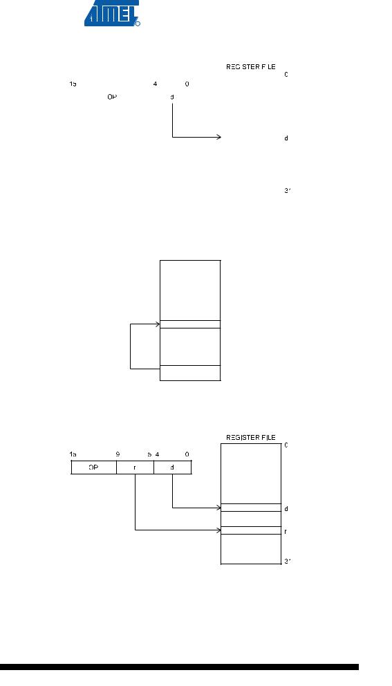
Register Direct, Single |
Figure 8. Direct Single-register Addressing |
||||||||||
Register Rd |
|
|
|
|
|
|
|
|
|
|
|
|
|
|
|
|
|
|
|
|
|
|
|
|
|
|
|
|
|
|
|
|
|
|
|
|
|
|
|
|
|
|
|
|
|
|
|
|
|
|
|
|
|
|
|
|
|
|
|
|
|
|
|
|
|
|
|
|
|
|
|
|
|
|
|
|
|
|
|
|
|
|
|
|
|
|
|
|
|
|
|
|
|
|
|
|
The operand is contained in register d (Rd). |
Register Indirect |
Figure 9. Indirect Register Addressing |
|
REGISTER FILE |
0
Z-register 30
31
The register accessed is the one pointed to by the Z-register (R31, R30).
Register Direct, Two Registers Figure 10. Direct Register Addressing, Two Registers
Rd and Rr
Operands are contained in register r (Rr) and d (Rd). The result is stored in register d (Rd).
14 ATtiny11/12
1006F–AVR–06/07
ATtiny11/12
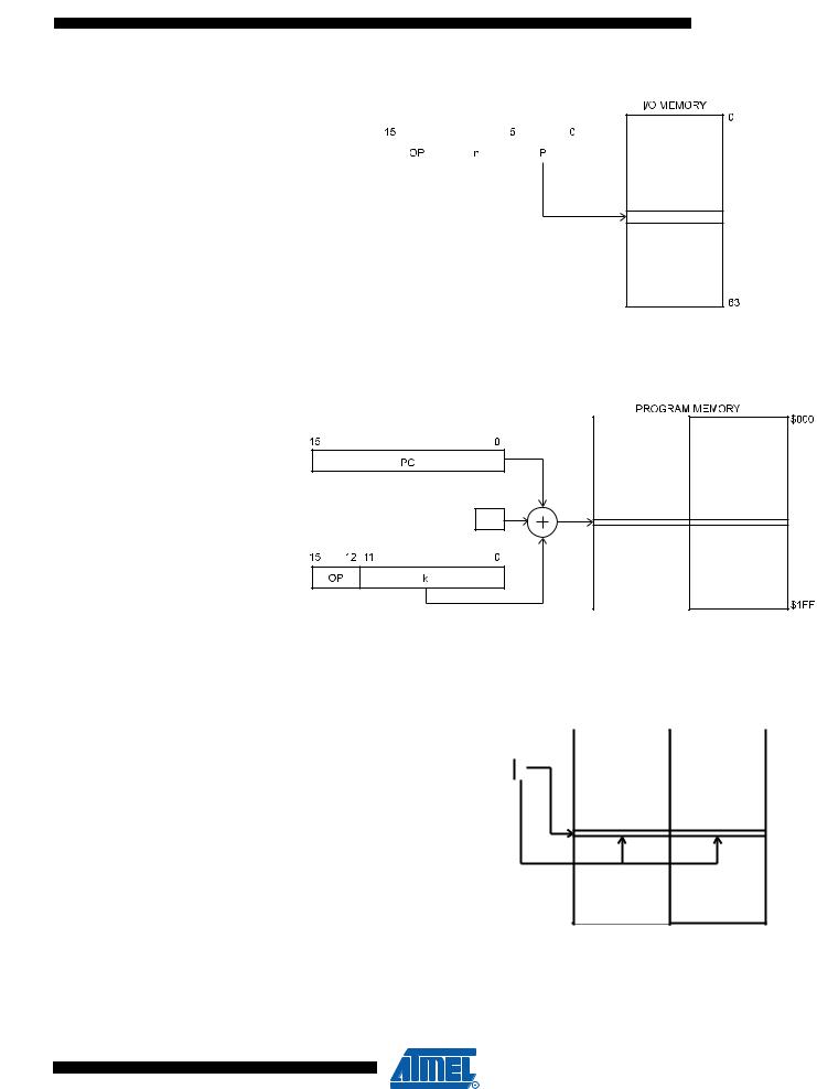
I/O Direct |
Figure 11. I/O Direct Addressing |
|||
|
|
|
|
|
|
|
|
|
|
Operand address is contained in 6 bits of the instruction word. n is the destination or source register address.
Relative Program Addressing, Figure 12. Relative Program Memory Addressing
RJMP and RCALL
+1 |
Program execution continues at address PC + k + 1. The relative address k is -2048 to 2047.
Constant Addressing Using |
Figure 13. Code Memory Constant Addressing |
|||||
the LPM Instruction |
|
|
|
|
|
|
|
|
|
|
|
PROGRAM MEMORY |
|
|
15 |
1 0 |
|
|
$000 |
|
|
|
|
|
|||
|
|
|
Z-REGISTER |
|
|
|
$1FF
Constant byte address is specified by the Z-register contents. The 15 MSBs select word address (0 - 511), the LSB selects low byte if cleared (LSB = 0) or high byte if set (LSB = 1).
15
1006F–AVR–06/07
Memory Access and
Instruction Execution
Timing
This section describes the general access timing concepts for instruction execution and internal memory access.
The AVR CPU is driven by the System Clock Ø, directly generated from the external clock crystal for the chip. No internal clock division is used.
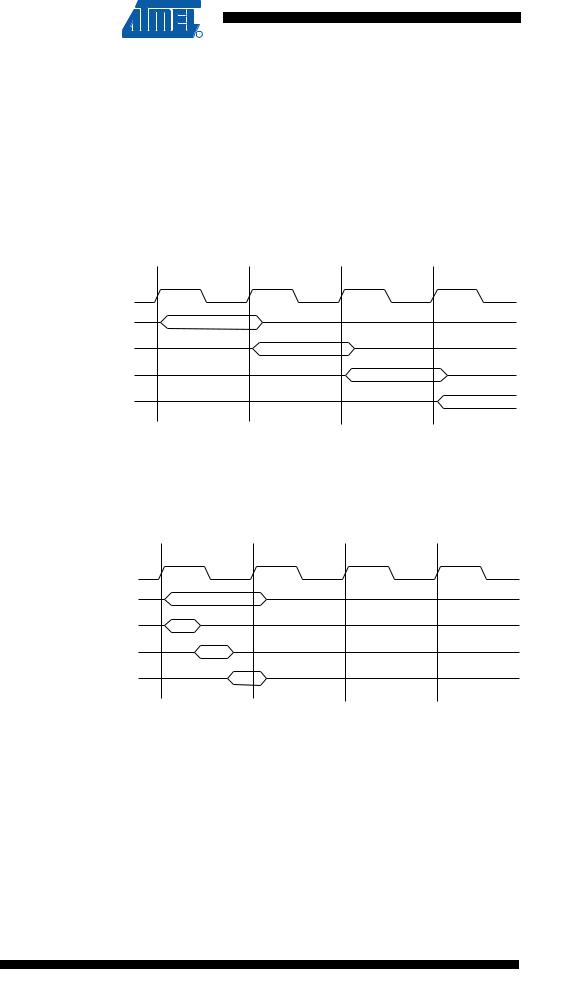
Figure 14 shows the parallel instruction fetches and instruction executions enabled by the Harvard architecture and the fast-access register file concept. This is the basic pipelining concept to obtain up to 1 MIPS per MHz with the corresponding unique results for functions per cost, functions per clocks, and functions per power-unit.
Figure 14. The Parallel Instruction Fetches and Instruction Executions
T1 |
T2 |
T3 |
T4 |
System Clock Ø
1st Instruction Fetch
1st Instruction Execute 2nd Instruction Fetch 2nd Instruction Execute 3rd Instruction Fetch 3rd Instruction Execute 4th Instruction Fetch
Figure shows the internal timing concept for the register file. In a single clock cycle, an ALU operation using two register operands is executed and the result is stored back to the destination register.
Single-cycle ALU Operation
T1 |
T2 |
T3 |
T4 |
System Clock Ø
Total Execution Time
Register Operands Fetch
ALU Operation Execute
Result Write Back
16 ATtiny11/12
1006F–AVR–06/07