


|
|
|
|
ATtiny11/12 |
||
|
|
|
|
|||
|
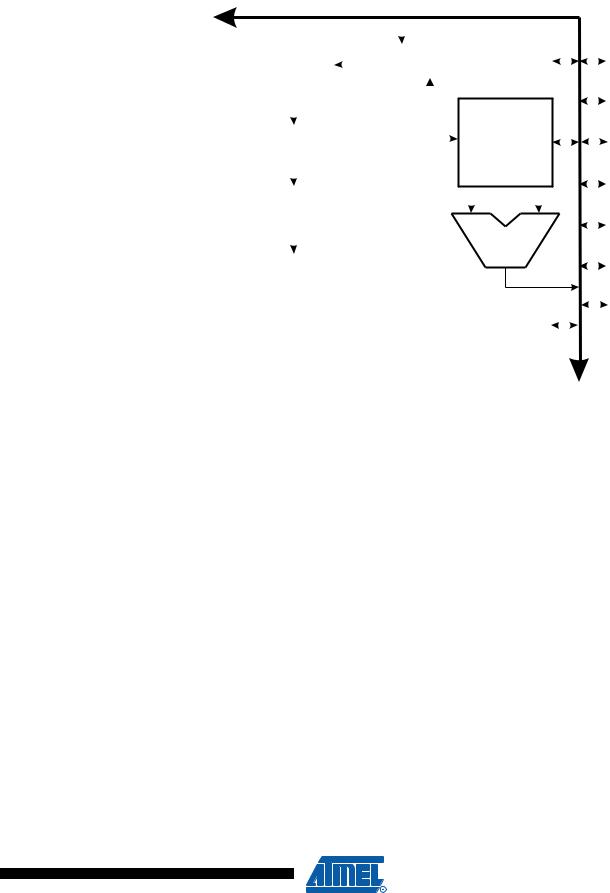
Pin Descriptions |
|
|
|||
|
|
|
|
|
|
|
|
|
|
|
|
|
|
|
VCC |
Supply voltage pin. |
|
|
|
|
|
GND |
Ground pin. |
|
|
|
|
|
Port B (PB5..PB0) |
Port B is a 6-bit I/O port. PB4..0 are I/O pins that can provide internal pull-ups (selected |
||||
|
|
for each bit). On ATtiny11, PB5 is input only. On ATtiny12, PB5 is input or open-drain |
||||
|
|
output. The port pins are tri-stated when a reset condition becomes active, even if the |
||||
|
|
clock is not running. The use of pins PB5..3 as input or I/O pins is limited, depending on |
||||
|
|
reset and clock settings, as shown below. |
|
|
|
|
|
|
Table 2. PB5..PB3 Functionality vs. Device Clocking Options |
|
|
|
|
|
|
|
|
|
|
|
|
|
Device Clocking Option |
PB5 |
|
PB4 |
PB3 |
|
|
|
|
|
|
|
|
|
External Reset Enabled |
Used(1) |
|
-(2) |
- |
|
|
External Reset Disabled |
Input(3)/I/O(4) |
|
- |
- |
|
|
External Crystal |
- |
|
Used |
Used |
|
|
|
|
|
|
|
|
|
External Low-frequency Crystal |
- |
|
Used |
Used |
|
|
|
|
|
|
|
|
|
External Ceramic Resonator |
- |
|
Used |
Used |
|
|
|
|
|
|
|
|
|
External RC Oscillator |
- |
|
I/O(5) |
Used |
|
|
External Clock |
- |
|
I/O |
Used |
|
|
|
|
|
|
|
|
|
Internal RC Oscillator |
- |
|
I/O |
I/O |
|
|
|
|
|
|
|
|
|
Notes: 1. “Used” means the pin is used for reset or clock purposes. |
|
|
|
|
2.“-” means the pin function is unaffected by the option.
3.Input means the pin is a port input pin.
4.On ATtiny11, PB5 is input only. On ATtiny12, PB5 is input or open-drain output.
5.I/O means the pin is a port input/output pin.
XTAL1 |
Input to the inverting oscillator amplifier and input to the internal clock operating circuit. |
|||
XTAL2 |
Output from the inverting oscillator amplifier. |
|||
|
|
Reset input. An external reset is generated by a low level on the |
|
pin. Reset |
RESET |
RESET |
|||
|
|
pulses longer than 50 ns will generate a reset, even if the clock is not running. Shorter |
||
|
|
pulses are not guaranteed to generate a reset. |
||
5
1006F–AVR–06/07

Architectural
Overview
The fast-access register file concept contains 32 x 8-bit general-purpose working registers with a single-clock-cycle access time. This means that during one single clock cycle, one ALU (Arithmetic Logic Unit) operation is executed. Two operands are output from the register file, the operation is executed, and the result is stored back in the register file – in one clock cycle.
Two of the 32 registers can be used as a 16-bit pointer for indirect memory access. This pointer is called the Z-pointer, and can address the register file and the Flash program memory.
The ALU supports arithmetic and logic functions between registers or between a constant and a register. Single-register operations are also executed in the ALU. Figure 2 shows the ATtiny11/12 AVR RISC microcontroller architecture. The AVR uses a Harvard architecture concept with separate memories and buses for program and data memories. The program memory is accessed with a two-stage pipelining. While one instruction is being executed, the next instruction is pre-fetched from the program memory. This concept enables instructions to be executed in every clock cycle. The program memory is reprogrammable Flash memory.
With the relative jump and relative call instructions, the whole 512 address space is directly accessed. All AVR instructions have a single 16-bit word format, meaning that every program memory address contains a single 16-bit instruction.
During interrupts and subroutine calls, the return address program counter (PC) is stored on the stack. The stack is a 3-level-deep hardware stack dedicated for subroutines and interrupts.
The I/O memory space contains 64 addresses for CPU peripheral functions as control registers, timer/counters, and other I/O functions. The memory spaces in the AVR architecture are all linear and regular memory maps.
6 ATtiny11/12
1006F–AVR–06/07
|
|
|
|
|
|
|
|
|
|
|
|
|
|
|
|
|
|
|
|
|
|
ATtiny11/12 |
|||||
|
|
|
|
|
|
|
|
|
|
|
|
|
|
|
|
|
|
|
|
|
|||||||
|
Figure 3. The ATtiny11/12 AVR RISC Architecture |
||||||||||||||||||||||||||
|
|
|
|
|
|
|
|
||||||||||||||||||||
|
|
|
|
|
|
|
|
||||||||||||||||||||
|
|
|
|
|
|
8-bit Data Bus |
|
|
|
|
|
|
|
||||||||||||||
|
|
|
|
|
|
|
|
|
|
|
|
|
|
|
|
|
|
|
|
|
|
|
|
|
|
|
|
|
|
|
|
|
|
|
|
|
|
|
|
|
|
|
|
|
|
|
|
|
|
|
|
|
|
|
|
|
|
|
|
|
|
|
|
|
|
|
|
|
|
|
|
|
|
|
|
|
|
|
|
|
|
|
|
|
|
512 x 16 |
|
|
Program |
|
|
|
Status |
|
|
|
|
|
|
|
|
|
Control |
|
|||||||
|
|
|
|
Counter |
|
|
|
and Test |
|
|
|
|
|
|
|
|
|
Registers |
|
||||||||
|
|
Program |
|
|
|
|
|
|
|
|
|
|
|
|
|
|
|
||||||||||
|
|
|
|
|
|
|
|
|
|
|
|
|
|
|
|
|
|
|
|
|
|
|
|
|
|
||
|
|
Flash |
|
|
|
|
|
|
|
|
|
|
|
|
|
|
|
|
|
|
|
|
|
|
|
|
|
|
|
|
|
|
|
|
|
|
|
|
|
|
|
|
|
|
|
|
|
|
|
|
|
Interrupt |
|
||
|
|
|
|
|
|
|
|
|
|
|
|
|
|
|
|
|
|
|
|
|
|
|
|
|
|
|
|
|
|
|
|
|
|
|
|
|
|
|
|
|
|
32 x 8 |
|
|
|
|
|
Unit |
|
||||||
|
|
|
|
|
|
|
|
|
|
|
|
|
|
|
|
|
|
|
|
|
|||||||
|
|
|
|
|
|
|
|
|
|
|
|
|
|
|
|
|
|
|
|
||||||||
|
|
Instruction |
|
|
|
|
|
|
|
|
|
|
General- |
|
|
|
|
|
SPI Unit |
|
|||||||
|
|
Register |
|
|
|
|
|
|
|
|
|
|
purpose |
|
|
|
|
|
|
|
(ATtiny12 only) |
|
|||||
|
|
|
|
|
|
|
|
|
|
|
|
|
|
Registers |
|
|
|
|
|
|
|
||||||
|
|
|
|
|
|
|
|
|
|
|
|
|
|
|
|
|
|
|
|
|
|||||||
|
|
|
|
|
|
|
|
|
|
|
|
|
|
|
|
|
|
|
|
|
|
|
|
|
|
8-bit |
|
|
|
|
|
Direct Addressing |
|
|
|
|
|
|
|
|
|
|
|||||||||||||
|
|
|
|
|
|
|
|
|
|
|
|
|
|
|
|
|
|
|
Timer/Counter |
|
|||||||
|
|
|
|
|
|
|
|
|
|
|
|
|
|
|
|
|
|
|
|
||||||||
|
|
Instruction |
|
|
|
|
|
|
|
|
|
|
|
|
|
|
|
|
|
|
|
|
|
|
|
||
|
|
|
|
|
|
|
|
|
|
|
|
|
|
|
|
|
|
|
|
|
|
|
|
|
|
||
|
|
Decoder |
|
|
|
|
|
|
|
|
|
|
|
|
|
|
|
|
|
|
|
|
|
|
|
|
|
|
|
|
|
|
|
|
|
|
|
|
|
|
|
|
|
|
|
|
|
|
|
|
|
Watchdog |
|
||
|
|
|
|
|
|
|
|
|
|
|
|
|
|
|
|
|
|
|
|
|
|
|
|
|
|
|
|
|
|
|
|
|
|
|
|
|
|
|
|
|
|
ALU |
|
|
|
|
|
Timer |
|
||||||
|
|
|
|
|
|
|
|
|
|
|
|
|
|
|
|
|
|
|
|
|
|||||||
|
|
|
|
|
|
|
|
|
|
|
|
|
|
|
|
|
|
|
|
||||||||
|
|
Control Lines |
|
|
|
|
|
|
|
|
|
|
|
|
|
|
|
|
|
|
|
|
|
|
Analog |
|
|
|
|
|
|
|
|
|
|
|
|
|
|
|
|
|
|
|
|
|
|
|
|
|
|
Comparator |
|
||
|
|
|
|
|
|
|
|
|
|
|
|
|
|
|
|
|
|
|
|
|
|
|
|
|
|
|
|
|
|
|
|
|
|
|
|
|
|
|
|
|
|
|
|
|
|
|
|
|
|
|
|
|
|
|
|
|
|
|
|
|
|
|
|
|
|
|
|
|
|
|
|
|
|
|
|
|
|
|
|
|
|||
|
|
|
|
|
|
|
|
|
|
|
|
|
|
|
|
|
|
|
|
|
|
|
|
|
|
6 |
|
|
|
|
|
|
|
|
|
|
|
|
|
|
|
|
|
|
|
|
|
|
|
|
|
|
|
I/O Lines |
|
|
|
|
|
|
|
|
|
|
|
|
64 x 8 EEPROM |
|
|
|
|
|
|
|
|
|
|
|
|||||
|
|
|
|
|
|
|
|
|
|
|
|
|
|
|
|
|
|
|
|
|
|||||||
|
|
|
|
|
|
|
|
|
|
|
|
(ATtiny12 only) |
|
|
|
|
|
|
|
|
|
|
|||||
|
|
|
|
|
|
|
|
|
|
|
|
|
|
|
|
|
|
|
|
|
|
|
|
||||
ALU – Arithmetic Logic
Unit
A flexible interrupt module has its control registers in the I/O space with an additional global interrupt enable bit in the status register. All the different interrupts have a separate interrupt vector in the interrupt vector table at the beginning of the program memory. The different interrupts have priority in accordance with their interrupt vector position. The lower the interrupt vector address, the higher the priority.
The high-performance AVR ALU operates in direct connection with all the 32 generalpurpose working registers. Within a single clock cycle, ALU operations between registers in the register file are executed. The ALU operations are divided into three main categories – arithmetic, logic and bit-functions. Some microcontrollers in the AVR product family feature a hardware multiplier in the arithmetic part of the ALU.
Subroutine and Interrupt
Hardware Stack
The ATtiny11/12 uses a 3-level-deep hardware stack for subroutines and interrupts. The hardware stack is 9 bits wide and stores the program counter (PC) return address while subroutines and interrupts are executed.
RCALL instructions and interrupts push the PC return address onto stack level 0, and the data in the other stack levels 1-2 are pushed one level deeper in the stack. When a RET or RETI instruction is executed the returning PC is fetched from stack level 0, and the data in the other stack levels 1-2 are popped one level in the stack.
If more than three subsequent subroutine calls or interrupts are executed, the first values written to the stack are overwritten. Pushing four return addresses A1, A2, A3, and A4, followed by four subroutine or interrupt returns, will pop A4, A3, A2, and once more A2 from the hardware stack.
7
1006F–AVR–06/07

General-purpose
Register File
Figure 4 shows the structure of the 32 general-purpose registers in the CPU.
Figure 4. AVR CPU General-purpose Working Registers
7 |
0 |
|
|
|
R0 |
|
|
|
|
|
R1 |
|
|
|
|
|
R2 |
|
|
|
General- |
|
… |
|
|
|
purpose |
|
… |
|
|
|
Working |
|
R28 |
|
|
|
Registers |
|
R29 |
|
|
|
|
|
R30 (Z-register low byte) |
|
|
|
|
|
R31 (Z-register high byte) |
|
|
|
All the register operating instructions in the instruction set have directand single-cycle access to all registers. The only exception is the five constant arithmetic and logic instructions SBCI, SUBI, CPI, ANDI, and ORI between a constant and a register and the LDI instruction for load-immediate constant data. These instructions apply to the second half of the registers in the register file – R16..R31. The general SBC, SUB, CP, AND, OR and all other operations between two registers or on a single register apply to the entire register file.
Registers 30 and 31 form a 16-bit pointer (the Z-pointer) which is used for indirect Flash memory and register file access. When the register file is accessed, the contents of R31 are discarded by the CPU.
8 ATtiny11/12
1006F–AVR–06/07