


System Control and
Reset
Reset Sources
The ATtiny11/12 provides three or four sources of reset:
•Power-on Reset. The MCU is reset when the supply voltage is below the power-on reset threshold (VPOT).
•External Reset. The MCU is reset when a low level is present on the RESET pin for more than 50 ns.
•Watchdog Reset. The MCU is reset when the Watchdog timer period expires and the Watchdog is enabled.
•Brown-out Reset. The MCU is reset when the supply voltage VCC falls below a certain voltage (ATtiny12 only).
During reset, all I/O registers are then set to their initial values, and the program starts execution from address $000. The instruction placed in address $000 must be an RJMP
– relative jump – instruction to the reset handling routine. If the program never enables an interrupt source, the interrupt vectors are not used, and regular program code can be placed at these locations. The circuit diagram in Figure 15 shows the reset logic for the ATtiny11. Figure 16 shows the reset logic for the ATtiny12. Table 7 defines the electrical parameters of the reset circuitry for ATtiny11. Table 9 shows the parameters of the reset circuitry for ATtiny12.
Figure 15. Reset Logic for the ATtiny11
|
VCC |
|
|
Power-on Reset |
|
POR |
|
|
|
|
|
|
|
|
|
|
|
|
|
|
|
|||
|
|
|
|
|
|
|
|
|
|
|
|
|
|
|
|
|
|
|
|
|
||||
|
|
|
|
|
Circuit |
|
|
|
|
|
|
|
|
|
|
|
|
|
|
|
|
|
INTERNAL RESET |
|
|
|
|
|
|
|
|
|
|
|
|
|
|
|
|
|
|
|
|
|
|
|
|
|
|
|
|
|
|
|
|
|
|
|
|
|
|
|
|
|
|
|
|
|
|
|
|
|
|
|
|
|
|
|
|
Reset Circuit |
|
|
|
|
|
|
RESET |
|
|
|
|
|
|
|
|
||||
|
RESET |
|
|
|
|
|
|
|
|
|
|
|
|
|
S |
Q |
|
|||||||
|
|
|
|
|
|
|
|
|
|
|
|
|
|
|
|
|
|
|||||||
|
|
|
|
|
|
|
|
|
|
|
|
|
COUNTER |
|
|
|
|
|
|
|
|
|
|
|
|
|
|
|
|
|
|
|
|
|
|
|
|
|
|
|
|
|
|
|
|
|
|
|
|
|
|
|
|
|
Watchdog |
|
|
|
|
|
|
|
|
|
|
|
|
|
|
|
|
|
||
|
|
|
|
|
|
|
|
|
|
|
|
|
|
|
|
|
|
|
|
|
|
|
||
|
|
|
|
|
Timer |
|
|
|
|
|
|
|
|
|
|
|
|
|
|
|
|
|
|
|
|
|
|
|
|
|
|
|
|
|
|
|
|
|
|
|
|
|
|
|
|
|
|
|
|
|
|
|
|
|
|
|
|
|
|
|
|
|
|
|
|
|
|
|
|
|
|
|
|
|
|
|
|
|
|
|
|
|
|
|
|
|
|
|
|
|
|
|
|
|
|
|
|
|
|
|
|
|
|
|
|
|
|
|
|
|
|
|
|
|
|
|
|
|
|
|
|
|
|
|
|
|
|
|
|
On-chip |
|
|
|
|
|
|
|
|
|
|
|
|
|
|
|
|
|
|
|
|
|
|
|
|
|
|
20-stage Ripple Counter |
|
|
|
|
|
R |
Q |
|
|
||||||||
|
|
|
|
|
RC Oscillator |
|
|
|
|
|
|
|
|
|
||||||||||
|
|
|
|
|
|
Q3 |
Q9 |
|
|
Q13 |
Q19 |
|
|
|
|
|
|
|
|
|||||
|
|
|
|
|
|
|
|
|
|
|
|
|
|
|
|
|
|
|||||||
|
|
|
|
|
|
|
|
|
|
|
|
|
|
|
|
|
|
|
|
|
|
|
||
|
|
|
|
|
|
|
|
|
|
|
|
|
|
|
|
|
|
|
|
|
|
|
|
|
|
|
|
|
|
|
|
|
|
|
|
|
|
|
|
CKSEL |
FSTRT |
|
|
|
|
||||
Table 7. Reset Characteristics for the ATtiny11
Symbol |
|
Parameter |
Min |
Typ |
Max |
Units |
|
|
|
|
|
|
|
|
|
(1) |
|
Power-on Reset Threshold Voltage (rising) |
1.0 |
1.4 |
1.8 |
V |
|
|
|
|
|
|
|
|
|
VPOT |
|
Power-on Reset Threshold Voltage (falling) |
0.4 |
0.6 |
0.8 |
V |
|
|
|
||||||
|
|
|
|
|
|
|
|
VRST |
|
|
Pin Threshold Voltage |
|
0.6 VCC |
|
V |
RESET |
|
|
|||||
Note: 1. The Power-on Reset will not work unless the supply voltage has been below VPOT (falling).
22 ATtiny11/12
1006F–AVR–06/07

|
|
|
|
|
|
|
|
|
ATtiny11/12 |
|
|
|
|
|
|
|
|
|
|
|
Power-on Reset for the |
|
|
|
|
|
|
|
|
|
A Power-on Reset (POR) circuit ensures that the device is reset from power-on. As |
||||||||
|
|||||||||
|
ATtiny11 |
shown in Figure 15, an internal timer is clocked from the watchdog timer. This timer pre- |
|||||||
|
|
vents the MCU from starting a certain period after VCC has reached the Power-on |
|||||||
|
|
Threshold Voltage – VPOT. See Figure 17. The total reset period is the Delay Time-out |
|||||||
|
|
period – tTOUT. The FSTRT fuse bit in the Flash can be programmed to give a shorter |
|||||||
|
|
start-up time.The start-up times for the different clock options are shown in the following |
|||||||
|
|
table. The Watchdog Oscillator is used for timing the start-up time, and this oscillator is |
|||||||
|
|
voltage dependent as shown in the section “ATtiny11 Typical Characteristics” on page |
|||||||
|
|
62. |
|
|
|
|
|
|
|
|
|
Table 8. Start-up Times for the ATtiny11 (VCC = 2.7V) |
|
|
|||||
|
|
|
|
|
|
Start-up Time tTOUT |
|||
|
|
Selected Clock Option |
FSTRT Unprogrammed |
|
FSTRT Programmed |
||||
|
|
|
|
|
|
|
|||
|
|
External Crystal |
|
67 ms |
|
4.2 ms |
|||
|
|
|
|
|
|
|
|||
|
|
External Ceramic Resonator |
|
67 ms |
|
4.2 ms |
|||
|
|
|
|
|
|
|
|||
|
|
External Low-frequency Crystal |
|
4.2 s |
|
4.2 s |
|||
|
|
|
|
|
|
|
|||
|
|
External RC Oscillator |
|
4.2 ms |
|
67 µs |
|||
|
|
|
|
|
|
|
|||
|
|
Internal RC Oscillator |
|
4.2 ms |
|
67 µs |
|||
|
|
|
|
|
|
|
|
|
|
|
|
External Clock |
|
4.2 ms |
|
5 clocks from reset, |
|||
|
|
|
2 clocks from power-down |
||||||
|
|
|
|
|
|
|
|
||
|
|
|
|
|
|
|
|
||
|
|
If the built-in start-up delay is sufficient, |
|
|
can be connected to VCC directly or via |
||||
|
|
RESET |
|||||||
|
|
an external pull-up resistor. By holding the |
RESET |
pin low for a period after VCC has |
|||||
|
|
been applied, the Power-on Reset period can be extended. Refer to Figure 18 for a tim- |
|||||||
|
|
ing example on this. |
|
|
|
|
|
|
|
23
1006F–AVR–06/07

Figure 16. Reset Logic for the ATtiny12
DATA BUS
Power-on Reset
Circuit
BODEN
Brown-out
BODLEVEL  Reset Circuit
MCU Status
Register (MCUSR)
PORF |
BORF |
EXTRF |
WDRF |
CKSEL[3:0]
|
|
|
|
|
|
|
|
|
|
|
|
|
|
|
|
On-chip |
|
|
Delay Counters |
|
|
||
RC Oscillator |
|
|
Full |
||||
|
|
|
|
||||
|
|
|
|
|
|
||
|
|
|
|
|
|
|
|
|
|
|
|
|
|
|
|
|
|
|
CK |
||||
Table 9. Reset Characteristics for the ATtiny12
Symbol |
|
Parameter |
Condition |
Min |
Typ |
Max |
Units |
|
|
|
|
|
|
|
|
|
|
|
|
Power-on Reset Threshold |
BOD disabled |
1.0 |
1.4 |
1.8 |
V |
|
|
|
|
|
|
|
|
||
(1) |
|
Voltage (rising) |
BOD enabled |
0.6 |
1.2 |
1.8 |
V |
|
|
|
|
||||||
|
|
|
|
|
|
|
|
|
VPOT |
|
Power-on Reset Threshold |
BOD disabled |
0.4 |
0.6 |
0.8 |
V |
|
|
|
|||||||
|
|
|
|
|
|
|
||
|
|
Voltage (falling) |
BOD enabled |
0.6 |
1.2 |
1.8 |
V |
|
|
|
|
|
|||||
|
|
|
|
|
|
|
|
|
|
|
|
Pin Threshold |
|
|
|
|
|
VRST |
|
RESET |
|
|
0.6VCC |
|
V |
|
|
Voltage |
|
|
|
||||
VBOT |
|
Brown-out Reset Threshold |
(BODLEVEL = 1) |
1.5 |
1.8 |
1.9 |
V |
|
|
|
|
|
|
||||
|
Voltage |
(BODLEVEL = 0) |
2.3 |
2.7 |
2.8 |
|||
|
|
|
|
|
||||
|
|
|
|
|
|
|
|
|
Note: 1. The Power-on Reset will not work unless the supply voltage has been below VPOT (falling).
24 ATtiny11/12 
1006F–AVR–06/07

ATtiny11/12
Table 10. ATtiny12 Clock Options and Start-up Times
|
|
Start-up Time, |
Start-up Time, |
|
|
VCC = 1.8V, |
VCC = 2.7V, |
|
|
BODLEVEL |
BODLEVEL |
CKSEL3..0 |
Clock Source |
Unprogrammed |
Programmed |
|
|
|
|
1111 |
Ext. Crystal/Ceramic Resonator(1) |
1K CK |
1K CK |
1110 |
Ext. Crystal/Ceramic Resonator(1) |
3.6 ms + 1K CK |
4.2 ms + 1K CK |
1101 |
Ext. Crystal/Ceramic Resonator(1) |
57 ms 1K CK |
67 ms + 1K CK |
1100 |
Ext. Crystal/Ceramic Resonator |
16K CK |
16K CK |
|
|
|
|
1011 |
Ext. Crystal/Ceramic Resonator |
3.6 ms + 16K CK |
4.2 ms + 16K CK |
|
|
|
|
1010 |
Ext. Crystal/Ceramic Resonator |
57 ms + 16K CK |
67 ms + 16K CK |
|
|
|
|
1001 |
Ext. Low-frequency Crystal |
57 ms + 1K CK |
67 ms + 1K CK |
|
|
|
|
1000 |
Ext. Low-frequency Crystal |
57 ms + 32K CK |
67 ms + 32K CK |
|
|
|
|
0111 |
Ext. RC Oscillator |
6 CK |
6 CK |
|
|
|
|
0110 |
Ext. RC Oscillator |
3.6 ms + 6 CK |
4.2 ms + 6 CK |
|
|
|
|
0101 |
Ext. RC Oscillator |
57 ms + 6 CK |
67 ms + 6 CK |
|
|
|
|
0100 |
Int. RC Oscillator |
6 CK |
6 CK |
|
|
|
|
0011 |
Int. RC Oscillator |
3.6 ms + 6 CK |
4.2 ms + 6 CK |
|
|
|
|
0010 |
Int. RC Oscillator |
57 ms + 6 CK |
67 ms + 6 CK |
|
|
|
|
0001 |
Ext. Clock |
6 CK |
6 CK |
|
|
|
|
0000 |
Ext. Clock |
3.6 ms + 6 CK |
4.2 ms + 6 CK |
|
|
|
|
Note: 1. Due to the limited number of clock cycles in the start-up period, it is recommended that Ceramic Resonator be used.
This table shows the start-up times from reset. From sleep, only the clock counting part of the start-up time is used. The Watchdog oscillator is used for timing the real-time part of the start-up time. The number of WDT oscillator cycles used for each time-out is shown in Table 11.
Table 11. Number of Watchdog Oscillator Cycles
BODLEVEL |
Time-out |
Number of Cycles |
|
|
|
Unprogrammed |
3.6 ms (at Vcc = 1.8V) |
256 |
|
|
|
Unprogrammed |
57 ms (at Vcc = 1.8V) |
4K |
Programmed |
4.2 ms (at Vcc = 2.7V) |
1K |
Programmed |
67 ms (at Vcc = 2.7V) |
16K |
|
|
|
The frequency of the watchdog oscillator is voltage dependent as shown in the section “ATtiny11 Typical Characteristics” on page 62.
Note that the BODLEVEL fuse can be used to select start-up times even if the Brownout Detection is disabled (by leaving the BODEN fuse unprogrammed).
The device is shipped with CKSEL3..0 = 0010.
25
1006F–AVR–06/07
Power-on Reset for the |
|
|
|
|
|
|
|
|
|
|
|
|
|
|
|
|
|
|
|
|
|
|
|
|
|
|
|
|
|
|
|
|
|
|
|
|
|
|
|
|
|
|
|
|
|
|
|
|
|
|
|
|
|
|
|
|
|
|
|
|
|
|
A Power-on Reset (POR) pulse is generated by an on-chip detection circuit. The detec- |
||||||||||||||||||||
ATtiny12 |
tion level is nominally 1.4V. The POR is activated whenever VCC is below the detection |
|||||||||||||||||||
|
level. The POR circuit can be used to trigger the start-up reset, as well as detect a fail- |
|||||||||||||||||||
|
ure in supply voltage. |
|
|
|
|
|
|
|
|
|
|
|
|
|
|
|
||||
|
The Power-on Reset (POR) circuit ensures that the device is reset from power-on. |
|||||||||||||||||||
|
Reaching the Power-on Reset threshold voltage invokes a delay counter, which deter- |
|||||||||||||||||||
|
mines the delay for which the device is kept in Reset after VCC rise. The time-out period |
|||||||||||||||||||
|
of the delay counter can be defined by the user through the CKSEL fuses. The different |
|||||||||||||||||||
|
selections for the delay period are presented in Table 10. The Reset signal is activated |
|||||||||||||||||||
|
again, without any delay, when the VCC decreases below detection level. |
|||||||||||||||||||
|
If the built-in start-up delay is sufficient, |
|
can be connected to VCC directly or via |
|||||||||||||||||
|
RESET |
|||||||||||||||||||
|
an external pull-up resistor. See Figure 17. By holding the |
RESET |
pin low for a period |
|||||||||||||||||
|
after VCC has been applied, the Power-on Reset period can be extended. Refer to Fig- |
|||||||||||||||||||
|
ure 18 for a timing example on this. |
|||||||||||||||||||
|
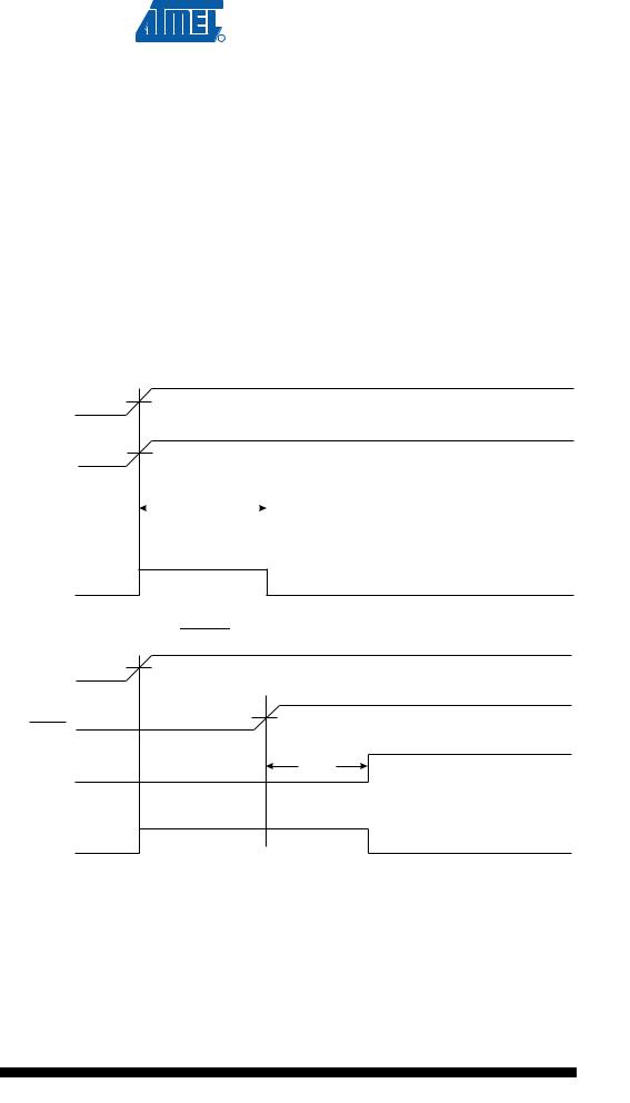
Figure 17. MCU Start-up, |
|
|
|
Tied to VCC. |
|||||||||||||||
|
RESET |
|||||||||||||||||||
|
|
VCC |
VPOT |
|||||||||||||||||
|
|
|
|
|
|
|
|
|
|
|
|
|
|
|
|
|
||||
|
|
|
|
|
|
VRST |
||||||||||||||
|
|
RESET |
||||||||||||||||||
|
|
|
|
|
|
|
|
|
|
|
|
|
|
|
|
|
||||
|
TIME-OUT |
|
|
|
|
|
tTOUT |
|
|
|
|
|||||||||
|
|
|
|
|
|
|
|
|
||||||||||||
|
|
|
|
|
|
|
|
|
|
|
|
|||||||||
INTERNAL
RESET
Figure 18. MCU Start-up, RESET Extended Externally
VPOT
VCC
VRST
RESET
tTOUT
TIME-OUT
INTERNAL
RESET
26 ATtiny11/12
1006F–AVR–06/07