

ATtiny11/12
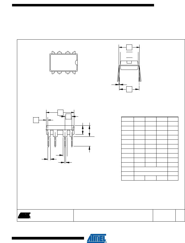
Packaging Information
8P3
1 |
E |
|

 E1
E1 

|
N |
Top View |
c |
|
eA |
|
End View |
D
e
D1 |
A2 A |
 b2 L
b2 L
b3
4 PLCS |
b |
Side View
COMMON DIMENSIONS
(Unit of Measure = inches)
SYMBOL |
MIN |
NOM |
MAX |
NOTE |
A |
|
|
0.210 |
2 |
A2 |
0.115 |
0.130 |
0.195 |
|
b |
0.014 |
0.018 |
0.022 |
5 |
b2 |
0.045 |
0.060 |
0.070 |
6 |
b3 |
0.030 |
0.039 |
0.045 |
6 |
c |
0.008 |
0.010 |
0.014 |
|
D |
0.355 |
0.365 |
0.400 |
3 |
D1 |
0.005 |
|
|
3 |
E |
0.300 |
0.310 |
0.325 |
4 |
E1 |
0.240 |
0.250 |
0.280 |
3 |
e |
|
0.100 BSC |
|
|
eA |
|
0.300 BSC |
|
4 |
L |
0.115 |
0.130 |
0.150 |
2 |
Notes: 1. This drawing is for general information only; refer to JEDEC Drawing MS-001, Variation BA for additional information.
2.Dimensions A and L are measured with the package seated in JEDEC seating plane Gauge GS-3.
3.D, D1 and E1 dimensions do not include mold Flash or protrusions. Mold Flash or protrusions shall not exceed 0.010 inch.
4.E and eA measured with the leads constrained to be perpendicular to datum.
5.Pointed or rounded lead tips are preferred to ease insertion.
6.b2 and b3 maximum dimensions do not include Dambar protrusions. Dambar protrusions shall not exceed 0.010 (0.25 mm).
|
|
01/09/02 |
||
|
TITLE |
DRAWING NO. |
REV. |
|
2325 Orchard Parkway |
8P3, 8-lead, 0.300" Wide Body, Plastic Dual |
8P3 |
B |
|
R San Jose, CA 95131 |
In-line Package (PDIP) |
|||
|
|
|||
89
1006F–AVR–06/07
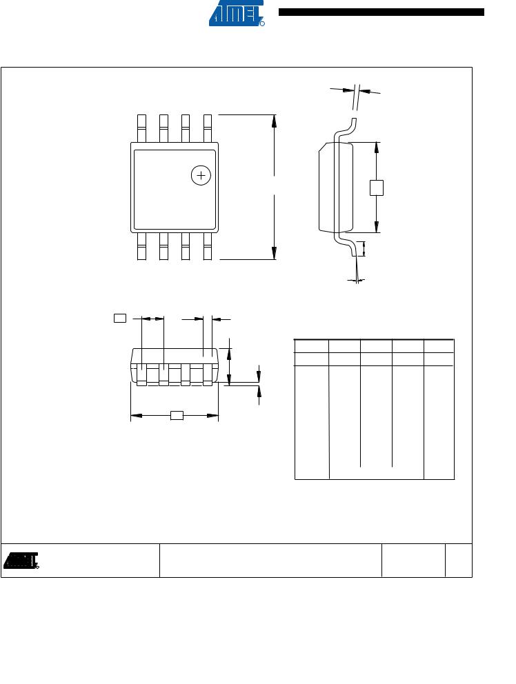
8S2
C
1
E |
E1 |
L
|
N |
TOP VIEW |
θ |
|
END VIEW |
e
D |
SIDE VIEW
b |
|
COMMON DIMENSIONS |
|
||
|
|
|
|||
A |
|
(Unit of Measure = mm) |
|
||
|
SYMBOL |
MIN |
NOM |
MAX |
NOTE |
A1 |
A |
1.70 |
|
2.16 |
|
|
|
|
|||
|
A1 |
0.05 |
0.25 |
|
|
|
b |
0.35 |
0.48 |
5 |
|
|
|
|
|
|
|
|
C |
0.15 |
0.35 |
5 |
|
|
|
|
|
|
|
|
D |
5.13 |
5.35 |
|
|
|
|
|
|
|
|
|
E1 |
5.18 |
5.40 |
2, 3 |
|
|
|
|
|
|
|
|
E |
7.70 |
8.26 |
|
|
|
|
|
|
|
|
|
L |
0.51 |
0.85 |
|
|
|
|
|
|
|
|
|
θ |
0° |
8° |
|
|
|
e |
|
1.27 BSC |
4 |
|
Notes: 1. This drawing is for general information only; refer to EIAJ Drawing EDR-7320 for additional information. 2. Mismatch of the upper and lower dies and resin burrs are not included.
3. It is recommended that upper and lower cavities be equal. If they are different, the larger dimension shall be regarded.
4.Determines the true geometric position.
5.Values b,C apply to plated terminal. The standard thickness of the plating layer shall measure between 0.007 to .021 mm.
|
|
|
4/7/06 |
|
|
TITLE |
DRAWING NO. |
REV. |
|
2325 Orchard Parkway |
8S2, 8-lead, 0.209" Body, Plastic Small |
8S2 |
D |
|
R San Jose, CA 95131 |
Outline Package (EIAJ) |
|||
|
|
90 ATtiny11/12 
1006F–AVR–06/07
 ATtiny11/12
Datasheet Revision
History
Rev. 1006F-06/07
Rev. 1006E-07/06
Rev. 1006D-07/03
Rev. 1006C-09/01
Please note that the page numbers listed in this section are refering to this document. The revision numbers are referring to the document revision.
1. “Not recommended for new design”.
1.Updated chapter layout.
2.Updated Power-down in “Sleep Modes for the ATtiny11” on page 20.
3.Updated Power-down in “Sleep Modes for the ATtiny12” on page 20.
4.Updated Table 16 on page 36.
5.Updated “Calibration Byte in ATtiny12” on page 49.
6.Updated “Ordering Information” on page 87.
7.Updated “Packaging Information” on page 89.
1. Updated VBOT values in Table 9 on page 24.
1. N/A
91
1006F–AVR–06/07

|
|
ATtiny11/12 |
Table of Contents |
Features........................................................................................ |
......... 1 |
|
Pin Configuration......................................................................... |
......... 1 |
|
Description ................................................................................... |
......... 2 |
|
ATtiny11 Block Diagram ....................................................................................... |
2 |
|
ATtiny12 Block Diagram ....................................................................................... |
4 |
|
Pin Descriptions.................................................................................................... |
5 |
|
Clock Options ....................................................................................................... |
5 |
|
Architectural Overview................................................................ |
......... 8 |
|
General-purpose Register File.............................................................................. |
9 |
|
ALU – Arithmetic Logic Unit................................................................................ |
10 |
|
Flash Program Memory ...................................................................................... |
10 |
|
Program and Data Addressing Modes................................................................ |
10 |
|
Subroutine and Interrupt Hardware Stack .......................................................... |
12 |
|
EEPROM Data Memory...................................................................................... |
13 |
|
Memory Access and Instruction Execution Timing ............................................. |
13 |
|
I/O Memory ......................................................................................................... |
14 |
|
Reset and Interrupt Handling.............................................................................. |
15 |
|
ATtiny12 Internal Voltage Reference.................................................................. |
24 |
|
Interrupt Handling ............................................................................................... |
25 |
|
Sleep Modes for the ATtiny11 ............................................................................ |
31 |
|
Sleep Modes for the ATtiny12 ............................................................................ |
31 |
|
ATtiny12 Calibrated Internal RC Oscillator ......................................................... |
32 |
|
Timer/Counter0 .......................................................................... |
......... 33 |
|
Timer/Counter Prescaler..................................................................................... |
33 |
|
Watchdog Timer......................................................................... |
......... 36 |
|
ATtiny12 EEPROM Read/Write Access...................................... |
....... 38 |
|
Prevent EEPROM Corruption ............................................................................. |
40 |
|
Analog Comparator ................................................................ |
............ 41 |
|
I/O Port B .................................................................................... |
......... 43 |
|
Memory Programming............................................................ |
............ 46 |
|
Program (and Data) Memory Lock Bits .............................................................. |
46 |
|
Fuse Bits in ATtiny11.......................................................................................... |
46 |
|
Fuse Bits in ATtiny12.......................................................................................... |
46 |
|
Signature Bytes .................................................................................................. |
47 |
|
Calibration Byte in ATtiny12 ............................................................................... |
47 |
|
Programming the Flash and EEPROM............................................................... |
47 |
|
High-voltage Serial Programming....................................................................... |
48 |
|
|
i |
1006F–AVR–06/07 |
|
|

High-voltage Serial Programming Algorithm....................................................... |
49 |
High-voltage Serial Programming Characteristics .............................................. |
52 |
Low-voltage Serial Downloading (ATtiny12 only) ............................................... |
52 |
Low-voltage Serial Programming Characteristics............................................... |
56 |
Electrical Characteristics................................................................... |
57 |
Absolute Maximum Ratings ................................................................................ |
57 |
DC Characteristics – Preliminary Data ............................................................... |
57 |
External Clock Drive Waveforms ........................................................................ |
59 |
External Clock Drive ATtiny11 ............................................................................ |
59 |
External Clock Drive ATtiny12 ............................................................................ |
59 |
ATtiny11 Typical Characteristics ........................................................................ |
60 |
ATtiny12 Typical Characteristics ........................................................................ |
72 |
Register Summary ATtiny11.............................................................. |
81 |
Register Summary ATtiny12.............................................................. |
82 |
Instruction Set Summary ................................................................... |
83 |
Ordering Information.......................................................................... |
85 |
Packaging Information ....................................................................... |
86 |
8P3 ..................................................................................................................... |
86 |
8S2 ..................................................................................................................... |
87 |
Data Sheet Change Log for Chip Number ........................................ |
88 |
Changes from Rev. 1006C-09/01 to Rev. 1006D-07/03..................................... |
88 |
Table of Contents .................................................................................. |
i |
ii ATtiny11/12
1006F–AVR–06/07

Headquarters |
International |
|
|
|
|
|
|
|
|
Atmel Corporation |
|
Atmel Asia |
Atmel Europe |
Atmel Japan |
2325 Orchard Parkway |
|
Room 1219 |
Le Krebs |
9F, Tonetsu Shinkawa Bldg. |
San Jose, CA 95131 |
|
Chinachem Golden Plaza |
8, Rue Jean-Pierre Timbaud |
1-24-8 Shinkawa |
USA |
|
77 Mody Road Tsimshatsui |
BP 309 |
Chuo-ku, Tokyo 104-0033 |
Tel: 1(408) 441-0311 |
|
East Kowloon |
78054 Saint-Quentin-en- |
Japan |
Fax: 1(408) 487-2600 |
|
Hong Kong |
Yvelines Cedex |
Tel: (81) 3-3523-3551 |
|
|
Tel: (852) 2721-9778 |
France |
Fax: (81) 3-3523-7581 |
|
|
Fax: (852) 2722-1369 |
Tel: (33) 1-30-60-70-00 |
|
|
|
|
Fax: (33) 1-30-60-71-11 |
|
Product Contact
Web Site |
Technical Support |
Sales Contact |
www.atmel.com |
Enter Product Line E-mail |
www.atmel.com/contacts |
Literature Requests |
|
|
www.atmel.com/literature |
|
|
Disclaimer: The information in this document is provided in connection with Atmel products. No license, express or implied, by estoppel or otherwise, to any intellectual property right is granted by this document or in connection with the sale of Atmel products. EXCEPT AS SET FORTH IN ATMEL’S TERMS AND CONDI-
TIONS OF SALE LOCATED ON ATMEL’S WEB SITE, ATMEL ASSUMES NO LIABILITY WHATSOEVER AND DISCLAIMS ANY EXPRESS, IMPLIED OR STATUTORY WARRANTY RELATING TO ITS PRODUCTS INCLUDING, BUT NOT LIMITED TO, THE IMPLIED WARRANTY OF MERCHANTABILITY, FITNESS FOR A PARTICULAR PURPOSE, OR NON-INFRINGEMENT. IN NO EVENT SHALL ATMEL BE LIABLE FOR ANY DIRECT, INDIRECT, CONSEQUENTIAL, PUNITIVE, SPECIAL OR INCIDENTAL DAMAGES (INCLUDING, WITHOUT LIMITATION, DAMAGES FOR LOSS OF PROFITS, BUSINESS INTERRUPTION, OR LOSS OF INFORMATION) ARISING OUT OF THE USE OR INABILITY TO USE THIS DOCUMENT, EVEN IF ATMEL HAS BEEN ADVISED OF THE POSSIBILITY OF SUCH DAMAGES. Atmel makes no representations or warranties with respect to the accuracy or completeness of the contents of this document and reserves the right to make changes to specifications and product descriptions at any time without notice. Atmel does not make any commitment to update the information contained herein. Unless specifically provided otherwise, Atmel products are not suitable for, and shall not be used in, automotive applications. Atmel’s products are not intended, authorized, or warranted for use as components in applications intended to support or sustain life.
© 2006 Atmel Corporation. All rights reserved. Atmel®, logo and combinations thereof, are the registered trademarks of Atmel Corporation or its subsidiaries. Other terms and product names may be trademarks of others.
1006F–AVR–06/07