

|
|
|
|
|
|
|
|
|
|
|
|
|
ATtiny11/12 |
||
|
|
|
|
|
|
|
|
|
|
|
|
|
|||
|
Timer/Counter0 |
|
|
|
|
|
|
|
|
|
|
|
|||
|
The ATtiny11/12 provides one general-purpose 8-bit Timer/Counter – Timer/Counter0. |
||||||||||||||
|
|||||||||||||||
|
|
The Timer/Counter0 has prescaling selection from the 10-bit prescaling timer. The |
|||||||||||||
|
|
Timer/Counter0 can either be used as a timer with an internal clock timebase or as a |
|||||||||||||
|
|
counter with an external pin connection that triggers the counting. |
|||||||||||||
|
Timer/Counter Prescaler |
Figure 22 shows the Timer/Counter prescaler. |
|
|
|
|
|
||||||||
|
|
Figure 22. Timer/Counter0 Prescaler |
|
|
|
|
|
|
|
|
|||||
|
|
CK |
|
|
|
|
|
|
|
|
|
|
|
|
|
|
|
|
|
|
|
|
|
10-BIT T/C PRESCALER |
|
|
|
|
|
||
|
|
|
|
|
|
|
|
|
|
|
|||||
|
|
|
|
|
|
|
|
|
|
|
|
|
|
|
|
|
|
|
|
|
|
|
CK/8 |
|
|
CK/64 |
CK/256 |
|
CK/1024 |
||
|
|
|
|
|
|
|
|
|
|
|
|
|
|||
|
|
T0 |
|
|
|
|
|
|
|
|
|
||||
|
|
|
0 |
|
|
|
|
|
|
||||||
|
|
|
|
|
|
|
|
|
|
|
|
|
|
||
|
|
CS00 |
|
|
|
|
|
|
|
|
|||||
|
|
|
|
|
|
|
|
|
|
||||||
|
|
CS01 |
|
|
|
|
|
|
|
|
|||||
|
|
CS02 |
|
|
|
|
|
|
|
|
|||||
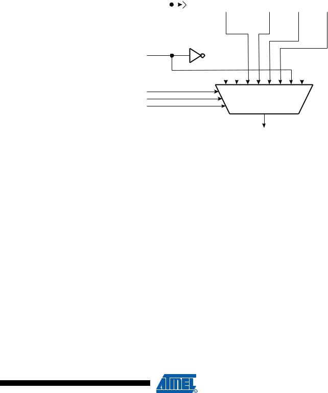
TIMER/COUNTER0 CLOCK SOURCE
TCK0
The four different prescaled selections are: CK/8, CK/64, CK/256 and CK/1024 where CK is the oscillator clock. CK, external source and stop, can also be selected as clock sources.
Figure 23 shows the block diagram for Timer/Counter0.
The 8-bit Timer/Counter0 can select clock source from CK, prescaled CK, or an external pin. In addition, it can be stopped as described in the specification for the Timer/Counter0 Control Register – TCCR0. The overflow status flag is found in the Timer/Counter Interrupt Flag Register – TIFR. Control signals are found in the Timer/Counter0 Control Register – TCCR0. The interrupt enable/disable settings for Timer/Counter0 are found in the Timer/Counter Interrupt Mask Register – TIMSK.
When Timer/Counter0 is externally clocked, the external signal is synchronized with the oscillator frequency of the CPU. To ensure proper sampling of the external clock, the minimum time between two external clock transitions must be at least one internal CPU clock period. The external clock signal is sampled on the rising edge of the internal CPU clock.
The 8-bit Timer/Counter0 features both a high-resolution and a high-accuracy usage with the lower prescaling opportunities. Similarly, the high-prescaling opportunities make the Timer/Counter0 useful for lower-speed functions or exact-timing functions with infrequent actions.
39
1006F–AVR–06/07

Figure 23. Timer/Counter0 Block Diagram
T0 |
40 ATtiny11/12
1006F–AVR–06/07