

ADSP-2191M
The two address buses (PMA and DMA) share a single external address bus, allowing memory to be expanded off-chip, and the two data buses (PMD and DMD) share a single external data bus. Boot memory space and I/O memory space also share the external buses.
Program memory can store both instructions and data, permitting the ADSP-2191M to fetch two operands in a single cycle, one from program memory and one from data memory. The DSP’s dual memory buses also let the ADSP-219x core fetch an operand from data memory and the next instruction from program memory in a single cycle.
DSP Peripherals Architecture
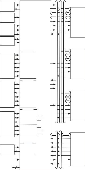
The functional block diagram on Page 1 shows the DSP’s on-chip peripherals, which include the external memory interface, Host port, serial ports, SPI-compatible ports, UART port, JTAG test and emulation port, timers, flags, and interrupt controller. These on-chip peripherals can connect to off-chip devices as shown in Figure 1.
The ADSP-2191M has a 16-bit Host port with DMA capability that lets external Hosts access on-chip memory. This 24-pin parallel port consists of a 16-pin multiplexed data/address bus and provides a lowservice overhead data move capability. Configurable for 8 or 16 bits, this port provides a glueless interface to a wide variety of 8- and 16-bit microcontrollers. Two chip-selects provide Hosts access to the DSP’s entire memory map. The DSP is bootable through this port.
The ADSP-2191M also has an external memory interface that is shared by the DSP’s core, the DMA controller, and DMA capable peripherals, which include the UART, SPORT0, SPORT1, SPORT2, SPI0, SPI1, and the Host port. The external port consists of a 16-bit data bus, a 22-bit address bus, and control signals. The data bus is configurable to provide an 8- or 16-bit interface to external memory. Support for word packing lets the DSP access 16or 24-bit words from external memory regardless of the external data bus width. When configured for an 8-bit interface, the unused eight lines provide eight programmable, bidirectional general-purpose Programmable Flag lines, six of which can be mapped to software condition signals.
The memory DMA controller lets the ADSP-2191M move data and instructions from between memory spaces: internal-to-exter- nal, internal-to-internal, and external-to-external. On-chip peripherals can also use this controller for DMA transfers.
The ADSP-2191M can respond to up to seventeen interrupts at any given time: three internal (stack, emulator kernel, and power-down), two external (emulator and reset), and twelve userdefined (peripherals) interrupts. The programmer assigns a peripheral to one of the 12 user-defined interrupts. The priority of each peripheral for interrupt service is determined by these assignments.
There are three serial ports on the ADSP-2191M that provide a complete synchronous, full-duplex serial interface. This interface includes optional companding in hardware as well as a wide variety of framed or frameless data transmit and receive modes
|
ADSP-2191M |
|
|
EXTERNAL |
||
CLOCK |
|
|
|
|
MEMORY |
|
CLKIN |
CLKOUT |
|
|
(OPTIONAL) |
||
OR |
|
|
|
|||
XTAL |
ADDR21–0 |
|
|
ADDR21–0 |
||
CRYSTAL |
|
|
||||
TIMER |
|
DATA15–8 |
|
|
DATA15–8 |
|
TMR2–0 |
DATA7–0 |
|
|
DATA7–0 |
||
OUT OR |
|
|
||||
CAPTURE |
|
MS3–0 |
|
|
CS |
|
|
|
|
|
|||
CLOCK |
MSEL6–0/PF6–0 |
RD |
|
|
OE |
|
MULTIPLY |
DF/PF7 |
WR |
|
|
WE |
|
AND |
|
|
||||
|
|
|
|
|
||
RANGE |
BYPASS |
ACK |
|
|
ACK |
|
BOOT |
BMODE1–0 |
CONTROL |
ADDRESS |
|
|
|
AND OP |
OPMODE |
DATA |
BOOT |
|||
MODE |
MEMORY |
|||||
|
||||||
|
|
(OPTIONAL) |
||||
|
|
|
||||
|
SPORT0 |
|
|
|
ADDR21–0 |
|
|
TCLK0 |
|
|
|
DATA15–8 |
|
|
TFS0 |
|
|
|
DATA7–0 |
|
SERIAL |
DT0 |
BMS |
|
|
CS |
|
DEVICE |
RCLK0 |
|
|
|
OE |
|
(OPTIONAL) |
|
|
|
|||
|
RFS0 |
|
|
|
WE |
|
|
DR0 |
|
|
|
ACK |
|
|
SPORT1 |
BR |
|
|
EXTERNAL |
|
|
TCLK1 |
BG |
|
|
||
|
|
|
I/O MEMORY |
|||
|
|
|
|
|
||
|
TFS1 |
BGH |
|
|
(OPTIONAL) |
|
SERIAL |
DT1 |
|
|
|
ADDR17–0 |
|
DEVICE |
RCLK1 |
|
|
|
DATA15–8 |
|
(OPTIONAL) |
|
|
|
|||
|
RFS1 |
|
|
|
DATA7–0 |
|
|
DR1 |
IOMS |
|
|
CS |
|
|
SPORT2 |
|
|
|
OE |
|
|
TCLK2/SCK0 |
|
|
|
WE |
|
|
TFS2/MOSI0 |
SPI0 |
|
|
ACK |
|
SERIAL |
DT2/MISO0 |
|
|
|
|
|
DEVICE |
RCLK2/SCK1 |
|
|
|
HOST |
|
(OPTIONAL) |
|
|
|
PROCESSOR |
||
|
|
|
|
|||
|
RFS2/MOSI1 |
SPI1 |
|
|
(OPTIONAL) |
|
|
DR2/MISO1 |
HAD15–0 |
|
|
ADDR15–0/ |
|
|
|
HA16 |
|
|
DATA15–0 |
|
|
|
|
|
ADDR16 |
||
|
|
|
|
|
||
|
UART |
HCMS |
|
|
CS0 |
|
UART |
RXD |
HCIOMS |
|
|
CS1 |
|
DEVICE |
TXD |
HRD |
|
|
RD |
|
(OPTIONAL) |
|
|
||||
|
|
HWR |
|
|
WR |
|
|
RESET |
HACK |
|
|
ACK |
|
|
6 |
HALE |
|
|
ALE |
|
|
HACK_P |
|
|
|
||
|
JTAG |
|
|
|
||
Figure 1. System Diagram
of operation. Each serial port can transmit or receive an internal or external, programmable serial clock and frame syncs. Each serial port supports 128-channel Time Division Multiplexing.
The ADSP-2191M provides up to sixteen general-purpose I/O pins, which are programmable as either inputs or outputs. Eight of these pins are dedicated-general purpose Programmable Flag pins. The other eight of them are multifunctional pins, acting as general-purpose I/O pins when the DSP connects to an 8-bit external data bus and acting as the upper eight data pins when the DSP connects to a 16-bit external data bus. These Programmable Flag pins can implement edgeor level-sensitive interrupts, some of which can be used to base the execution of conditional instructions.
–4– |
REV. A |