

a |
ADSP-2100 Family |
|
DSP Microcomputers |
||
|
|
|
|
|
ADSP-21xx |
|
|
|
SUMMARY
16-Bit Fixed-Point DSP Microprocessors with On-Chip Memory
Enhanced Harvard Architecture for Three-Bus Performance: Instruction Bus & Dual Data Buses
Independent Computation Units: ALU, Multiplier/ Accumulator, and Shifter
Single-Cycle Instruction Execution & Multifunction Instructions
On-Chip Program Memory RAM or ROM & Data Memory RAM
Integrated I/O Peripherals: Serial Ports, Timer, Host Interface Port (ADSP-2111 Only)
FEATURES
25 MIPS, 40 ns Maximum Instruction Rate
Separate On-Chip Buses for Program and Data Memory Program Memory Stores Both Instructions and Data
(Three-Bus Performance)
Dual Data Address Generators with Modulo and Bit-Reverse Addressing
Efficient Program Sequencing with Zero-Overhead Looping: Single-Cycle Loop Setup
Automatic Booting of On-Chip Program Memory from Byte-Wide External Memory (e.g., EPROM )
Double-Buffered Serial Ports with Companding Hardware, Automatic Data Buffering, and Multichannel Operation ADSP-2111 Host Interface Port Provides Easy Interface
to 68000, 80C51, ADSP-21xx, Etc.
Automatic Booting of ADSP-2111 Program Memory Through Host Interface Port
Three Edgeor Level-Sensitive Interrupts Low Power IDLE Instruction
PGA, PLCC, PQFP, and TQFP Packages MIL-STD-883B Versions Available
GENERAL DESCRIPTION
The ADSP-2100 Family processors are single-chip microcomputers optimized for digital signal processing (DSP) and other high speed numeric processing applications. The
ADSP-21xx processors are all built upon a common core. Each processor combines the core DSP architecture—computation units, data address generators, and program sequencer—with differentiating features such as on-chip program and data memory RAM, a programmable timer, one or two serial ports, and, on the ADSP-2111, a host interface port.
REV. B
Information furnished by Analog Devices is believed to be accurate and reliable. However, no responsibility is assumed by Analog Devices for its use, nor for any infringements of patents or other rights of third parties which may result from its use. No license is granted by implication or otherwise under any patent or patent rights of Analog Devices.
|
FUNCTIONAL BLOCK DIAGRAM |
||||
DATA ADDRESS |
|
MEMORY |
|
FLAGS |
|
PROGRAM |
|
|
DATA |
(ADSP-2111) |
|
GENERATORS |
PROGRAM |
|
|||
|
|
||||
DAG 1 DAG 2 |
SEQUENCER |
MEMORY |
MEMORY |
|
|
|
|
|
|
EXTERNAL |
|
|
|
|
|
|
|
|
|
|
|
|
ADDRESS |
|
PROGRAM MEMORY ADDRESS |
|
|
BUS |
|
|
|
|
|
||
DATA MEMORY ADDRESS
PROGRAM MEMORY DATA
DATA MEMORY DATA
|
|
|
EXTERNAL |
|
|
|
DATA |
|
|
|
BUS |
ARITHMETIC UNITS |
SERIAL PORTS |
TIMER |
HOST |
|
|
|
INTERFACE |
ALU MAC SHIFTER |
SPORT 0 SPORT 1 |
|
PORT |
|
|
|
(ADSP-2111) |
ADSP-2100 CORE
This data sheet describes the following ADSP-2100 Family processors:
ADSP-2101 |
|
ADSP-2103 |
3.3 V Version of ADSP-2101 |
ADSP-2105 |
Low Cost DSP |
ADSP-2111 |
DSP with Host Interface Port |
ADSP-2115 |
|
ADSP-2161/62/63/64 |
Custom ROM-programmed DSPs |
The following ADSP-2100 Family processors are not included in this data sheet:
ADSP-2100A |
DSP Microprocessor |
ADSP-2165/66 ROM-programmed ADSP-216x processors with powerdown and larger on-chip memories (12K Program Memory ROM, 1K Program Memory RAM, 4K Data Memory RAM)
ADSP-21msp5x Mixed-Signal DSP Processors with integrated on-chip A/D and D/A plus powerdown
ADSP-2171 |
Speed and feature enhanced ADSP-2100 |
|
Family processor with host interface port, |
|
powerdown, and instruction set extensions |
|
for bit manipulation, multiplication, biased |
|
rounding, and global interrupt masking |
ADSP-2181 |
ADSP-21xx processor with ADSP-2171 |
|
features plus 80K bytes of on-chip RAM |
|
configured as 16K words of program |
|
memory and 16K words of data memory. |
Refer to the individual data sheet of each of these processors for further information.
© Analog Devices, Inc., 1996
One Technology Way, P.O. Box 9106, Norwood, MA 02062-9106, U.S.A. Tel: 617/329-4700 Fax: 617/326-8703

ADSP-21xx
Fabricated in a high speed, submicron, double-layer metal CMOS process, the highest-performance ADSP-21xx processors operate at 25 MHz with a 40 ns instruction cycle time. Every instruction can execute in a single cycle. Fabrication in CMOS results in low power dissipation.
The ADSP-2100 Family’s flexible architecture and comprehensive instruction set support a high degree of parallelism. In one cycle the ADSP-21xx can perform all of the following operations:
•Generate the next program address
•Fetch the next instruction
•Perform one or two data moves
•Update one or two data address pointers
•Perform a computation
•Receive and transmit data via one or two serial ports
•Receive and/or transmit data via the host interface port (ADSP-2111 only)
The ADSP-2101, ADSP-2105, and ADSP-2115 comprise the basic set of processors of the family. Each of these three devices contains program and data memory RAM, an interval timer, and one or two serial ports. The ADSP-2103 is a 3.3 volt power supply version of the ADSP-2101; it is identical to the ADSP-2101 in all other characteristics. Table I shows the features of each ADSP-21xx processor.
The ADSP-2111 adds a 16-bit host interface port (HIP) to the basic set of ADSP-21xx integrated features. The host port provides a simple interface to host microprocessors or microcontrollers such as the 8031, 68000, or ISA bus.
TABLE OF CONTENTS
GENERAL DESCRIPTION . . . . . . . . . . . . . . . . . . . . . . . . 1
Development Tools . . . . . . . . . . . . . . . . . . . . . . . . . . . . . . . 4
Additional Information . . . . . . . . . . . . . . . . . . . . . . . . . . . . 4
ARCHITECTURE OVERVIEW . . . . . . . . . . . . . . . . . . . . 4 Serial Ports . . . . . . . . . . . . . . . . . . . . . . . . . . . . . . . . . . . . . 5 Host Interface Port (ADSP-2111) . . . . . . . . . . . . . . . . . . . . 6 Interrupts . . . . . . . . . . . . . . . . . . . . . . . . . . . . . . . . . . . . . . . 6 Pin Definitions . . . . . . . . . . . . . . . . . . . . . . . . . . . . . . . . . . . 7 SYSTEM INTERFACE . . . . . . . . . . . . . . . . . . . . . . . . . . . 7 Clock Signals . . . . . . . . . . . . . . . . . . . . . . . . . . . . . . . . . . . . 7 Reset . . . . . . . . . . . . . . . . . . . . . . . . . . . . . . . . . . . . . . . . . . 8 Program Memory Interface . . . . . . . . . . . . . . . . . . . . . . . . 10 Program Memory Maps . . . . . . . . . . . . . . . . . . . . . . . . . . . 10 Data Memory Interface . . . . . . . . . . . . . . . . . . . . . . . . . . . 12 Data Memory Map . . . . . . . . . . . . . . . . . . . . . . . . . . . . . . 12 Boot Memory Interface . . . . . . . . . . . . . . . . . . . . . . . . . . . 12 Bus Interface . . . . . . . . . . . . . . . . . . . . . . . . . . . . . . . . . . . 12 Low Power IDLE Instruction . . . . . . . . . . . . . . . . . . . . . . 13 ADSP-216x Prototyping . . . . . . . . . . . . . . . . . . . . . . . . . . 13 Ordering Procedure for ADSP-216x ROM Processors . . . . 13 Wafer Products . . . . . . . . . . . . . . . . . . . . . . . . . . . . . . . . . 14 Functional Differences for Older Revision Devices . . . . . . 14 Instruction Set . . . . . . . . . . . . . . . . . . . . . . . . . . . . . . . . . . 15
SPECIFICATIONS
(ADSP-2101/2105/2115/2161/2163) . . . . . . . . . . . . . . . 17 Recommended Operating Conditions . . . . . . . . . . . . . . . . 17 Electrical Characteristics . . . . . . . . . . . . . . . . . . . . . . . . . . 17 Supply Current & Power (ADSP-2101/2161/2163) . . . . . . 18 Power Dissipation Example . . . . . . . . . . . . . . . . . . . . . . . . 19 Environmental Conditions . . . . . . . . . . . . . . . . . . . . . . . . . 19 Capacitive Loading . . . . . . . . . . . . . . . . . . . . . . . . . . . . . . 19 Test Conditions . . . . . . . . . . . . . . . . . . . . . . . . . . . . . . . . . 20
SPECIFICATIONS
(ADSP-2111) . . . . . . . . . . . . . . . . . . . . . . . . . . . . . . . . . 21 Recommended Operating Conditions . . . . . . . . . . . . . . . . 21 Electrical Characteristics . . . . . . . . . . . . . . . . . . . . . . . . . . 21 Supply Current & Power . . . . . . . . . . . . . . . . . . . . . . . . . . 22 Power Dissipation Example . . . . . . . . . . . . . . . . . . . . . . . . 23 Environmental Conditions . . . . . . . . . . . . . . . . . . . . . . . . . 23
Capacitive Loading . . . . . . . . . . . . . . . . . . . . . . . . . . . . . . 23
Test Conditions . . . . . . . . . . . . . . . . . . . . . . . . . . . . . . . . . 24
SPECIFICATIONS (ADSP-2103/2162/2164) . . . . . . . . . 25
Recommended Operating Conditions . . . . . . . . . . . . . . . . 25
Electrical Characteristics . . . . . . . . . . . . . . . . . . . . . . . . . . 25
Supply Current & Power . . . . . . . . . . . . . . . . . . . . . . . . . . 26
Power Dissipation Example . . . . . . . . . . . . . . . . . . . . . . . . 27
Environmental Conditions . . . . . . . . . . . . . . . . . . . . . . . . . 27
Capacitive Loading . . . . . . . . . . . . . . . . . . . . . . . . . . . . . . 27
Test Conditions . . . . . . . . . . . . . . . . . . . . . . . . . . . . . . . . . 28
TIMING PARAMETERS (ADSP-2101/2105/2111/2115/2161/2163) . . . . . . . . . . . . 29
Clock Signals . . . . . . . . . . . . . . . . . . . . . . . . . . . . . . . . . . . 30 Interrupts & Flags . . . . . . . . . . . . . . . . . . . . . . . . . . . . . . . 31 Bus Request–Bus Grant . . . . . . . . . . . . . . . . . . . . . . . . . . . 32 Memory Read . . . . . . . . . . . . . . . . . . . . . . . . . . . . . . . . . . 33 Memory Write . . . . . . . . . . . . . . . . . . . . . . . . . . . . . . . . . . 34 Serial Ports . . . . . . . . . . . . . . . . . . . . . . . . . . . . . . . . . . . . 35 Host Interface Port (ADSP-2111) . . . . . . . . . . . . . . . . . . . 36
TIMING PARAMETERS (ADSP-2103/2162/2164) . . . . 44
Clock Signals . . . . . . . . . . . . . . . . . . . . . . . . . . . . . . . . . . . 45
Interrupts & Flags . . . . . . . . . . . . . . . . . . . . . . . . . . . . . . . 46
Bus Request–Bus Grant . . . . . . . . . . . . . . . . . . . . . . . . . . . 47
Memory Read . . . . . . . . . . . . . . . . . . . . . . . . . . . . . . . . . . 48
Memory Write . . . . . . . . . . . . . . . . . . . . . . . . . . . . . . . . . . 49
Serial Ports . . . . . . . . . . . . . . . . . . . . . . . . . . . . . . . . . . . . 50
PIN CONFIGURATIONS
68-Pin PGA (ADSP-2101) . . . . . . . . . . . . . . . . . . . . . . . . 51
68-Lead PLCC (ADSP-2101/2103/2105/2115/216x) . . . . 52
80-Lead PQFP (ADSP-2101/2103/2115/216x) . . . . . . . . . 53
80-Lead TQFP (ADSP-2115) . . . . . . . . . . . . . . . . . . . . . . 53
100-Pin PGA (ADSP-2111) . . . . . . . . . . . . . . . . . . . . . . . 54
100-Lead PQFP (ADSP-2111) . . . . . . . . . . . . . . . . . . . . . 55
PACKAGE OUTLINE DIMENSIONS
68-Pin PGA . . . . . . . . . . . . . . . . . . . . . . . . . . . . . . . . . . . . 56
68-Lead PLCC . . . . . . . . . . . . . . . . . . . . . . . . . . . . . . . . . 57
80-Lead PQFP, 80-Lead TQFP . . . . . . . . . . . . . . . . . . . . 58
100-Pin PGA . . . . . . . . . . . . . . . . . . . . . . . . . . . . . . . . . . . 59
100-Lead PQFP . . . . . . . . . . . . . . . . . . . . . . . . . . . . . . . . 60
ORDERING GUIDE . . . . . . . . . . . . . . . . . . . . . . . . . . 61-62
–2– |
REV. B |

ADSP-21xx
Table I. ADSP-21xx Processor Features
Feature |
|
|
|
2101 |
|
2103 |
|
2105 |
|
2115 |
|
2111 |
||||||
|
|
|
|
|
|
|
|
|
|
|
|
|
|
|
|
|
||
Data Memory (RAM) |
|
1K |
|
1K |
|
1⁄2 K |
|
1⁄2 K |
|
1K |
||||||||
Program Memory (RAM) |
|
2K |
|
2K |
|
1K |
|
1K |
|
2K |
||||||||
Timer |
|
|
|
• |
|
• |
|
• |
|
• |
|
• |
||||||
Serial Port 0 (Multichannel) |
|
• |
|
• |
|
– |
|
• |
|
• |
||||||||
Serial Port 1 |
|
|
|
• |
|
• |
|
• |
|
• |
|
• |
||||||
Host Interface Port |
|
|
– |
|
– |
|
– |
|
– |
|
• |
|||||||
|
|
|
|
|
|
|
|
|||||||||||
Speed Grades (Instruction Cycle Time) |
|
|
|
|
• |
|
|
|
|
|
|
|
|
|
||||
|
10.24 MHz (76.9 ns) |
|
– |
|
|
– |
|
– |
|
– |
||||||||
|
13.0 MHz (76.9 ns) |
|
– |
|
– |
|
– |
|
– |
|
• |
|||||||
|
13.824 MHz (72.3 ns) |
|
– |
|
– |
|
• |
|
– |
|
– |
|||||||
|
16.67 MHz (60 ns) |
|
• |
|
– |
|
– |
|
• |
|
• |
|||||||
|
20.0 MHz (50 ns) |
|
|
• |
|
– |
|
• |
|
• |
|
• |
||||||
|
25 MHz (40 ns) |
|
|
• |
|
– |
|
– |
|
• |
|
– |
||||||
Supply Voltage |
|
|
|
5 V |
|
3.3 V |
|
5 V |
|
5 V |
|
5 V |
||||||
Packages |
|
|
|
• |
|
|
|
|
|
|
|
|
|
|
|
|
||
|
68-Pin PGA |
|
|
|
|
– |
|
– |
|
– |
|
– |
||||||
|
|
|
|
• |
|
|
|
|
||||||||||
|
68-Lead PLCC |
|
|
|
|
• |
|
• |
|
• |
|
– |
||||||
|
80-Lead PQFP |
|
|
|
• |
|
• |
|
– |
|
• |
|
– |
|||||
|
80-Lead TQFP |
|
|
|
– |
|
– |
|
– |
|
• |
|
– |
|||||
|
100-Pin PGA |
|
|
|
– |
|
– |
|
– |
|
– |
|
• |
|||||
|
100-Lead PQFP |
|
|
– |
|
– |
|
– |
|
– |
|
• |
||||||
|
|
|
|
|
|
|
|
|
||||||||||
Temperature Grades |
|
|
• |
|
• |
|
• |
|
• |
|
• |
|||||||
|
K Commercial |
0°C to +70°C |
|
|
|
|
|
|||||||||||
|
|
• |
|
• |
|
• |
|
• |
|
• |
||||||||
|
B Industrial –40°C to +85°C |
|
|
|
|
|
||||||||||||
|
T Extended |
–55°C to +125°C |
|
• |
|
– |
|
– |
|
– |
|
• |
||||||
|
|
|
|
|
|
|
|
|
|
|||||||||
|
|
|
|
|
|
|
|
|
|
|
|
|
||||||
|
Table II. ADSP-216x ROM-Programmed Processor Features |
|
|
|||||||||||||||
|
|
|
|
|
|
|
|
|
|
|
|
|
|
|||||
|
Feature |
|
|
|
|
2161 |
|
2162 |
|
2163 |
|
2164 |
|
|
||||
|
|
|
|
|
|
|
|
|
|
|
|
|||||||
|
Data Memory (RAM) |
|
1⁄2 K |
|
1⁄2 K |
|
1⁄2 K |
|
1⁄2 K |
|
|
|||||||
|
Program Memory (ROM) |
|
8K |
|
8K |
|
4K |
|
4K |
|
|
|||||||
|
Program Memory (RAM) |
|
– |
|
– |
|
– |
|
– |
|
|
|||||||
|
Timer |
|
|
|
|
• |
|
• |
|
• |
|
• |
|
|
||||
|
Serial Port 0 (Multichannel) |
|
• |
|
• |
|
• |
|
• |
|
|
|||||||
|
|
• |
|
• |
|
• |
|
• |
|
|
||||||||
|
Serial Port 1 |
|
|
|
|
|
|
|
|
|
||||||||
|
Supply Voltage |
|
|
|
5 V |
|
3.3 V |
5 V |
|
3.3 V |
|
|||||||
|
Speed Grades (Instruction Cycle Time) |
|
|
|
|
• |
|
|
|
|
• |
|
|
|||||
|
10.24 MHz (97.6 ns) |
|
– |
|
|
– |
|
|
|
|||||||||
|
16.67 MHz (60 ns) |
|
• |
|
– |
|
• |
|
– |
|
|
|||||||
|
25 MHz (40 ns) |
|
– |
|
– |
|
• |
|
– |
|
|
|||||||
|
|
|
|
|
|
|
|
|
||||||||||
|
Packages |
|
|
|
|
• |
|
• |
|
• |
|
• |
|
|
||||
|
68-Lead PLCC |
|
|
|
|
|
|
|||||||||||
|
|
• |
|
• |
|
• |
|
• |
|
|
||||||||
|
80-Lead PQFP |
|
|
|
|
|
|
|||||||||||
|
|
|
|
|
|
|
|
|
|
|
|
|
|
|
||||
|
Temperature Grades |
|
• |
|
• |
|
• |
|
• |
|
|
|||||||
|
K Commercial |
0°C to +70°C |
|
|
|
|
|
|
||||||||||
|
|
• |
|
• |
|
• |
|
• |
|
|
||||||||
|
B Industrial |
–40°C to +85°C |
|
|
|
|
|
|
||||||||||
|
|
|
|
|
|
|
|
|
|
|
|
|
|
|
||||
REV. B |
–3– |

ADSP-21xx
The ADSP-216x series are memory-variant versions of the ADSP-2101 and ADSP-2103 that contain factory-programmed on-chip ROM program memory. These devices offer different amounts of on-chip memory for program and data storage. Table II shows the features available in the ADSP-216x series of custom ROM-coded processors.
The ADSP-216x products eliminate the need for an external boot EPROM in your system, and can also eliminate the need for any external program memory by fitting the entire application program in on-chip ROM. These devices thus provide an excellent option for volume applications where board space and system cost constraints are of critical concern.
Development Tools
The ADSP-21xx processors are supported by a complete set of tools for system development. The ADSP-2100 Family Development Software includes C and assembly language tools that allow programmers to write code for any of the ADSP-21xx processors. The ANSI C compiler generates ADSP-21xx assembly source code, while the runtime C library provides ANSI-standard and custom DSP library routines. The ADSP21xx assembler produces object code modules which the linker combines into an executable file. The processor simulators provide an interactive instruction-level simulation with a reconfigurable, windowed user interface. A PROM splitter utility generates PROM programmer compatible files.
EZ-ICE® in-circuit emulators allow debugging of ADSP-21xx systems by providing a full range of emulation functions such as modification of memory and register values and execution breakpoints. EZ-LAB® demonstration boards are complete DSP systems that execute EPROM-based programs.
The EZ-Kit Lite is a very low-cost evaluation/development platform that contains both the hardware and software needed to evaluate the ADSP-21xx architecture.
Additional details and ordering information is available in the
ADSP-2100 Family Software & Hardware Development Tools data sheet (ADDS-21xx-TOOLS). This data sheet can be requested from any Analog Devices sales office or distributor.
Additional Information
This data sheet provides a general overview of ADSP-21xx processor functionality. For detailed design information on the architecture and instruction set, refer to the ADSP-2100 Family User’s Manual, available from Analog Devices.
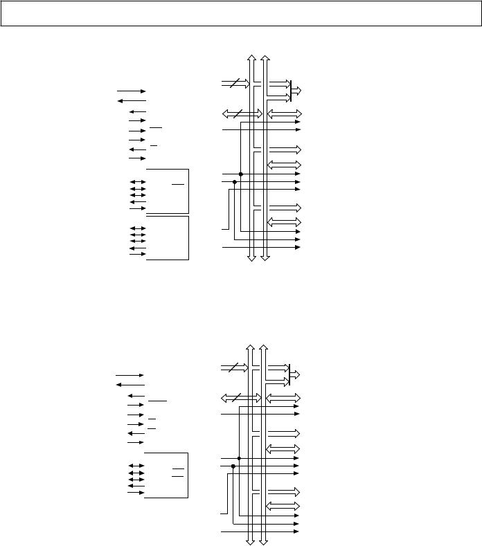
ARCHITECTURE OVERVIEW
Figure 1 shows a block diagram of the ADSP-21xx architecture. The processors contain three independent computational units: the ALU, the multiplier/accumulator (MAC), and the shifter.
The computational units process 16-bit data directly and have provisions to support multiprecision computations. The ALU performs a standard set of arithmetic and logic operations; division primitives are also supported. The MAC performs single-cycle multiply, multiply/add, and multiply/subtract operations. The shifter performs logical and arithmetic shifts, normalization, denormalization, and derive exponent operations. The shifter can be used to efficiently implement numeric format control including multiword floating-point representations.
The internal result (R) bus directly connects the computational units so that the output of any unit may be used as the input of any unit on the next cycle.
A powerful program sequencer and two dedicated data address generators ensure efficient use of these computational units. The sequencer supports conditional jumps, subroutine calls, and returns in a single cycle. With internal loop counters and loop stacks, the ADSP-21xx executes looped code with zero overhead—no explicit jump instructions are required to maintain the loop.
Two data address generators (DAGs) provide addresses for simultaneous dual operand fetches (from data memory and program memory). Each DAG maintains and updates four address pointers. Whenever the pointer is used to access data (indirect addressing), it is post-modified by the value of one of four modify registers. A length value may be associated with each pointer to implement automatic modulo addressing for circular buffers. The circular buffering feature is also used by the serial ports for automatic data transfers to (and from) onchip memory.
Efficient data transfer is achieved with the use of five internal buses:
•Program Memory Address (PMA) Bus
•Program Memory Data (PMD) Bus
•Data Memory Address (DMA) Bus
•Data Memory Data (DMD) Bus
•Result (R) Bus
The two address buses (PMA, DMA) share a single external address bus, allowing memory to be expanded off-chip, and the two data buses (PMD, DMD) share a single external data bus. The BMS, DMS, and PMS signals indicate which memory space is using the external buses.
Program memory can store both instructions and data, permitting the ADSP-21xx to fetch two operands in a single cycle, one from program memory and one from data memory. The processor can fetch an operand from on-chip program memory and the next instruction in the same cycle.
The memory interface supports slow memories and memorymapped peripherals with programmable wait state generation. External devices can gain control of the processor’s buses with the use of the bus request/grant signals (BR, BG).
EZ-ICE and EZ-LAB are registered trademarks of Analog Devices, Inc.
–4– |
REV. B |

|
|
|
|
|
|
|
|
|
ADSP-21xx |
||
|
|
|
|
INSTRUCTION |
PROGRAM |
DATA |
|
|
FLAGS |
|
|
|
|
|
|
REGISTER |
MEMORY |
MEMORY |
|
|
(ADSP-2111 Only) |
3 |
|
DATA |
|
DATA |
|
|
SRAM |
SRAM |
|
BOOT |
|
|
|
|
|
|
|
ADDRESS |
TIMER |
|
|
||||
ADDRESS |
|
ADDRESS |
|
PROGRAM |
or ROM |
|
|
GENERATOR |
|
|
|
GENERATOR |
GENERATOR |
|
|
|
|
|
|
|
|||
|
SEQUENCER |
|
|
|
|
|
|
|
|||
#1 |
|
#2 |
|
|
|
|
|
|
|
|
|
|
|
|
|
|
|
|
|
|
|
||
|
|
14 |
PMA BUS |
|
24 |
|
16 |
PMA BUS |
|
|
|
|
|
|
|
|
|
|
|
|
|
14 |
EXTERNAL |
|
|
14 |
DMA BUS |
|
|
|
|
DMA BUS |
MUX |
|
ADDRESS |
|
|
|
|
|
|
|
|
BUS |
|||
|
|
|
|
|
|
|
|
|
|
|
|
|
24 |
PMD BUS |
|
|
|
|
|
PMD BUS |
|
|
|
|
|
|
|
BUS |
|
|
|
|
24 |
EXTERNAL |
|
|
|
|
|
|
|
|
|
|
|||
|
|
|
|
EXCHANGE |
|
|
|
MUX |
|
DATA |
|
|
16 |
DMD BUS |
|
|
|
|
|
DMD BUS |
|
|
BUS |
INPUT REGS |
INPUT REGS |
INPUT REGS |
|
|
COMPANDING |
HOST |
11 |
||||
|
|
|
|
|
|
|
|
CIRCUITRY |
PORT |
|
|
ALU |
|
|
MAC |
SHIFTER |
TRANSMIT REG |
|
TRANSMIT REG |
CONTROL |
EXTERNAL |
||
|
|
|
|
|
|
|
|
||||
OUTPUT REGS |
OUTPUT REGS |
OUTPUT REGS |
RECEIVE REG |
|
RECEIVE REG |
|
|
HOST PORT |
|||
|
HOST |
16 BUS |
|||||||||
|
|
|
|
16 |
|
SERIAL |
|
SERIAL |
|||
|
|
|
|
|
PORT 0 |
|
PORT |
|
|||
|
|
|
|
|
|
|
PORT 1 |
DATA |
|
||
|
|
|
|
|
(Not on ADSP-2105) |
|
|||||
|
|
|
|
R Bus |
|
|
|
HOST INTERFACE PORT |
|||
|
|
|
|
|
|
5 |
|
5 |
|||
|
|
|
|
|
|
|
(ADSP-2111 Only) |
||||
|
|
|
|
|
|
|
|
|
|||
Figure 1. ADSP-21xx Block Diagram
One bus grant execution mode (GO Mode) allows the ADSP21xx to continue running from internal memory. A second execution mode requires the processor to halt while buses are granted.
Each ADSP-21xx processor can respond to several different interrupts. There can be up to three external interrupts, configured as edgeor level-sensitive. Internal interrupts can be generated by the timer, serial ports, and, on the ADSP-2111, the host interface port. There is also a master RESET signal.
Booting circuitry provides for loading on-chip program memory automatically from byte-wide external memory. After reset, three wait states are automatically generated. This allows, for example, a 60 ns ADSP-2101 to use a 200 ns EPROM as external boot memory. Multiple programs can be selected and loaded from the EPROM with no additional hardware.
The data receive and transmit pins on SPORT1 (Serial Port 1) can be alternatively configured as a general-purpose input flag and output flag. You can use these pins for event signalling to and from an external device. The ADSP-2111 has three additional flag outputs whose states are controlled through software.
A programmable interval timer can generate periodic interrupts. A 16-bit count register (TCOUNT) is decremented every n cycles, where n–1 is a scaling value stored in an 8-bit register (TSCALE). When the value of the count register reaches zero, an interrupt is generated and the count register is reloaded from a 16-bit period register (TPERIOD).
Serial Ports
The ADSP-21xx processors include two synchronous serial ports (“SPORTs”) for serial communications and multiprocessor communication. All of the ADSP-21xx processors have two serial ports (SPORT0, SPORT1) except for the ADSP-2105, which has only SPORT1.
The serial ports provide a complete synchronous serial interface with optional companding in hardware. A wide variety of framed or frameless data transmit and receive modes of operation are available. Each SPORT can generate an internal programmable serial clock or accept an external serial clock.
Each serial port has a 5-pin interface consisting of the following signals:
Signal Name |
Function |
SCLK |
Serial Clock (I/O) |
RFS |
Receive Frame Synchronization (I/O) |
TFS |
Transmit Frame Synchronization (I/O) |
DR |
Serial Data Receive |
DT |
Serial Data Transmit |
The ADSP-21xx serial ports offer the following capabilities:
Bidirectional—Each SPORT has a separate, double-buffered transmit and receive function.
Flexible Clocking—Each SPORT can use an external serial clock or generate its own clock internally.
REV. B |
–5– |

ADSP-21xx
Flexible Framing—The SPORTs have independent framing for the transmit and receive functions; each function can run in a frameless mode or with frame synchronization signals internally generated or externally generated; frame sync signals may be active high or inverted, with either of two pulse widths and timings.
Different Word Lengths—Each SPORT supports serial data word lengths from 3 to 16 bits.
Companding in Hardware—Each SPORT provides optional A-law and μ-law companding according to CCITT recommendation G.711.
Flexible Interrupt Scheme—Receive and transmit functions can generate a unique interrupt upon completion of a data word transfer.
Autobuffering with Single-Cycle Overhead—Each SPORT can automatically receive or transmit the contents of an entire circular data buffer with only one overhead cycle per data word; an interrupt is generated after the transfer of the entire buffer is completed.
Multichannel Capability (SPORT0 Only)—SPORT0 provides a multichannel interface to selectively receive or transmit a 24-word or 32-word, time-division multiplexed serial bit stream; this feature is especially useful for T1 or CEPT interfaces, or as a network communication scheme for multiple processors. (Note that the ADSP-2105 includes only SPORT1, not SPORT0, and thus does not offer multichannel operation.)
Alternate Configuration—SPORT1 can be alternatively configured as two external interrupt inputs (IRQ0, IRQ1) and the Flag In and Flag Out signals (FI, FO).
Host Interface Port (ADSP-2111)
The ADSP-2111 includes a Host Interface Port (HIP), a parallel I/O port that allows easy connection to a host processor. Through the HIP, the ADSP-2111 can be accessed by the host processor as a memory-mapped peripheral. The host interface port can be thought of as an area of dual-ported memory, or mailbox registers, that allows communication between the computational core of the ADSP-2111 and the host computer. The host interface port is completely asynchronous. The host processor can write data into the HIP while the ADSP-2111 is operating at full speed.
Three pins configure the HIP for operation with different types of host processors. The HSIZE pin configures HIP for 8- or 16bit communication with the host processor. HMD0 configures the bus strobes, selecting either separate read and write strobes or a single read/write select and a host data strobe. HMD1 selects either separate address (3-bit) and data (16-bit) buses or a multiplexed 16-bit address/data bus with address latch enable. Tying these pins to appropriate values configures the ADSP2111 for straight-wire interface to a variety of industry-standard microprocessors and microcomputers.
The HIP contains six data registers (HDR5-0) and two status registers (HSR7-6) with an associated HMASK register for masking interrupts from individual HIP data registers. The HIP data registers are memory-mapped in the internal data memory
of the ADSP-2111. The two status registers provide status information to both the ADSP-2111 and the host processor. HSR7 contains a software reset bit which can be set by both the ADSP-2111 and the host.
HIP transfers can be managed using either interrupts or polling. The HIP generates an interrupt whenever an HDR register receives data from a host processor write. It also generates an interrupt when the host processor has performed a successful read of any HDR. The read/write status of the HDRs is also stored in the HSR registers.
The HMASK register bits can be used to mask the generation of read or write interrupts from individual HDR registers. Bits in the IMASK register enable and disable all HIP read interrupts or all HIP write interrupts. So, for example, a write to HDR4 will cause an interrupt only if both the HDR4 Write bit in HMASK and the HIP Write interrupt enable bit in IMASK are set.
The HIP provides a second method of booting the ADSP-2111 in which the host processor loads instructions into the HIP. The ADSP-2111 automatically transfers the data, in this case opcodes, to internal program memory. The BMODE pin determines whether the ADSP-2111 boots from the host processor through the HIP or from external EPROM over the data bus.
Interrupts
The ADSP-21xx’s interrupt controller lets the processor respond to interrupts with a minimum of overhead. Up to three external interrupt input pins, IRQ0, IRQ1, and IRQ2, are provided. IRQ2 is always available as a dedicated pin; IRQ1 and IRQ0 may be alternately configured as part of Serial Port 1. The ADSP-21xx also supports internal interrupts from the timer, the serial ports, and the host interface port (on the ADSP-2111). The interrupts are internally prioritized and individually maskable (except for RESET which is non-maskable). The IRQx input pins can be programmed for either levelor edgesensitivity. The interrupt priorities for each ADSP-21xx processor are shown in Table III.
The ADSP-21xx uses a vectored interrupt scheme: when an interrupt is acknowledged, the processor shifts program control to the interrupt vector address corresponding to the interrupt received. Interrupts can be optionally nested so that a higher priority interrupt can preempt the currently executing interrupt service routine. Each interrupt vector location is four instructions in length so that simple service routines can be coded entirely in this space. Longer service routines require an additional JUMP or CALL instruction.
Individual interrupt requests are logically ANDed with the bits in the IMASK register; the highest-priority unmasked interrupt is then selected.
The interrupt control register, ICNTL, allows the external interrupts to be set as either edgeor level-sensitive. Depending on bit 4 in ICNTL, interrupt service routines can either be nested (with higher priority interrupts taking precedence) or be processed sequentially (with only one interrupt service active at a time).
–6– |
REV. B |

ADSP-21xx
The interrupt force and clear register, IFC, is a write-only register that contains a force bit and a clear bit for each interrupt (except for level-sensitive interrupts and the ADSP-2111 HIP interrupts—these cannot be forced or cleared in software).
When responding to an interrupt, the ASTAT, MSTAT, and IMASK status registers are pushed onto the status stack and the PC counter is loaded with the appropriate vector address. The status stack is seven levels deep (nine levels deep on the ADSP-2111) to allow interrupt nesting. The stack is automatically popped when a return from the interrupt instruction is executed.
Pin Definitions
Table IV (on next page) shows pin definitions for the ADSP21xx processors. Any inputs not used must be tied to VDD.
Table III. Interrupt Vector Addresses & Priority
ADSP-2105 |
|
||||||||
Interrupt |
Interrupt |
||||||||
Source |
Vector Address |
||||||||
|
|
|
|
|
|
|
|
|
|
|
|
Startup |
0x0000 |
||||||
RESET |
|||||||||
IRQ2 |
0x0004 (High Priority) |
||||||||
SPORT1 Transmit or |
IRQ1 |
|
0x0010 |
||||||
SPORT1 Receive or |
IRQ0 |
|
|
0x0014 |
|||||
Timer |
0x0018 (Low Priority) |
||||||||
|
|
|
|
|
|||||
|
|
|
|
|
|||||
ADSP-2101/2103/2115/216x |
|
||||||||
Interrupt |
Interrupt |
||||||||
Source |
Vector Address |
||||||||
|
|
|
|
|
|||||
|
|
Startup |
0x0000 |
||||||
RESET |
|||||||||
IRQ2 |
|
|
|
0x0004 (High Priority) |
|||||
SPORT0 Transmit |
0x0008 |
||||||||
SPORT0 Receive |
0x000C |
||||||||
SPORT1 Transmit or |
IRQ1 |
|
0x0010 |
||||||
SPORT1 Receive or |
IRQ0 |
|
0x0014 |
||||||
Timer |
0x0018 (Low Priority) |
||||||||
|
|
||||||||
|
|
||||||||
ADSP-2111 |
|
||||||||
Interrupt |
Interrupt |
||||||||
Source |
Vector Address |
||||||||
|
|
||||||||
|
Startup |
0x0000 |
|||||||
RESET |
|||||||||
IRQ2 |
0x0004 (High Priority) |
||||||||
HIP Write from Host |
0x0008 |
||||||||
HIP Read to Host |
0x000C |
||||||||
SPORT0 Transmit |
0x0010 |
||||||||
SPORT0 Receive |
0x0014 |
||||||||
SPORT1 Transmit or |
IRQ1 |
|
0x0018 |
||||||
SPORT1 Receive or IRQ0 |
0x001C |
||||||||
Timer |
0x0020 (Low Priority) |
||||||||
|
|
|
|
|
|
|
|
|
|
SYSTEM INTERFACE
Figure 3 shows a typical system for the ADSP-2101, ADSP2115, or ADSP-2103, with two serial I/O devices, a boot EPROM, and optional external program and data memory. A total of 15K words of data memory and 16K words of program memory is addressable for the ADSP-2101 and ADSP-2103. A total of 14.5K words of data memory and 15K words of program memory is addressable for the ADSP-2115.
Figure 4 shows a system diagram for the ADSP-2105, with one serial I/O device, a boot EPROM, and optional external program and data memory. A total of 14.5K words of data memory and 15K words of program memory is addressable for the ADSP-2105.
Figure 5 shows a system diagram for the ADSP-2111, with two serial I/O devices, a host processor, a boot EPROM, and optional external program and data memory. A total of 15K words of data memory and 16K words of program memory is addressable.
Programmable wait-state generation allows the processors to easily interface to slow external memories.
The ADSP-2101, ADSP-2103, ADSP-2115, and ADSP-2111 processors also provide either: one external interrupt (IRQ2) and two serial ports (SPORT0, SPORT1), or three external interrupts (IRQ2, IRQ1, IRQ0) and one serial port (SPORT0).
The ADSP-2105 provides either: one external interrupt (IRQ2) and one serial port (SPORT1), or three external interrupts (IRQ2, IRQ1, IRQ0) with no serial port.
Clock Signals
The ADSP-21xx processors’ CLKIN input may be driven by a crystal or by a TTL-compatible external clock signal. The CLKIN input may not be halted or changed in frequency during operation, nor operated below the specified low frequency limit.
If an external clock is used, it should be a TTL-compatible signal running at the instruction rate. The signal should be connected to the processor’s CLKIN input; in this case, the XTAL input must be left unconnected.
Because the ADSP-21xx processors include an on-chip oscillator circuit, an external crystal may also be used. The crystal should be connected across the CLKIN and XTAL pins, with two capacitors connected as shown in Figure 2. A parallelresonant, fundamental frequency, microprocessor-grade crystal should be used.
CLKIN |
XTAL |
CLKOUT |
ADSP-21xx
Figure 2. External Crystal Connections
REV. B |
–7– |

ADSP-21xx
A clock output signal (CLKOUT) is generated by the processor, synchronized to the processor’s internal cycles.
Reset
The RESET signal initiates a complete reset of the ADSP-21xx. The RESET signal must be asserted when the chip is powered up to assure proper initialization. If the RESET signal is applied during initial power-up, it must be held long enough to allow the processor’s internal clock to stabilize. If RESET is activated at any time after power-up and the input clock frequency does not change, the processor’s internal clock continues and does not require this stabilization time.
The power-up sequence is defined as the total time required for the crystal oscillator circuit to stabilize after a valid VDD is applied to the processor and for the internal phase-locked loop (PLL) to lock onto the specific crystal frequency. A minimum of 2000 tCK cycles will ensure that the PLL has locked (this does not, however, include the crystal oscillator start-up time). During this power-up sequence the RESET signal should be held low. On any subsequent resets, the RESET signal must meet the minimum pulse width specification, tRSP.
To generate the RESET signal, use either an RC circuit with an external Schmidt trigger or a commercially available reset IC. (Do not use only an RC circuit.)
Table IV. ADSP-21xx Pin Definitions
Pin |
# of |
Input / |
|
|
|
|
|
|
|
|||||||||||||||
Name(s) |
Pins |
Output |
Function |
|||||||||||||||||||||
|
|
|
|
|
|
|
|
|
|
|
|
|
|
|
|
|
|
|
|
|
|
|
|
|
Address |
14 |
O |
Address outputs for program, data and boot memory. |
|||||||||||||||||||||
Data1 |
24 |
I/O |
Data I/O pins for program and data memories. Input only for |
|||||||||||||||||||||
|
|
|
|
|
|
|
|
|
|
|
|
|
|
|
|
|
|
boot memory, with two MSBs used for boot memory addresses. |
||||||
|
|
|
|
|
|
|
|
|
|
|
|
|
|
|
|
|
|
Unused data lines may be left floating. |
||||||
RESET |
|
|
|
1 |
I |
Processor Reset Input |
||||||||||||||||||
IRQ2 |
1 |
I |
External Interrupt Request #2 |
|||||||||||||||||||||
BR |
2 |
|
|
|
|
|
|
|
|
|
|
1 |
I |
External Bus Request Input |
||||||||||
BG |
|
|
|
|
|
|
|
|
|
|
|
|
1 |
O |
External Bus Grant Output |
|||||||||
PMS |
|
|
|
|
|
|
|
|
|
|
1 |
O |
External Program Memory Select |
|||||||||||
DMS |
|
|
|
|
|
|
|
1 |
O |
External Data Memory Select |
||||||||||||||
BMS |
|
|
|
|
|
|
|
|
1 |
O |
Boot Memory Select |
|||||||||||||
RD |
1 |
O |
External Memory Read Enable |
|||||||||||||||||||||
WR |
|
|
|
|
|
|
|
|
1 |
O |
External Memory Write Enable |
|||||||||||||
MMAP |
1 |
I |
Memory Map Select Input |
|||||||||||||||||||||
CLKIN, XTAL |
2 |
I |
External Clock or Quartz Crystal Input |
|||||||||||||||||||||
CLKOUT |
1 |
O |
Processor Clock Output |
|||||||||||||||||||||
VDD |
|
|
Power Supply Pins |
|||||||||||||||||||||
GND |
|
|
Ground Pins |
|||||||||||||||||||||
SPORT03 |
5 |
I/O |
Serial Port 0 Pins (TFS0, RFS0, DT0, DR0, SCLK0) |
|||||||||||||||||||||
SPORT1 |
5 |
I/O |
Serial Port 1 Pins (TFS1, RFS1, DT1, DR1, SCLK1) |
|||||||||||||||||||||
or Interrupts & Flags: |
|
|
|
|
|
|
|
|
|
|||||||||||||||
|
IRQ0 |
(RFS1) |
1 |
I |
External Interrupt Request #0 |
|||||||||||||||||||
|
IRQ1 |
(TFS1) |
1 |
I |
External Interrupt Request #1 |
|||||||||||||||||||
|
FI (DR1) |
1 |
I |
Flag Input Pin |
||||||||||||||||||||
|
FO (DT1) |
1 |
O |
Flag Output Pin |
||||||||||||||||||||
FL2–0 (ADSP-2111 Only) |
3 |
O |
General Purpose Flag Output Pins |
|||||||||||||||||||||
Host Interface Port |
|
|
|
|
|
|
|
|
|
|||||||||||||||
(ADSP-2111 Only) |
|
|
|
|
|
|
|
|
|
|||||||||||||||
HSEL |
|
|
|
|
1 |
I |
HIP Select Input |
|||||||||||||||||
HACK |
|
|
1 |
O |
HIP Acknowledge Output |
|||||||||||||||||||
HSIZE |
1 |
I |
8/16-Bit Host Select (0 = 16-Bit, 1 = 8-Bit) |
|||||||||||||||||||||
BMODE |
1 |
I |
Boot Mode Select (0 = Standard EPROM Booting, 1 = HIP Booting) |
|||||||||||||||||||||
HMD0 |
1 |
I |
Bus Strobe Select (0 = |
RD |
/ |
WR |
, 1 = RW/ |
DS |
) |
|||||||||||||||
HMD1 |
1 |
I |
HIP Address/Data Mode Select (0 = Separate, 1 = Multiplexed) |
|||||||||||||||||||||
HRD |
/HRW |
1 |
I |
HIP Read Strobe or Read/Write Select |
||||||||||||||||||||
HWR |
/ |
HDS |
|
1 |
I |
HIP Write Strobe or Host Data Strobe Select |
||||||||||||||||||
HD15–0/HAD15-0 |
16 |
I/O |
HIP Data or HIP Data and Address |
|||||||||||||||||||||
HA2/ALE |
1 |
I |
Host Address 2 Input or Address Latch Enable Input |
|||||||||||||||||||||
HA1–0/Unused |
2 |
I |
Host Address 1 and 0 Inputs |
|||||||||||||||||||||
|
|
|
|
|
|
|
|
|
|
|
|
|
|
|
|
|
|
|
|
|
|
|
|
|
NOTES
1Unused data bus lines may be left floating. 2BR must be tied high (to VDD) if not used.
3ADSP-2105 does not have SPORT0. (SPORT0 pins are No Connects on the ADSP-2105.)
–8– |
REV. B |
ADSP-21xx
|
|
|
|
ADSP-2101 |
|
|
|
|
|
||
|
|
|
|
|
|
|
|
|
|||
|
|
|
|
or |
ADSP-2103 |
|
|
|
|
|
|
|
|
|
|
or |
ADSP-2115 |
14 |
|
A13-0 |
|
|
|
|
|
|
|
|
|
ADDR13-0 |
|
|
BOOT |
||
1x CLOCK |
|
|
CLKIN |
|
|
|
D23-22 |
ADDR |
|||
|
|
|
|
|
|
MEMORY |
|||||
|
or |
|
|
XTAL |
|
|
|
|
|
|
|
CRYSTAL |
|
|
|
|
24 |
|
D15-8 |
|
e.g. EPROM |
||
|
|
|
|
|
|
|
|
|
|||
|
|
|
|
CLKOUT |
DATA23-0 |
|
DATA |
2764 |
|||
|
|
|
|
RESET |
|
|
|
27128 |
|||
|
|
|
|
|
|
|
|
OE |
27256 |
||
|
|
|
|
|
|
|
|
|
|
CS |
|
|
|
|
|
IRQ2 |
|
BMS |
|
|
|
27512 |
|
|
|
|
|
BR |
|
|
|
|
A13-0 |
|
|
|
|
|
|
|
|
|
|
|
|
||
|
|
|
|
BG |
|
|
|
|
ADDR |
|
|
|
|
|
|
|
|
|
|
|
|
||
|
|
|
|
MMAP |
|
|
|
|
D23-0 |
DATA |
PROGRAM |
|
|
|
|
|
|
|
|
|
|
||
|
|
|
|
|
|
|
|
|
|
MEMORY |
|
|
|
|
|
SPORT 1 |
RD |
|
|
|
OE |
||
|
|
|
|
|
|
|
|
||||
|
|
|
|
SCLK1 |
|
WR |
|
|
|
WE |
(OPTIONAL) |
|
SERIAL |
|
RFS1 or IRQ0 |
|
|
|
|
CS |
|||
|
|
|
|
|
|
|
|||||
|
DEVICE |
|
TFS1 or IRQ1 |
|
|
|
A13-0 |
|
|
||
|
|
|
|
|
|||||||
|
(OPTIONAL) |
|
DT1 or |
FO |
|
|
|
|
|
||
|
|
|
ADDR |
DATA |
|||||||
|
|
DR1 or |
FI |
|
|
|
|
||||
|
|
|
|
|
|
|
D23-8 |
||||
|
|
|
|
SPORT 0 |
|
|
|
DATA |
MEMORY |
||
|
|
|
|
|
|
||||||
|
|
|
|
|
|
|
|
& |
|||
|
SERIAL |
|
SCLK0 |
PMS |
|
|
|
OE |
PERIPHERALS |
||
|
|
RFS0 |
|
|
|
|
|
WE |
|
||
|
DEVICE |
|
TFS0 |
|
|
|
|
|
|
||
|
|
|
DMS |
|
|
|
|
(OPTIONAL) |
|||
|
(OPTIONAL) |
|
DT0 |
|
|
|
|
CS |
|||
|
|
DR0 |
|
|
|
|
|
|
|
||
|
|
|
|
|
|
|
|||||
|
|
|
|
|
|
|
|
|
|
|
|
THE TWO MSBs OF THE DATA BUS (D23-22 ) ARE USED TO SUPPLY THE TWO MSBs OF THE
BOOT MEMORY EPROM ADDRESS. THIS IS ONLY REQUIRED FOR THE 27256 AND 27512.
Figure 3. ADSP-2101/ADSP-2103/ADSP-2115 System
|
|
|
|
ADSP-2105 |
|
|
|
|
|
||
|
|
|
|
|
|
A13-0 |
|
|
|||
|
|
|
|
|
|
ADDR13-0 |
14 |
|
|
|
|
|
|
|
|
|
|
|
BOOT |
||||
1x CLOCK |
|
|
CLKIN |
|
|
|
D23-22 |
ADDR |
|||
|
|
|
|
|
|
MEMORY |
|||||
|
or |
|
|
XTAL |
|
|
|
|
|
|
|
CRYSTAL |
|
|
|
|
24 |
|
D15-8 |
|
e.g. EPROM |
||
|
|
|
|
|
|
|
|
|
|||
|
|
|
|
CLKOUT |
DATA23-0 |
|
DATA |
2764 |
|||
|
|
|
|
RESET |
|
|
|
|
27128 |
||
|
|
|
|
|
|
|
|
|
OE |
27256 |
|
|
|
|
|
IRQ2 |
|
|
|
|
|
CS |
|
|
|
|
|
|
BMS |
|
|
|
27512 |
||
|
|
|
|
BR |
|
|
|
|
A13-0 |
|
|
|
|
|
|
|
|
|
|
|
|||
|
|
|
|
BG |
|
|
|
|
ADDR |
|
|
|
|
|
|
|
|
|
|
|
|
||
|
|
|
|
MMAP |
|
|
|
|
D23-0 |
DATA |
PROGRAM |
|
|
|
|
|
|
|
|
|
|
MEMORY |
|
|
|
|
|
SPORT 1 |
RD |
|
|
|
OE |
||
|
|
|
|
|
|
|
|
||||
|
|
|
|
SCLK1 |
|
WR |
|
|
|
WE |
(OPTIONAL) |
|
SERIAL |
|
RFS1 or IRQ0 |
|
|
|
|
CS |
|||
|
|
|
|
|
|
|
|||||
|
DEVICE |
|
TFS1 or |
IRQ1 |
|
|
|
A13-0 |
|
|
|
|
|
|
|
|
|||||||
|
(OPTIONAL) |
|
DT1 or |
FO |
|
|
|
|
|
||
|
|
|
ADDR |
DATA |
|||||||
|
|
DR1 or |
FI |
|
|
|
|
||||
|
|
|
|
|
|
|
D23-8 |
||||
|
|
|
|
|
|
|
|
|
DATA |
MEMORY |
|
|
|
|
|
|
|
|
|
||||
|
|
|
|
|
|
PMS |
|
|
|
& |
|
|
|
|
|
|
|
|
|
|
OE |
PERIPHERALS |
|
|
|
|
|
|
|
|
|
|
|
WE |
|
|
|
|
|
|
|
DMS |
|
|
|
CS |
(OPTIONAL) |
|
|
|
|
|
|
|
|
|
|
|
|
|
|
|
|
|
|
|
|
|
|
|
|
THE TWO MSBs OF THE DATA BUS (D23-22 ) ARE USED TO SUPPLY THE TWO MSBs OF THE
BOOT MEMORY EPROM ADDRESS. THIS IS ONLY REQUIRED FOR THE 27256 AND 27512.
Figure 4. ADSP-2105 System
REV. B |
–9– |
ADSP-21xx
|
|
|
|
ADSP-2111 |
|
|
|
|
A13-0 |
|
|
||
|
|
|
14 |
|
|
|
|
BOOT |
|||||
|
|
|
|
|
|
ADDR13-0 |
|
|
|
|
|||
1x CLOCK |
|
|
CLKIN |
|
|
|
|
|
D23-22 |
ADDR |
MEMORY |
||
|
|
|
|
|
|
|
|
(OPTIONAL) |
|||||
|
or |
|
|
XTAL |
|
|
|
|
|
|
|
|
|
CRYSTAL |
|
|
|
|
24 |
|
|
|
D15-8 |
|
e.g. EPROM |
||
|
|
|
|
|
|
|
|
|
|
|
|||
|
|
|
|
CLKOUT |
DATA23-0 |
|
|
|
DATA |
2764 |
|||
|
|
|
|
|
|
|
|
|
|||||
|
|
|
|
RESET |
|
|
|
|
|
|
27128 |
||
|
|
|
|
|
|
|
|
|
|
|
OE |
27256 |
|
|
|
|
|
IRQ2 |
|
BMS |
|
|
|
|
|
CS |
27512 |
|
|
|
|
BR |
|
|
|
|
|
|
A13-0 |
|
|
|
|
|
|
|
|
|
|
|
|
|
|
||
|
|
|
|
BG |
|
|
|
|
|
|
ADDR |
|
|
|
|
|
|
|
|
|
|
|
|
|
|
||
|
|
|
|
MMAP |
|
|
|
|
|
|
D23-0 |
DATA |
PROGRAM |
|
|
|
|
|
|
|
|
|
|
|
|
||
|
|
|
|
|
|
|
|
|
|
|
|
MEMORY |
|
|
|
|
|
SPORT 1 |
RD |
|
|
|
|
|
OE |
||
|
|
|
|
|
|
|
|
|
|
||||
|
|
|
|
SCLK1 |
|
WR |
|
|
|
|
|
WE |
(OPTIONAL) |
|
SERIAL |
|
RFS1 or IRQ0 |
|
|
|
|
|
|
CS |
|||
|
|
|
|
|
|
|
|
|
|||||
|
DEVICE |
|
TFS1 or |
IRQ1 |
|
|
|
|
|
A13-0 |
|
|
|
|
|
|
|
|
|
|
|||||||
|
(OPTIONAL) |
|
DT1 or |
FO |
|
|
|
|
|
|
|
||
|
|
|
ADDR |
DATA |
|||||||||
|
|
DR1 or |
FI |
|
|
|
|
|
|
||||
|
|
|
|
|
|
|
|
|
D23-8 |
||||
|
|
|
|
SPORT 0 |
|
|
|
|
|
DATA |
MEMORY |
||
|
|
|
|
|
|
||||||||
|
|
|
|
|
|
|
|
|
|
& |
|||
|
SERIAL |
|
SCLK0 |
|
PMS |
|
|
|
|
|
OE |
PERIPHERALS |
|
|
|
RFS0 |
|
|
|
|
|
|
|
WE |
|
||
|
DEVICE |
|
TFS0 |
|
|
|
|
|
|
|
|
||
|
|
|
|
|
|
|
|
|
|
(OPTIONAL) |
|||
|
(OPTIONAL) |
|
DT0 |
|
DMS |
|
|
|
|
|
CS |
||
|
|
DR0 |
|
|
|
|
|
|
|
|
|
||
|
|
|
|
|
|
|
|
|
|||||
|
|
|
|
FL0 |
|
|
|
|
|
|
|
|
|
|
|
|
|
|
|
|
|
|
|
|
|
|
|
|
|
|
|
FL1 |
|
|
|
|
|
|
|
|
|
|
|
|
|
FL2 |
|
|
|
|
|
|
HOST |
|
|
|
|
|
|
HOST INTERFACE PORT |
|
|
PROCESSOR |
|
|
||||
|
|
|
|
7 |
|
|
(OPTIONAL) |
|
|
||||
|
|
|
|
|
|
CONTROL |
|
|
|
|
|||
|
|
|
|
|
|
|
|
|
|
|
|
|
|
|
|
|
|
|
DATA / ADDR |
16 |
|
|
|
|
|
|
|
|
|
|
|
|
|
|
|
|
|
|
|
||
|
|
|
|
|
|
|
|
|
|
|
|
|
|
|
|
|
|
|
|
|
|
|
|
|
|
|
|
THE TWO MSBs OF THE DATA BUS (D23-22 ) ARE USED TO SUPPLY THE TWO MSBs OF THE
BOOT MEMORY EPROM ADDRESS. THIS IS ONLY REQUIRED FOR THE 27256 AND 27512.
Figure 5. ADSP-2111 System
The RESET input resets all internal stack pointers to the empty stack condition, masks all interrupts, and clears the MSTAT register. When RESET is released, the boot loading sequence is performed (provided there is no pending bus request and the chip is configured for booting, with MMAP = 0). The first instruction is then fetched from internal program memory location 0x0000.
Program Memory Interface
The on-chip program memory address bus (PMA) and on-chip program memory data bus (PMD) are multiplexed with the onchip data memory buses (DMA, DMD), creating a single external data bus and a single external address bus. The external data bus is bidirectional and is 24 bits wide to allow instruction fetches from external program memory. Program memory may contain code and data.
The external address bus is 14 bits wide. For the ADSP-2101, ADSP-2103, and ADSP-2111, these lines can directly address up to 16K words, of which 2K are on-chip. For the ADSP-2105 and ADSP-2115, the address lines can directly address up to 15K words, of which 1K is on-chip.
The data lines are bidirectional. The program memory select (PMS) signal indicates accesses to program memory and can be used as a chip select signal. The write (WR) signal indicates a write operation and is used as a write strobe. The read (RD) signal indicates a read operation and is used as a read strobe or output enable signal.
The ADSP-21xx processors write data from their 16-bit registers to 24-bit program memory using the PX register to provide the lower eight bits. When the processor reads 16-bit data from 24-bit program memory to a 16-bit data register, the lower eight bits are placed in the PX register.
The program memory interface can generate 0 to 7 wait states for external memory devices; default is to 7 wait states after
RESET.
Program Memory Maps
Program memory can be mapped in two ways, depending on the state of the MMAP pin. Figure 6 shows the two program memory maps for the ADSP-2101, ADSP-2103, and ADSP-2111. Figure 8 shows the program memory maps for the ADSP-2105 and ADSP-2115. Figures 7 and 9 show the program memory maps for the ADSP-2161/62 and ADSP-2163/ 64, respectively.
–10– |
REV. B |