

Учебники / 0841558_16EA1_federico_milano_power_system_modelling_and_scripting
.pdf
16.4 Over-Excitation Limiter |
373 |
16.3.4Power System Stabilizer Type III
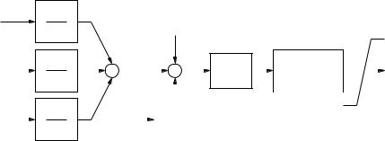
The PSS Type III is depicted in Fig. 16.17, and is described by the equations:
v˙1 = −(KwvSI + v1)/Tw |
|
|
|
|
|
(16.41) |
|||||||||
v˙2 = v3 |
|
|
|
|
|
|
|
|
|
|
|
|
|
|
|
v˙3 = (Kw vSI + v1 − T4v3 − v2)/T2 |
|
|
|
|
|||||||||||
|
|
T1 |
|
T1 |
|
T1 |
|||||||||
vs = v2 + |
|
(KwvSI + v1) + (T3 − |
|
T4)v3 |
+ (1 − |
|
)v2 |
||||||||
T2 |
T2 |
T2 |
|||||||||||||
|
|
|
|
|
|
|
|
|
|
|
|
|
|
vsmax |
|
|
|
|
|
|
|
|
|||||||||
vSI |
Tw s |
|
|
T1s2 + T3s + 1 |
|
|
|
vs |
|||||||
|
Kw |
|
|
|
|
|
|
|
|
|
|
|
|
|
|
|
|
|
|
|
|
T2s2 + T4s + 1 |
|
|
|
|
|
||||
|
Tw s + 1 |
|
|
|
|
|
|
||||||||
|
|
|
|
|
|
|
|
|
|
|
|
|
|
|
|
vsmin
Fig. 16.17 Power system stabilizer Type III control diagram
Example 16.3 E ectiveness of Power System Stabilizers for Removing Hopf Bifurcations
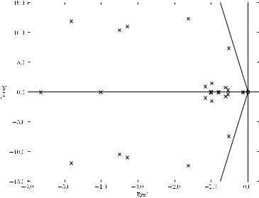
Figure 16.18 shows the eigenvalue loci for the IEEE 14-bus system with a 120% loading level and line 2-4 outage with inclusion of a PSS Type II connected at generator 1. The PSS data are reported in Appendix D. The system is stable and well damped. Thus, in this case, the e ect of the PSS is twofold:
1.To remove the Hopf bifurcation.
2.To properly damp the system (compare Figure 16.18 with the eigenvalue loci of Example 7.1 of Chapter 7).
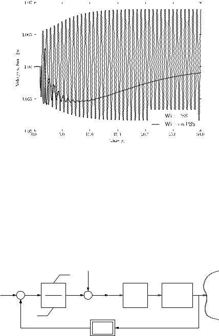
Figure 16.19 compares the transient response of the IEEE 14-bus system with and without PSS at generator 1. As expected from the eigenvalue analysis, the system with PSS is stable and well damped. Furthermore, the PSS allows recovering the generator bus voltage at the desired value. This simulation has to be compared with Figure 16.14 of Example 16.2.
16.4Over-Excitation Limiter
Over-eXcitation Limiters (OXLs) provide an additional signal vOXL to the reference voltage v0ref of AVRs [143]. The OXL is modelled as a pure integrator, with anti-windup hard limits (see Figure 16.20). This regulator is generally sleeping, i.e., vOXL = 0, unless the field current is greater than its
374 |
16 Synchronous Machine Regulators |
|
|
|
|
|
|
|
Fig. 16.18 Eigenvalue loci for the IEEE 14-bus system with 120% loading level, line 2-4 outage and a PSS at generator 1
thermal limit (if > ilimf ≈ 2.7 pu). It is implicitly assumed that at the initial condition given by the power flow solution, all if ≤ ilimf , thus leading to
vOXL = 0 at t = 0. If the field current exceeds its limits the power flow data are not consistent with dynamic ones.
The output signal vOXL is zero as long as if ≤ ilimf . If if > ilimf , the OXL becomes active and undergoes the following di erential equation:
v˙OXL = (if − iflim)/T0 |
(16.42) |
In some cases the direct measure of the field current if is not available. Thus, the field current has to be estimated using available measures. A possible estimation is:
|
|
|
|
|
|
|
γ (v + γ ) + γ2 |
|
|
|
|||
|
|
|
|
− |
|
|
|||||||
|
xq |
|
|
(vh |
+ γq )2 |
+ ph2 |
|
|
|||||
0 = (vh + γq )2 + ph2 + |
|
xd |
+ 1 |
|
q h |
q |
p |
|
if |
(16.43) |
|||
|
|
|
|
|
|
|
|
|
|
|
|
|
|
where
γp = xq ph/vh γq = xq qh/vh
Chapter 17
Direct-Current Devices
This chapter describes dc devices used for modelling hybrid electro-magnetic and electro-mechanical power system models. The devices included in this chapter are: dc nodes (Section 17.1), common interface equations for dc devices (Section 17.2), ideal generators (Section 17.3) and basic components such as RLC circuits (Section 17.4), dc machines (Section 17.5), and unconventional dc generators, namely solid oxide fuel cell, solar photovoltaic cell and energy battery (Section 17.6).
17.1Direct-Current Nodes
Like ac buses, dc nodes has only a topological function. Dc nodes also serve for defining the base dc voltages Vdc,b that are used for computing system pu values of dc devices. Table 17.1 defines all dc node parameters.
Table 17.1 DC node parameters
Variable |
Description |
Unit |
|
|
|
- |
Node code |
- |
v0 |
Initial voltage guess |
pu |
Vdc,n |
Dc voltage rating |
kV |
17.2Common Interface Equations for Direct-Current Devices
Each dc node introduces a new variable (i.e., the node voltage vdc,h) and an equation (i.e., the current balance at that node). The approach used in this section and in the following Chapter 18 for modelling dc devices is the current injection model. As discussed in Chapter 9, the balance equations for the dc system are:
F. Milano: Power System Modelling and Scripting, Power Systems, pp. 379–394. springerlink.com c Springer-Verlag Berlin Heidelberg 2010

380 17 Direct-Current Devices
|
|
|
0 = |
idch,i(x, yˆ, v), h N |
(17.1) |
i Ωh
where idch,i is the current injected at node h by device i and N is the set of nodes of the dc network.
Since all devices described in this section (except for the ground element described in following Section 17.3) connects two nodes, the dc equation interfaces can be standardized in a common class. The general two-node dc device is depicted in Figure 17.1. Using the generator convention, the dc network interface equations are:
0 = vdc,h − vdc,k − vdc(xi, yˆi) |
(17.2) |
|
idc,h |
= idc(xi, yˆi) |
|
idc,k |
= −idc(xi, yˆi) |
|
With this simple interface, completing a device model only requires defining vdc(xi, yˆi) and idc(xi, yˆi) along with one di erential equation per each element of the internal state variables xi and one algebraic equation per each element of the internal algebraic variables yˆi.
+ |
vdc |
− |
vdc,h |
|
vdc,k |
h k
k
idc,h |
idc |
idc,k |
|
Fig. 17.1 General dc device voltages and currents
This approach does not distinguish between series and shunt devices and allows a high grade of flexibility because the same device (i.e., same programming code) can be used both in series and shunt configurations. This is not the case of ac devices described so far. A pure inductive shunt admittance and a pure reactive transmission line are the same electrical element (i.e., a reactance), but require two di erent classes for being defined. The key point is that in the ac network the ground bus is implicitly used by all shunt devices. Hence, the proposed dc device modelling approach requires to explicitly define the ground dc node. The di erent approach used for ac and dc networks has a rationale. For ac networks, defining the ground bus does not provide a significant advantage from the implementation viewpoint since shunt and series devices are conceptually di erent devices with quite di erent functioning. On the other hand, in dc networks, most devices can be connected in series or in parallel (e.g., photovoltaic cell grids).
17.3 Ideal Generators |
381 |
Note on Unit Notation
In this chapter and in the following Chapter 18, the values of dc currents and voltages are considered in pu with respect to the device rated current and voltage, respectively. As discussed in the chapter Notation at the beginning of the book, a dc per-unit system is used for analogy with the ac per-unit system. To maintain consistency, the relative values of resistances, inductances and capacitances are computed as:
R |
|
= |
R(Ω) |
, L |
|
= |
L(H) |
, C |
= C |
R |
|
(17.3) |
(pu) |
|
(s) |
|
dc,n |
||||||||
|
|
|||||||||||
|
|
Rdc,n |
|
|
Rdc,n |
(s) |
(F ) |
|
|
|||
|
|
|
|
|
|
|
|
|
|
|
where the nominal resistance is computed using the nominal power and
voltage device ratings, i.e., Rdc,n = Sn/Vdc,n. In this way, L(s)/R(pu) and C(s)R(pu) are in seconds, as one expects. Whenever absolute values are needed, per-unit quantities are multiplied by the nominal device quantities.
For example, to indicate the power in MW, the notation Snvdcidc will be used.
17.3Ideal Generators
Ideal generators are modelled as assigned functions of the time and can be voltage or current sources. A special case of ideal generator is the ground device, that fixes the voltage reference for a given dc network.
Ideal Independent Sources
Given the interface (17.2), the equation that defines an ideal independent current source is simply:
0 = idc − ides |
(17.4) |
where ides is the current imposed by the generator. In this case, since the current injection is imposed, the equation for the voltage vdc (i.e., the first of (17.2)) is not required.
Analogously, the equation that defines an ideal independent voltage source
is:
0 = vdc − vref |
(17.5) |
where vdes is the voltage imposed by the generator. The current idc is needed as an explicit variable due to the current injection model (17.2).
Ground
The ground works for dc networks similarly to the reference angle in ac ones. Since the ground imposes an absolute value to a node voltage, the interface (17.2) is not required. Similarly to the definition of the reference angle

382 |
17 Direct-Current Devices |
discussed in Section 10.2.2 of Chapter 10, there are at least three possible models, as follows.
1.To assign to the ground node a fixed value, thus removing the voltage at that node from the vector of algebraic variables. This solution reduces the size of the resulting DAE system, but complicates the implementation since it cannot be easily generalized.
2.To leave the ground voltage as a variable, but “freezing” it through setting to zero the row and the column of the Jacobian matrix corresponding to that variable. This method can be easily generalized.
3.To leave the ground voltage as a variable and to include an additional algebraic variable for imposing the desired ground voltage value. This method is very general and do not require manipulating the system Jacobian matrix. Equations are:
idc,h = −iground |
(17.6) |
0 = vdc,h − vground |
|
where iground is a dummy variable and vground is the desired ground voltage. Typically vground = 0.
17.4Basic RLC Models
For the sake of example, this section provide the models of the basic circuit elements depicted in Figure 17.2. The resistance, inductance and capacitance models have to be compared with those based on the Dommel’s method (see Section 8.5 of Chapter 8). The main di erences are that (i) the approach used in this chapter does not depend on the integration step length and (ii) does not require any hypothesis about the linearity of the devices. Table 17.2 summarizes the parameters required for basic RLC elements.
Table 17.2 RLC parameters
Variable Description Unit
R |
Resistance |
pu |
L |
Inductance |
s |
C |
Capacitance |
s |
• Resistance (Figure 17.2.a):
0 = vdc/R + idc |
(17.7) |