

Учебники / 0841558_16EA1_federico_milano_power_system_modelling_and_scripting
.pdf17.6 Other Direct-Current Devices |
393 |
and the SOC is defined as: |
|
|
|
|
|
|
SOC = |
Qn − Qe |
= 1 |
− |
q |
e |
(17.34) |
|
Qn |
|
|
|||
where Qe is the extracted capacity in Ah and remaining parameters are defined in Table 17.6. Figure 17.7 shows a typical discharge of a battery.
Fig. 17.7 Battery discharge characteristic
In the literature, several other battery models have been proposed. For example, the so-called universal model [320] and a Thevenin’s equivalent model including resistive and capacitive elements [264]. While the universal model is basically a linearization of the previous model (17.32), the Thevenin’s battery equivalent attempts to model the battery capacity through fictitious capacitors. The latter model can be linear (constant parameters) or nonlinear (the parameters depend on the SOC).
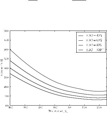
Apart from the SOC, another aspect that has to be taken into account in battery models is the parameter dependence on the temperature. In particular, the internal and polarization resistances are a function of the average battery temperature Θ. Figure 17.8 shows some typical empirical curves of the battery equivalent total internal resistance as a function of both Θ and SOC [235]. As a consequence of the internal resistance is that, during the charge and discharge processes, the battery generates heat proportionally to the energy transit in the time interval. To avoid over-heating, the battery has to be cooled down. The battery temperature dynamic can be written as:
394 |
17 Direct-Current Devices |
Θ˙ = |
1 |
Ed |
|
cpmg Snvdcidc(1 − ηv + |
Vdc,nvoc ) |
(17.35) |
|
|
−hcAc(Θ − Θa) − σεAr (Θ4 − Θa4) |
|
|
where σ = 5.670 · 10−8 W/m2/K4 is the Stefan-Boltzmann’s constant. |
|||
Fig. 17.8 Battery internal resistance as a function of temperature and state of charge
Table 17.6 Energy battery parameters
Variable |
Description |
Unit |
|
|
|
Ac |
Cell e ective convection area |
m2 |
Ar |
Cell e ective radiation area |
m2 |
cp |
Average battery specific heat |
J/kg/K |
Ed |
Average power loss per ampere of discharge |
W/A |
hc |
Convection-cooling coe cient |
W/K/m2 |
Kp |
Polarization constant |
pu/pu |
mg |
Battery mass |
kg |
Qn |
Rated battery capacity |
Ah |
Ri |
Internal battery resistance |
Ω |
Rp |
Polarization resistance |
pu |
voc |
Open circuit potential |
pu |
ve |
Exponential voltage |
pu |
βe |
Exponential capacity coe cient |
1/pu |
ε |
Emittance |
- |
ηv |
Voltage e ciency factor on discharge |
- |
Θa |
Ambient temperature |
K |
396 |
18 AC/DC Devices |
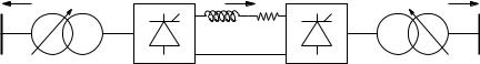
e.g., Ferranti’s e ect and delays (see Section 11.1 of Chapter 11). HVDC are also the unique choice in case of long submarine connections. Another interesting application is in the back-to-back configuration, which consists in connecting the rectifier and the inverter dc sides without the dc line. The back-to-back configuration is useful to decouple system frequencies. For example a back-to-back HVDC device is necessary to interconnect two ac systems working at di erent nominal frequencies (e.g., Japanese interconnected system) or if one of the ac sides shows a poor frequency regulation and the other side wants to avoid problems. Finally, a configuration that includes a rectifier and a dc load are used in some industrial applications (e.g., arc furnaces).
The most flexible manner to implement a general HVDC system is to divide the system into its minimal entities:
1.Ac/dc converter (rectifier and inverter).
2.Dc network.
3.Regulators.
In this way, any HVDC configuration (including multi-terminal ones) and control can be implemented with the minimum e ort. Dc network elements are described in Chapter 17. Following subsections present the models of converters and HVDC controllers used for a standard two-terminal connection. The interested reader can find a discussion on multi-converter HVDC systems in [16].
18.1.1Per Unit System for DC Quantities
In [163], the following bases are used for computing the dc per unit quantities:
|
|
√ |
|
|
|
|
V dc |
= |
3 |
2 |
V ac |
(18.1) |
|
|
|
|||||
base |
|
π |
base |
|
||
|
|
|
|
|||
Idc |
= Idc |
= Idc |
|
|||
base |
|
rate |
n |
|
||
Sdc |
= V dc |
Idc |
|
|||
base |
|
base |
base |
|
||
Zdc |
= V dc |
/Idc |
|
|||
base |
|
base |
base |
|
||
Furthermore, Sn ≈ VndcIndc holds to avoid inconsistencies. In the following subsections, the dc power base is assumed equal to the ac one, i.e., Sbasedc = Sn.
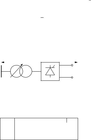
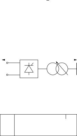
18.1.2Rectifier Model
The rectifier scheme with current and voltage sign notation is shown in Figure 18.2. The dc-side interface equations are (17.2), i.e., the same as any two-terminal dc device described in Chapter 17. According to the notation of Figure 18.2, the active and reactive power injections at the ac-side are:
18.1 High-Voltage Direct-Current Transmission System |
399 |
A common control scheme for the HVDC transmission system scheme of Figure 18.1 is as follows.
Rectifier current control mode (RCCM): Rectifier-side regulators control the dc current idc through a PI controller that varies the firing angle α, and the ac voltage vh through the o -nominal tap ratio mR. Inverter-side regulators maintain constant the extinction angle γ = γref ≥ γmin and control the dc voltage vI,dc through the tap ratio mI . The DAE system is as follows:
x˙ R,m |
= (vh − vacref )/TR |
(18.5) |
x˙ I,m |
= (vdcref − vI,dc)/TI |
|
0 = mR − xR,m |
|
|
0 = mI − xI,m |
|
|
x˙ R,i |
= Ki(idcref − idc) |
|
0= xR,i + Kp(irefdc − idc) − α
0= γref − γ
The PI control undergoes an anti-windup limiter (see Section C.2 of Appendix C) to maintain the firing angle within its limits. The state variable xR,m and xI,m are introduced to allow a general interface with the converter and rectifier models.
Inverter current control mode (ICCM): Inverter-side regulators control the dc current idc through the extinction angle γ and the the ac voltage vk through the tap ratio mI . Rectifier-side regulators maintain constant the firing angle α = αmin and control the dc voltage vR,dc through the tap ratio mR. The DAE system is as follows:
x˙ R,m |
= (vdcref − vR,dc)/TR |
(18.6) |
x˙ I,m |
= (vk − vacref )/TI |
|
0 |
= mR − xR,m |
|
0 |
= mI − xI,m |
|
0 |
= αmin − α |
|
x˙ I,i |
= Ki(idcref + idc − idcm ) |
|
0 |
= xI,i + Kp(idcref + idc − idcm ) − γ |
|
where the current margin imdc avoids that the RCCM and ICCM controls overlap. As for the RCCM, the state variables undergo anti-windup limiters.
Power control : If a power/frequency control is required, the reference current irefdc can be the output of a power (or master ) control, as follows [184]:
idcref = min{idcdes, idclim} |
(18.7) |
400 |
|
18 |
AC/DC Devices |
vdc |
|
Normal |
|
|
|
|
|
|
Rectifier |
Operating Point |
|
kmRvh cos αmin |
|
|
|
|
α = αmin |
|
|
kmI vk cos(π − γref ) |
|
γ = γref |
|
|
|
Inverter |
|
|
idcm |
|
|
0 |
|
|
|
0 |
idcref |
idc |
|
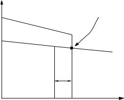
Fig. 18.4 HVDC steady state characteristic for the rectifier current control mode
where idesdc = pref /vdc is the current that provides the desired reference power pref and vdc is the dc voltage at one of the two converter terminals, and ilimdc is defined based on the dc voltage value, as follows:
|
|
imin, if vdc < vmin |
|
|
|
|
|
|
|||||
|
i |
dc |
+ c(v |
|
|
dc |
|
|
|
|
|
|
|
|
|
|
|
v ), if v > v |
|
|
|
||||||
idclim = |
idcmin |
+ c(vdc |
|
vdcmin), |
if vdcmin |
≤ |
vdc |
vdcmax |
(18.8) |
||||
|
min |
|
max− |
min |
|
|
max≤ |
|
|
||||
|
|
|
|
|
|
− dc |
|
|
|
|
|
|
|
|
dc |
|
dc |
dc |
|
|
dc |
|
|
||||
where, typically, c = 1 pu/pu.
Figure 18.4 summarizes the steady-state characteristic of the HVDC control for the RCCM, whereas Table 18.3 summarizes and defines the parameters of the HVDC controllers.
18.2Voltage Source Converter
The Voltage Source Converter (VSC) device is similar to the rectifier or inverter devices of the HVDC transmission system. Thus, the VSC provides a link between an ac and and dc networks. The main di erence with HVDC systems is the technology of power electronic switches. HVDC devices are built using conventional thyristors, which provide the turn-on control, but can be turned o only if the current is zero. The electronic switches used for VSC devices are Gate Turn-O Thyristor (GTO), MOS Turn-o Thyristor (MTO), Integrated Gate Bipolar Transistor (IGBT) or Integrated Gate-Commutated Thyristor (IGCT). These are called turn-o devices since they provide both turn-on and turn-o controls, the latter also for non-zero currents. Turn-o devices are more expensive and have higher losses than conventional thyristors. These drawbacks implies that the typical VSC capacity is smaller than
18.2 Voltage Source Converter |
401 |
|||
|
|
Table 18.3 HVDC control parameters |
|
|
|
|
|
|
|
|
Parameter |
Description |
Units |
|
|
|
|
|
|
|
c |
Slope of the voltage/current power control |
pu |
|
|
idcm |
Current margin |
pu |
|
|
idcmin |
Minimum dc current |
pu |
|
|
Ki |
Integral gain for the current PI control |
1/s |
|
|
Kp |
Proportional gain for the current PI control |
rad/pu |
|
|
pref |
Power reference |
pu |
|
|
TI |
Inverter control time constant |
s |
|
|
TR |
Rectifier control time constant |
s |
|
|
vmax |
Maximum dc voltage |
pu |
|
|
dc |
|
|
|
|
vmin |
Minimum dc voltage |
pu |
|
|
dc |
|
|
|
|
vdcref |
Reference dc voltage |
pu |
|
|
vacref |
Reference ac voltage |
pu |
|
|
αref |
Reference firing angle |
rad |
|
|
γref |
Reference extinction angle |
rad |
|
HVDC ones. However, the turn-o ability allows obtaining controls with higher flexibility than those that can be implemented for HVDC systems. In practice, VSC are used for small to medium power applications such as FACTS devices, wind turbines and other distributed energy resources.
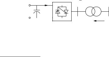
The VSC scheme is shown in Figure 18.5. The typical configuration includes a capacitor, a bi-directional inverter and a transformer. The capacitor allows maintaining constant the dc voltage while the transformer provides a Galvanic insulation. The ac/dc conversion is provided by the VSC, which also includes a series phase reactor and a shunt ac filter.1 The dc voltage is converted into an ac one whose magnitude depends on the VSC modulating amplitude am and whose phase is the inverter firing angle α.
idc |
83 amvdc α |
vac θac |
|
+
vdc
−
pac + jqac , iac φac
VSC
Fig. 18.5 Voltage source converter scheme
The dc-side interface is defined by (17.2). In principle, the elements connected to the dc terminals of the VSC are not part of the VSC model. However, in most cases, the dc side of the VSC contains at least a capacitor used
1The phase reactor and the shunt ac filter as well as the phase-locked loop are not modelled in this chapter since their e ects are relevant only for electromagnetic transients.
402 |
18 AC/DC Devices |
for fixing the dc voltage (see Figure 18.5). The capacitor can be modelled as a parallel RC described by equations (17.10) provided in Chapter 17. To work properly, the dc network must contain two nodes, one of which is connected to the ground. The VSC and the RC element are connected in parallel to the dc nodes. From the implementation viewpoint, it is better that the capacitor is independent from the VSC model. This allows more flexibility in the configuration of the dc side (see for example the di erent configurations described in [129]). On the other hand, the ac/ac transformer can be embedded in the VSC model. The ac-side interface is:
pac = gT vac2 − 3/8 amvdcvacgT cos(θac − α) (18.9)
−3/8 amvdcvacbT sin(θac − α)
qac = −bT vac2 + 3/8 amvdcvacbT cos(θac − α)
−3/8 amvdcvacgT sin(θac − α)
where gT + jbT = 1/(rT + jxT ) is the transformer series admittance. The power balance between the dc and the ac sides is:
0 = gT ( 3/8 amvdc)2 − 3/8 amvdcvacgT cos(θac − α) (18.10)
+3/8 amvdcvacbT sin(θac − α)
Finally, it is important to monitor the ac current to avoid overloading VSC circuits. The ac current iac φac can be obtained imposing the following constraints:
0 |
= pac2 + qac2 − vaciac |
(18.11) |
0 |
= pac sin(θac − φac) − qac cos(θac − φac) |
|
The VSC parameters are defined in Table 18.4 according to the implementation choice of maintaining the capacitor as an independent device.
Table 18.4 Voltage source converter parameters
Variable |
Description |
Unit |
|
|
|
iacmax |
Maximum ac current |
pu |
idcmax |
Maximum dc current |
pu |
ammax |
Maximum modulating amplitude |
pu |
ammin |
Minimum modulating amplitude |
pu |
rT |
Transformer resistance |
pu |
xT |
Transformer reactance |
pu |
αmax |
Maximum firing angle |
rad |
αmin |
Minimum firing angle |
rad |