

Vankka J. - Digital Synthesizers and Transmitters for Software Radio (2000)(en)
.pdfSources of Noise and Spurs in DDS |
|
101 |
|||
|
A(0 |
L M , N) |
2 ªsin 2 (π / N) |
(π / MN) 2 |
º |
|
|||||
|
|
|
(7.18) |
||
|
|
|
¬ (π / N) 2 |
sin 2 (π / MN) ¼ |
|
|
|
|
|||
There are three interesting properties of |
A(0, L M N) |
2 worth mention- |
|||
ing: |
|
|
|
|
|
1)For M = 1, A(0, L, 1, N) 2 = 1, hence there is no spurious harmonic component due to the phase truncation.
2) For a fixed N «A(0, L, M N) 2 is a decreasing function of M. Therefore,
the S/N is also decreasing on M
3)For a fixed M A(0, L M N) 2 is an increasing function of N. Hence, the S/N can be made arbitrarily large by choosing a sufficiently large N
From the properties listed above, we can have closed-form expressions for both the maximum and the minimum S/N for a fixed N, by making M = 2
and , respectively, as follows: |
|
|
|
[ |
|
|
|
|
|
|
|
|
|
|
|
|
|
|
|
|
] |
|
|
|
|
|
|
|||
S / N (max) 20 log10 |
|
|
|
|
|
|
π |
|
|
|
|
|
|
|
|
|
|
|
|
(7.19) |
||||||||||
|
|
|
|
|
|
|
|
|
|
|
|
|
|
|
|
|
||||||||||||||
|
|
|
|
|
|
|
|
|
|
|
|
|
|
|
|
|
|
|
|
|
|
|||||||||
and |
|
|
|
|
|
|
|
|
|
|
|
|
|
|
|
|
|
|
|
|
|
|
|
|
|
|
|
|
||
ª |
|
[ |
|
|
π |
|
|
|
|
|
|
π |
|
|
|
|
]2 |
º |
||||||||||||
|
|
|
|
|
|
|
|
|
|
|
|
|
|
|
|
|||||||||||||||
S / N (min) 10 log10 |
|
|
|
|
|
|
|
|
|
|
|
|
|
|
|
|
|
|
|
|
|
|
|
|
|
|
|
(7.20) |
||
|
[ |
|
|
|
π |
|
|
|
|
|
|
|
|
|
|
π |
|
|
|
|
]2 |
|||||||||
|
¬1 |
|
|
|
|
|
|
|
|
|
|
|
|
|
|
|
¼ |
|
||||||||||||
|
|
|
|
|
|
|
|
|
|
|
|
|
|
|
|
|
|
|
|
|||||||||||
For a reasonably large N, say N > 10 (in practice, N is larger than 1000), (7.19) and (7.20) can be simplified by expanding the arguments of the log function in (7.19) and (7.20) in the Taylor’s series form, and retaining only
the first significant term. By doing so, we obtain |
|
(ʌ/ 2) |
||
S / N (max) |
20log10 (N) |
10 log10 |
||
|
6 02 k − 3 92 dB, |
|
(7.21) |
|
|
|
|
||
and |
|
|
|
|
S / N (min) |
20 log10 (N) |
10 log10 |
(π 2 / 3) |
|
|
6 02 k 5 17 dB. |
|
(7.22) |
|
|
|
|
||
|
|
|
|
|
Equations (7.21) and (7.22) give very handy and accurate estimates of the S/N as a function of the size of the sine LUT [Jen88b].
The SP is defined as the ratio of the power of the desirable harmonic component to the power of the spurious harmonic components
|
ª A(0 L M N) 2 |
º |
||||
SP(r) 10 log10 |
2 |
(7.23) |
||||
|
|
¬ A(r L M , N) |
¼ |
|
|
|
|
|
|
||||
102 |
|
|
|
|
|
|
|
|
|
|
|
|
|
|
|
|
|
Chapter 7 |
where A(0, L M N) 2 and A( |
L M N) 2 |
can be readily obtained from |
||||||||||||||||
(7.15) |
|
|
|
|
|
|
|
|
|
|
|
|
|
|
|
|
N M )) 2 |
|
|
|
|
|
|
|
|
sinc(1 / N ) |
|
|
|
|
|
|
|
|
|
||
SP |
|
r) |
|
|
|
|
|
|
sinc(N r / (N M ) |
|
|
1 / ( |
|
|||||
( |
|
10log |
|
( |
|
|
|
|
|
|
|
|
|
|
|
) |
||
|
|
|
|
|
|
|
|
|
|
|
|
|
||||||
|
|
|
|
|
|
|
sinc(1 / |
(N M )) |
|
r |
|
|
|
/ N ) 2 |
(7.24) |
|||
r 
 ,...,M
where sinc(x) = sin(πx)/πx
The corresponding spur locations for quadrature DDS (complex in-input to Discrete Fourier Transform (DFT)) are given by


 ), (7.25)
where = 1,…M-1 and 0 ≤ F( ) ≤ Pe-1, the DFT size is NM, which is equal to the period of the DDS output (Pe) from (4.4). If the location of a spur were calculated using (7.25), and if the resulting spur number, F( ), was larger than Pe/2, then the aliased positions of the spurs for cosine DDS output (real input to the DFT) are
|
|
|
), |
(7.26) |
|
|
|
||
|
|
|
|
|
where 0 ≤ F( ) ≤ Pe/2. The worst case signal to spur power ratio (minimum ratio) occurs when = M-1 in (7.24) [Jen88a]. The signal to spur power ratios from minimum to maximum are in the following order SP(M-1), SP(1),
SP(M-2), SP(2), SP(M-3)… in (7.24). The worst-case carrier to the spur ratio due to the phase truncation occurs when M = 2 ( = 1)
SP(1) |
ª A(0, , 2, |
) 2 º |
20 log |
♠ |
π |
≡ |
(7.27) |
10 log10 |
) 2 ¼ |
cot( |
|
) . |
|||
|
¬ A(1, , 2, |
|
¬ |
2 N ¼ |
|
||
The carrier to spur ratio due to the phase truncation when |
= 1 and M |
|||||||||||||||||||
(2j k >> GCD(∆P, 2j-k) in (7.7) is given by |
|
|
|
|
|
|
|
|
|
|
|
|
||||||||
|
|
|
|
ª A(0, |
|
|
|
|
) º |
|
|
|
|
|
|
|
|
|
||
SP(1) |
|
|
|
, |
|
, |
|
|
[ |
|
|
|
|
|
]. |
|
||||
|
|
|
20 log 10 |
|
|
|
|
|
|
20 log |
|
|
|
|
|
1 |
(7.28) |
|||
|
|
|
|
|
|
|
|
|
|
|
|
|||||||||
|
|
|
|
|
|
|||||||||||||||
|
|
|
|
¬ A(1, |
, |
|
, |
) ¼ |
|
|
|
|
|
|
|
|
|
|||
|
|
|
|
|
|
|
|
|
|
|
|
|
|
|
|
|||||
For a reasonably large N say N > 10 (in practice, N is larger than 1000),
(7.27) can be simplified by expanding the argument of the log function in (7.27) in the Taylor’s series form and retaining only the first significant term. By doing so, we obtain the worst-case carrier to spur ratio
SP(1) |
|
|
|
20 log |
|
( |
|
) |
|
20 log 10 |
ªπ º |
6.02 |
|
|
|
3.92 dB. |
(7.29) |
||
|
|
|
|
|
|
|
|
|
|||||||||||
|
|
|
|
|
|
||||||||||||||
|
|
|
|
|
|
|
¬ 2 ¼ |
|
|
|
|
||||||||
|
|
|
|
|
|
|
|
|
|
|
|
|
|
|
|
|
|
|
|
The carrier to spur ratio due to the phase truncation when |
= 1 and M |
||||||||||
(from (7.28) is |
|
|
|
|
|
|
|
|
|
|
|
SP(1) |
|
|
|
20 log |
|
( |
|
|
|
. |
(7.30) |
|
|
) |
|
6.02 |
|||||||
|
|
|
|
|
|||||||
The phase truncation error analysis in [Jen88b] is extended here so that it includes the worst-case carrier to spur ratio bounds (7.29) and (7.30). The

Sources of Noise and Spurs in DDS |
103 |
spur power is concentrated in one peak in Figure 8-2, because M is 2 (7.8). The worst-case carrier-to-spur level due to the phase truncation appears to be 44.24 dBc. The expect worst-case carrier-to-spur value is 44.17 dBc (7.29), which agrees closely. The frequency bin of the worst case spur in Figure 8-2 is 1784 (8 F(1)), where F(1) is from (7.25) and (7.26) and the DFT is calculated over eight DDS output periods (Pe). If M is larger than 2, the spur power is spread over many peaks (see Figure 8-3). The number of spurs is 15 from (7.8) in Figure 8-3 Since M = 16 for this case, the expected worst-case carrier-to-spur value is approximately 48.16 dBc (7.30). The worst-case car- rier-to-spur level due to the phase truncation appears to be 48.08 dBc.
7.2 Finite Precision of Sine Samples Stored in LUT
Finite quantization in the sine LUT values also leads to the DDS output spectrum impairments. If it is assumed that the phase truncation does not exist, then the output of the DDS is given by
sin( |
2π |
(∆P n)) eA (n), |
(7.31) |
|
2 j |
||||
|
|
|
where eA(n) is the quantization error due to the finite sine LUT data word. The sequence of the LUT quantization errors is periodic, repeating every Pe samples (4.4). There are two limiting cases, i.e. cases where the numerical period of the output sequence (Pe) is either long or short, to consider.
In the first case, the quantization error results in what appears to be a white noise floor, but is actually a "sea" of very finely spaced discrete spurs. The amplitude quantization errors can be assumed to be totally uncorrelated
and uniformly distributed within each quantization step, |
|
||||
∆ A ≤ e |
A |
≤ ∆ A |
(7.32) |
||
2 |
2 |
|
|||
|
|
|
|||
where the quantization step size is |
|
|
|
|
|
∆ A |
|
|
1 |
|
(7.33) |
|
|
|
|
||
|
2m |
||||
|
|
|
|||
and where m is the word length of the sine values stored in the sine LUT. Then the amplitude error power is [Ben48]
|
|
|
|
∆ A |
|
|
|
|
|
2 |
|
1 |
|
2 |
2 |
|
|
∆2A |
|
E{eA |
} |
∆ |
A |
³ |
eA |
deA |
= |
12 |
(7.34) |
|
|
|
∆ A |
|
|
|
|
|
|
|
|
|
|
2 |
|
|
|
|
|
The signal power of the sine wave is

104 |
Chapter 7 |
A2
PA (7.35)
2
where A is the amplitude of the sine wave. In the DDS literature, there is well-known formula for the signal to noise ratio due to the amplitude quantization (rounding)
|
|
§ S · |
|
|
|
§ |
P |
· |
|
|
§ |
P |
· |
|
|
|
|
) dB, (7.36) |
|||
|
|
|
10 log |
10 |
|
|
A |
|
10 log 10 |
|
|
|
|
CA |
|
≈ (1.76 |
|
6.02 |
|
||
|
|
|
|
|
|
|
|
|
|
|
|
||||||||||
© N ¹ |
© |
E { |
|
} ¹ |
|
|
© |
E { |
|
} ¹ |
|
|
|||||||||
|
|
|
|
|
|
|
|
|
|
|
|||||||||||
|
|
|
|
|
|||||||||||||||||
where PA is A2/2 (sine wave power), PCA is A2 (quadrature wave power), A is 0.5 in (7.36) and the quantization power of the sine wave
E { |
|
|
|
} |
∆2 |
2 2 |
(7.37) |
||
|
|
||||||||
|
|
|
|
|
|
|
12 |
12 |
|
and the error power for the quadrature output signal is |
|
||||||||
E { |
|
|
} |
∆2 |
2 2 |
(7.38) |
|||
|
|
|
|
||||||
|
|
|
|
|
|
|
6 |
6 |
|
where ∆ is the phase to amplitude converter step size and |
is the phase to |
||||||||
amplitude converter wordlength. |
|
|
|
||||||
Comparing (7.22) and (7.36), if k ≤ + 2, then the phase truncation dominates S/N, otherwise amplitude quantization. Due to the sine/cosine wave symmetry the error is also symmetric, therefore the spurs located at the even bin positions are zero for all phase increment words [Tie71] (Pe/2 spurs for cosine output and Pe/4 spurs for quadrature output, where the period of the DDS output (Pe) is from (4.4)). The cosine generated is real, so its power is equally divided into negative and positive frequency components. The quadrature output is complex, so its power is in one frequency component. Therefore, the amplitude quantization noise floor is from (7.36) for the cosine output and quadrature output
NF ≈ (1.76 |
6.02 |
|
|
10 log10 |
|
§ |
Pe |
· |
|
) dBc, when Pe 1. |
(7.39) |
|
|
||||||||||
|
|
|
|
||||||||
|
|
|
|||||||||
|
|
|
© |
4 ¹ |
|||||||
|
|
|
|
|
|
|
|||||
In the second case, there will be no quantization errors if the samples match exactly the quantization levels, e. g., f ut f
ut f /4. The assumption that the error is evenly distributed in one period is really not valid due to the shortness of the period. Assuming that the amplitude error gets its maximum absolute value (∆A/2) at every sampling instance, and that all the energy is in one spur, the carrier-to-spur ratio is
|
§ C · |
|
|
|
|
|
§ |
4 P |
· |
|
|
|
|
|
|
(7.40) |
|
|
|
= 10 |
|
log10 |
|
|
|
A |
= ( |
3.01 |
6.02 |
|
) dBc. |
||||
© S ¹ |
|
|
|
© |
∆2A |
¹ |
|
|
|||||||||
|
|
|
|
|
|
|
|
|
|
|
|||||||
|
|
|
|
|
|
|
|
|
|||||||||
|
|
|
|
|
|
|
|
|
|||||||||
However, simulations indicate that in the worst-case the sum of the discrete spurs is approximately equal to
Sources of Noise and Spurs in DDS |
105 |
||||||
|
∆P = 1 |
∆P = 3 |
|||||
P(0) |
0 |
|
|
|
|
0 |
GCD(1,2j) = GCD(3,8) = 1 |
|
|
|
|
||||
P(1) |
1 |
|
3 |
|
|||
P(2) |
2 |
|
|
|
|
6 |
|
|
|
|
|
|
|||
P(3) |
3 |
|
|
|
1 |
|
|
|
|
|
|
||||
P(4) |
4 |
|
|
4 |
|
||
|
|
|
|||||
P(5) |
5 |
|
|
7 |
|
||
|
|
|
|||||
P(6) |
6 |
|
|
2 |
|
||
|
|
|
|||||
P(7) |
7 |
|
|
5 |
|
||
|
|
|
|||||
Figure 7-3. Time series vectors for a 3-bit phase accumulator for ∆P = 1 and ∆P = 3. The column vector for ∆P = 3 can be formed from a permutation of the values of the ∆P = 1 vector, regardless of the initial phase accumulator contents.
|
§ C · |
|
§ P |
· |
|
|
|
|
|
|
A |
|
|
(1 76 + 6 02 m) dBc |
(7.41) |
|
© Ssum ¹ |
|
© E{eA2 |
} ¹ |
|
||
|
|
|
|
||||
|
|
|
|||||
7.3 Distribution of Spurs
One of the advantages of a DDS is its ability to provide a continuous phase when changing phase increment words; the phase accumulator need not be reset when a new ∆P is applied. The state of the phase accumulator at the point in time when a new ∆P is applied provides a natural phase-offset for the subsequent DDS output, thereby providing continuous-phase frequency switching. The initial phase of the phase accumulator at the time when a new ∆P is applied could, however, also be a factor in determining the output spurs.
The j-bit phase accumulator can be considered as a permutation generator, where each value of ∆P provides a different permutation of the values from 0 to 2j - 1 given by
∆P = 2 |
∆P = 6 |
|||||||||
P(0) |
0 |
|
|
|
|
|
|
0 |
GCD(2,2j) = GCD(6,8) = 2 |
|
|
|
|
|
|
|
|||||
P(1) |
2 |
|
6 |
|
||||||
P(2) |
4 |
|
|
|
|
|
|
4 |
|
|
|
|
|
|
|
||||||
P(3 |
6 |
|
|
|
|
2 |
|
|||
|
|
|
|
|||||||
∆P = 2 |
∆P = 6 |
|||||||||
P(0) |
1 |
|
1 |
|
||||||
P(1) |
3 |
|
7 |
|
||||||
P(2) |
5 |
|
|
|
5 |
|
||||
|
|
|
||||||||
P(3) |
7 |
|
|
|
3 |
|
||||
|
|
|
||||||||
Figure 7.4. Time series vectors for a 3-bit accumulator for ∆P = 2 and ∆P = 6.

106 |
|
|
|
|
|
|
|
|
Chapter 7 |
ǻP |
P( |
|
) ( |
|
|
ǻP |
p |
)mod 2 j |
(7.42) |
|
|
|
|
|
The output vector generated by the phase accumulator depends on the phase increment word and on the initial accumulator value, i.e., the initial phase (p) in (7.42). In Figure 7-3, any phase accumulator output vector can be formed from the permutation of another output vector, regardless of the initial phase accumulator contents, when GCD(∆P, 2j) = 1 for all values of ∆P. In Figure 7.4, the time vectors are formed from phase increment values that have the property GCD(∆P, 2j) = 21 when the initial phase is not same (0 and 1). From this figure it is evident that the phase accumulator is now characterized by having two different sets of possible output vectors, depending on the initial contents of the phase accumulator.
The number of the least significant bits (i), which are zero in the phase increment word, can be obtained from
|
|
|
|
|
|
|
|
|
|
|
|
|
|
|
|
|
|
|
1), |
(7.43) |
|
|
|
|
|
|
|
|
|
|
|
|
|
|
|
|
|
|
|
|
|
and the phase value of the least i significant bits of the initial phase (p) is
1). |
(7.44) |
The most (j i) significant initial phase bits do not affect output vector values but cause a constant phase shift to the output vector. Consequently, for the phase increment words with the property of GCD(∆P, 2j) = 2i, we have to evaluate only for initial phases (0, ..., 2i - 1). Therefore, by evaluating the output vector for ∆P = 2i and every initial phase pi İ (0, ..., 2i – 1) with i İ (0,
... j – 1) we know the output vector for any ∆P and initial phase p
The time output vector generated by the phase increment words with the property of GCD(∆P, 2j) = 2i can be formed from a permutation of the individual elements of the vector for ∆P = 2i (assuming the initial phase p = 0),
ǻP P(n) 2i P((nǻP/ 2i )modPe), |
(7.45) |
where Pe is the period of the phase accumulator output (2j-i) from (4.4), and ∆P/2i and Pe are relatively prime. As in (7.45), output time vectors may be formed from a permutation of another time vector by permuting the indices using (n∆P/2i) mod Pe. The converse follows from the existence of a unique integer 0 ≤ J < Pe satisfying the relation
(ǻP / 2i ) Jmod Pe 1 |
(7.46) |
This is a fundamental result of number theory that requires that ∆P/2i and Pe are relatively prime [McC79]. In a sense, J is the multiplicative inverse of ∆P/2i. From the above equation it follows that ∆P/2i and J must be odd because Pe is even. Therefore J and Pe are relatively prime, too.
The DDS with a sinusoidal output operates by applying some memoryless non-linear function s {} to the phase accumulator output to produce the sine function. The DFT of the phase to amplitude converter output using (7.45) is

Sources of Noise and Spurs in DDS |
107 |
||||||||||||||||||||||||||
S{ |
|
|
|
|
|
|
} Pe¦1s{ |
|
|
|
|
|
|
|
|
|
|
|
|
|
|
|
|
|
|
|
}WPem n m 0 1 .. Pe 1 |
|
|
|
|
|
|
|
|
|
|
|
|
|
|
|
|
|
|
|
|
|
|
|
|
|
|||
|
|
|
|
|
|
|
n 0 |
(7.47) |
|||||||||||||||||||
|
|
|
|
|
|
|
|
|
|||||||||||||||||||
where WPe e j2 / Pe
and Pe is the period of the phase accumulator output (4.4). (7.46) can be used to show that permutation samples in the time domain produce the same type of permutation in the frequency domain by defining the new index
q ( ǻP / 2i )mod Pe
and noting that
qJmod Pe J ((nǻP / 2i )mod Pe)mod Pe
n(ǻP / 2i ) Jmod Pe Substituting from (7.46), (7.49) becomes
qJ mod Pe
Re-indexing (7.47) using (7.48) and (7.50), then
|
|
|
|
|
|
|
|
Pe |
1 |
|
|
|
|
|
|
|
|
|
|
|
|
|
|
|
|
|
|
|
|
||
S{ |
|
|
|
|
|
|
} |
¦s{ |
|
|
|
|
|
|
|
|
|
|
|
}WPem(q J mod Pe) |
|||||||||||
|
|
|
|
|
|
|
|
q |
0 |
|
|
|
|
|
|
|
|
|
|
|
|
|
|
|
|
|
|
|
|
|
|
|
|
|
|
|
|
|
|
Pe |
1 |
|
|
|
|
|
|
|
|
|
|
|
|
|
|
|
|
|
|
|
|
||
|
|
|
|
|
|
|
|
¦s{ |
|
|
|
|
|
|
|
|
|
|
|
}WPeq(m J mod Pe) |
|||||||||||
|
|
|
|
|
|
|
|
q |
0 |
|
|
|
|
|
|
|
|
|
|
|
|
|
|
|
|
|
|
|
|
|
|
|
|
|
|
|
|
|
|
S{ |
|
|
|
|
|
|
|
|
|
|
|
|
|
|
|
|
|
|
|
|
|
} m 0 1 .. Pe 1 |
|
(7.48)
(7.49)
(7.50)
(7.51)
The above equation establishes that the permutation of the samples in the time domain results in the same type of permutation as the DFT samples in the frequency domain, because J and Pe are relatively prime. This means that the spurious spectrum due to all system non-linearities generated by the phase increment words with the property of GCD(∆P, 2j) = 2i is a permutation of the spectrum generated by ∆P = 2i (assuming the same initial phase, p = 0 in this case), because each spectrum will differ only in the position of the spurs and not in the magnitudes. Therefore, by evaluating the DDS spectrum for ∆P = 2i and every initial phase pi ɽ (0, ..., 2i – 1) with i ɽ (0, ..., j – 1), we know the DDS spectrum magnitude for any ∆P and initial phase p. For phase increment words with GCD(∆P, 2j) = 1, the DDS spectrum magnitude does not depend on the initial phase and the evaluation of the spectrum magnitude has to be made just for p = 0 (Figure 7-3).
Moreover, when the output of the phase accumulator is truncated to k bits (see Section 7.1), for phase increment words with GCD(∆P, 2j) = 2i 2j-k the least i significant bits of the initial phase p does not affect the output sequence. For the spectrum evaluation procedure, it means that for these phase increment words the DDS spectrum magnitude does not depend on the initial phase and the evaluation of the spectrum has to be made just for p = 0.
108 |
Chapter 7 |
Two ∆P values 619 and 1121 are considered in the example. The DFT of the DDS output sequence for ∆P = 619 is shown in Figure 7-5, where the worst-case carrier-to-spur level due to the phase truncation appears to be
48.08 dBc. Since M >> 2 for this case, the expected worst-case carrier-to- spur value is 48.16 dBc (7.30), which agrees closely. The number of spurs in the figures is 15, from (7.8). The frequency bins of the spurs in Figure 7-5 could be calculated using (7.25) and (7.26). The DFT spectrum for the second frequency case of ∆P = 1121 is shown in Figure 7-6. As predicted, since
GCD (∆P, 2j) = 1 for this case as well, the worst-case carrier-to-spur level is unchanged and only the position of the spurs has been permutated.
7.4 Phase Noise of DDS Output
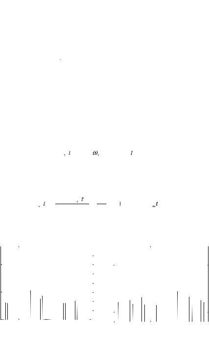
Leeson has developed a model that describes the origins of phase noise in oscillators [Lee66]; since it closely fits experimental data, the model is widely used in describing the phase noise of the oscillators [Roh83], [Man87]. In the model, the sampling clock signal (oscillator output) is phase modulated by a sine wave of frequency f
y ( |
t |
) |
|
cos( |
ω |
t |
|
β sinω |
|
|
t |
), |
(7.52) |
|
|
|
|
||||||||||
|
|
|
where is the sampling clock frequency of DDS, β is the maximum value of the phase deviation, is the offset frequency. The spectrum of the sampling clock signal is shown in Figure 7-7.
The frequency of the sampling clock signal is
f (t) |
d (θ (t)) |
= |
2π (ω β ω cosω ). |
(7.53) |
2π dt |
The DDS could be described as a frequency divider, and so the output frequency of the DDS is
POWER SPECTRUM
|
0 |
|
|
|
|
|
|
-10 |
|
|
|
|
|
dBc) |
-20 |
|
|
|
|
|
|
|
|
|
|
|
|
( |
|
|
|
|
|
|
POWER |
-30 |
|
|
|
|
|
RELATIVE |
-40 |
|
|
|
|
|
|
-50 |
|
|
|
|
|
|
-60 |
|
|
|
|
|
|
-70 |
|
|
|
|
|
|
-80 |
400 |
800 |
1200 |
1600 |
2000 |
|
|
FREQUENCY BIN
Figure 7-5. Discrete Fourier transform of the DDS output sequence for j = 12, k = 8 and ∆P = 619.
POWER SPECTRUM
|
0 |
|
|
|
|
|
|
|
-10 |
|
|
|
|
|
|
) |
|
|
|
|
|
|
|
(dBc |
-20 |
|
|
|
|
|
|
POWER |
-30 |
|
|
|
|
|
|
RELATIVE |
|
|
|
|
|
|
|
-50 |
|
|
|
|
|
|
|
|
-40 |
|
|
|
|
|
|
|
-60 |
|
|
|
|
|
|
|
-70 |
|
|
|
|
|
|
|
-80 |
400 |
800 |
1200 |
1600 |
2000 |
|
|
|
||||||
FREQUENCY BIN
Figure 7-6. Discrete Fourier transform of the DDS output sequence for j = 12, k = 8 and ∆P = 1121.

Sources of Noise and Spurs in DDS |
|
|
|
|
|
|
|
|
109 |
||||
f |
|
(t) |
∆P fs (t) |
fs (t) |
1 |
(ω |
|
+ β ω |
|
cosω |
|
t), |
(7.54) |
|
out |
|
2 j |
N |
2π |
|
out |
N |
m |
|
m |
|
|
where j is the word length of the DDS phase accumulator, ∆P is the phase increment word, N is the division ratio. The phase of the DDS output is
θ out (t) |
(ω out t + |
β |
sinω m t), |
(7.55) |
|||
|
|
||||||
|
|
N |
|
|
|
|
|
and the DDS output is |
|
|
|
|
|
|
|
yout (t) |
cos(ω out t + |
|
β |
sinω m t). |
(7.56) |
||
|
|
||||||
|
|
|
|
N |
|
||
Comparing (7.52) and (7.56), the modulation index is changed from β to β/N, but the offset frequency is not changed. The spectrum of the DDS sampling clock is given by inspection from the equivalent relationship
ys (t) cos(ωst + β sinωmt) |
Re{e j |
s t e jβ sin m t } |
|
Re e j s t ¦Ji (β )e ji |
|
|
(7.57) |
m t |
¦Ji (β )cos(ωst + iωmt) |
||
i − |
|
i |
− |
where Ji(β) are Bessel functions of the first kind. The spectrum of the DDS output is given by inspection from the equivalent relationship
|
(t) cos(ω out t + |
β |
sinω m t) |
|
|
|
e j out t e j |
β |
sin m t |
|
|
yout |
Re |
|
|
N |
|||||||
|
|
|
|
|
|||||||
|
|
N |
Nβ ) e ji |
|
|
|
|
(7.58) |
|||
|
|
|
|
|
|
|
|
||||
|
Re e j out t ¦J i ( |
m t |
|
|
¦Ji ( |
Nβ ) cos(ω out t + iω m t). |
|||||
|
i − |
|
|
|
|
i − |
|
|
|
||
The relative power of the DDS output phase noise at offset i m is from (7.57) and (7.58)
fs - fm fs fs + fm |
FREQUENCY |
Figure 7-7. Typical phase noise sidebands of an oscillator.

110
|
|
|
|
|
|
|
|
Pouti |
|
|
|
|
|
|
|
|
Psi |
If β << 1, then J |
0(β) |
1, J |
0(β/N) |
|||||
0 (i = 2, 3...), and |
|
|
|
|
|
|||
|
|
|
§ Pout1 |
· |
|
|
||
|
|
|
||||||
|
|
|
||||||
|
|
|
© |
Ps1 |
¹ |
|
dB |
|
|
|
|||||||
|
|
|||||||
|
|
§ |
Ji |
( |
β |
) |
· |
|
2 |
|
|
||||||||
|
|
|
|
|
|
|
|||
|
|
|
N |
|
|
|
|||
|
|
|
|
|
|
|
|
|
Ji (β )
©¹
1, J (β) β/2, J (β/N)
20 log10 (N) [ ]
]
Chapter 7
(7.59)
β/(2N) and Ji(β)
(7.60)
From the above equation, it can be seen that the relative power level of the DDS output phase noise depends on the ratio between the output frequency and sampling clock frequency. The output signal will exhibit the improved phase noise performance [Jen97], [Ana99]
f
nclk 20 log10 ( f s ). (7.61)
out
The DDS circuitry has a noise floor, which, at some point, will limit this improvement. An output phase noise floor of -160 dBc/Hz is possible, depending on the logic family used to implement the DDS [Qua90]. The frequency accuracy of the sampling clock is propagated through the DDS [Qua90]. Therefore, if the sampling clock frequency is 0.1 PPM higher than desired, the output frequency will be also higher by 0.1 PPM.
7.5 Post-Filter Errors
The sixth source of noise at the DDS output is the post-filter, eF, which is
needed to remove the high frequency sampling components. Since this postfilter is an energy storage device, the problem of the response time arises. The filter must have a very flat amplitude response and a constant group delay across the bandwidth of interest so that the perfectly linear digital modulation and frequency synthesis advantages are not lost. The output filter also affects the switching time of the DDS output.
REFERENCES
[Ana99] Analog Devices, "A Technical Tutorial on Digital Signal Synthesis," Application Note, 1999.
[Ben48] W. R. Bennett, "Spectra of Quantized Signals," Bell Sys. Tech. J., Vol. 27, pp. 446-472, July 1948.