

Vankka J. - Digital Synthesizers and Transmitters for Software Radio (2000)(en)
.pdf214 |
Chapter 10 |
Analog Integrated Circuits and Signal Processing, Vol. 29, No. 3, pp. 173180, Dec. 2001.
[Bos98] A. van den Bosch, M. Borremans, J. Vandenbussche, G. Van der Plas, A. Marques, J. Bastos, M. Steyaert, G. Gielen, and W. Sansen, "A 12 bit 200MHz Low Glitch CMOS D/A Converter," Proceedings of the IEEE Custom Integrated Circuits Conference 1998, pp. 249-252.
[Bos99] A. van den Bosch, M. Steyaert, and W. Sansen, "SFDR-Bandwidth Limitations for High Speed High Resolution Current Steering CMOS D/A Converters," Proceedings of the 6th IEEE International Conference on Electronics, Circuits and Systems 1999, Vol. 3, pp. 1193-1196.
[Bug00] A. Bugeja, and B.-S. Song, "A Self-Trimming 14-b 100-MS/s CMOS DAC," IEEE Journal of Solid State Circuits, Vol. 35, No. 12, pp.
1841-1852, Dec. 2000.
[Bug99] A. R. Bugeja, B. S. Song, P. L. Rakers, and S. F. Gillig, "A 14-b, 100-MS/s CMOS DAC Designed for Spectral Performance," IEEE J. SolidState Circuits, Vol. 34, No. 12, pp. 1719-1732, Dec. 1999.
[Bur01] M. Burns, and G. Roberts, "An Introduction to Mixed-Signal IC Test and Measurement," Oxford University Press, 2001.
[Chi86] K. Chi, C. Geisenhainer, M. Riley, R. Rose, P. Sturges, B. Sullivan, R.Watson, R. Woodside, and M. Wu, "A CMOS Triple 100-Mbit/s Video D/A Converter with Shift Register and Color Map," IEEE Journal of SolidState Circuits, Vol. SC-21, pp. 989-995, Dec. 1986.
[Chi94] S.-Y. Chi, and C.-Y. Wu, "A 10-b 125-MHz CMOS Digital-to- Analog Converter (DAC) with Threshold-Voltage Compensated Current Sources," IEEE Journal of Solid State Circuits, Vol. 29, No. 11, pp. 13741380, Oct. 1994.
[Con00] Y. Cong, and R. Geiger, "Switching Sequence Optimization for Gradient Error Compensation in Thermometer-Decoded DAC Arrays," IEEE Transactions on Circuits and Systems-II: Analog and Digital Signal Processing, Vol. 47, No. 7, pp. 585-595, July 2000.
[Con02] Y. Cong, and R. L. Geiger, "Formulation of INL and DNL Yield Estimation in Current-Steering D/A Converters," in Proc. IEEE International Symposium on Circuits and Systems (ISCAS), May 2002, pp. III.149III.152.
[Con03] Y. Cong, and R. Geiger, "A 1.5V 14b 100MS/s Self-Calibrated DAC," Digest of Technical Papers of the IEEE International Solid-State Circuits Conference 2003, pp. 128-129.
[Cre89] A. Cremonesi, F. Maloberti, and G. Polito, "A 100-MHz CMOS DAC for Video-Graphic Systems," IEEE Journal of Solid State Circuits, Vol. 24, No. 3, pp. 635-639, June 1989.
Current Steering D/A Converters |
215 |
[Cro97] D. Crook, and E. Stroud, "Drive Circuit and Method for Controlling the Crosspoint Levels of a Differential CMOS Switch Drive Signal," U. S.
Patent 5,703,519, Dec. 30, 1997.
[Cro98] D.Crook, and R. Cushing, "Sources of Spurious in a DDS/DAC System," RF Design, pp. 28-42, April 1998.
[Ded02] I. Dedic, "Switch Driver Circuitry Having First and Second Output Nodes with a Current-Voltage Converter Connected There Between Providing Current Paths of First and Second Directions There Between and Switching Circuitry Connected Therewith," U. S. Patent 6,340,939, Jan. 22, 2002.
[Ded99] I. Dedic, "Differential Switching Circuitry," U. S. Patent 6,100,830, Aug. 8, 2000.
[Dor01] K. Doris, D. Leenaerts, and A. van Roermund, "Time Non Linearities in D/A Converters," Proceedings of the European Conference on Circuit Theory and Design, Vol. III, pp. 353-356, 2001.
[Dud97] F. Dudek, B. M. Al-Hashimi, and M. Moniri, "CMOS Equaliser for Compensating sinc(x) Distortion of Video D/A Converters," Electron. Lett., Vol. 33, No. 19, pp. 1618-1619, Sep. 1997.
[Ess97] K. Essenwanger, "Digital-to-Analog Converted and Method that Set Waveform Rise and Fall Times to Produce an Analog Waveform that Approximates a Piecewise Linear Waveform to Reduce Spectral Distortion," U. S. Patent 5,663,728, Sept. 2, 1997.
[Ess98] K. Essenwanger, "Slewer Fractional-Order-Hold: The Ideal DAC Response For Direct Digital Synthesis," Proceedings of the IEEE International Frequency Control Symposium 1998, pp. 379-389.
[Fal99] K. Falakshahi, C.-K. Yang, and B. Wooley, "A 14-bit 10Msamples/s D/A Converter Using Multibit Ȉǻ Modulation," IEEE Journal of Solid State Circuits, Vol. 34, No. 5, pp. 607-615, 1999.
[Ger97] J. Gersbach, "Self Calibrating Segmented Digital-to-Analog Converter," U. S. Patent 5,642,116," June 24, 1997.
[Gro89] D. W. J. Groeneveld, H. J. Schouwenaars, H. A. H. Termeer, and C. A. A. Bastiaansen, "A Self-Calibration Technique for Monolithic HighResolution D/A Converters," IEEE J. Solid-State Circuits, Vol. 24, No. 6, pp. 1517-1522, Dec. 1989.
[Gus00] M. Gustavsson, J. Wikner, and N. Tan, "CMOS Data Converters for Communications," Kluwer Academic Publishers, 2000.
[Han99] J. Hanna, "Circuit and Method for Calibrating a Digital-to-Analog Converter," U. S. Patent 5,955,980, Sept. 21, 1999.
[Hen97] P. Hendriks, "Specifying Communications DACs," IEEE Spectrum, Vol. 34, No. 7, pp. 58-69, July 1997.
[Her91] R. Herman, A. McKay, and A. Chao, "Synchronizing Switch Arrangement for a Digital-to-Analog Converter to Reduce in-Band Switching Transients," U. S. Patent 5,059,977, Oct. 22, 1991.
Current Steering D/A Converters |
217 |
[Mer94] D. Mercer, "A 16-b D/A Converter with Increaced Spurious Free Dynamic Range," IEEE Journal of Solid State Circuits, Vol. 29, No. 10, pp. 1180-1185, Oct. 1994.
[Mer97] D. Mercer, D. Reynolds, D. Robertson, and E. Stroud, "Skewless Differential Current Switch and DAC Employing the Same," U. S. Patent 5,689,257, Nov. 18, 1997.
[Mik86] T. Miki, Y. Nakamura, M. Nakaya, S. Asai, Y. Asaka, and Y. Horiba, "An 80-MHz 8-bit CMOS D/A-Converter," IEEE Journal of Solid State Circuits, Vol. 21, No. 6, pp. 983-988, Dec. 1986.
[Nak91]Y. Nakamura, T. Miki, A. Maeda, H. Kondoh, and N. Yazawa, "A 10-bit 70 MS/s CMOS D/A converter," IEEE J. Solid-State Circuits, Vol. 26, pp. 637–642, Apr. 1991.
[Ngu92] T. Nguyen, "Spike Current Reduction in CMOS Switch Drivers," U. S. Patent 5,089,728, Feb. 18, 1992.
[Pel89] M. Pelgrom, A. Duinmaijer, and A. Welbers, "Matching Properties of MOS Transistors," IEEE Journal of Solid State Circuits, Vol. 24, No. 5, pp. 1433-1440, Oct. 1989.
[Pla99] G. Van der Plas, J. Vandenbussche, W. Sansen, M. Steyaert, and G. Gielen, "A 14-bit Intrinsic Accuracy Q2 Random Walk CMOS DAC," IEEE J. Solid-State Circuits, Vol. 34, No. 12, pp. 1708–1718, Dec. 1999.
[Rad00] R. Radke, and A. Eshraghi, "A 14-Bit Current Mode SD-DAC Based Upon Rotated Data Weighted Averaging," IEEE Journal of Solid State Circuits, Vol.35, No. 8, pp. 1074-1084, Aug. 2000.
[Raz95] B. Razavi, "Principles of Data Conversion System Design," IEEE Press, 1995.
[Sam88] H. Samueli, "The Design of Multiplierless FIR Filters for Compensating D/A Converter Frequency Response Distortion," IEEE Trans. Circuits and Syst., Vol. 35, No. 8, pp. 1064-1066, Aug. 1988.
[Sch03] W. Schofield, D. Mercer, and L. St. Onge, "A 16b 400MS/s DAC with -80dBc IMD to 300MHz and -160dBm/Hz Noise Power Spectral Density," Digest of Technical Papers of the IEEE International Solid-State Circuits Conference 2003, pp. 126-127.
[Sch04] B. Schafferer, and R. Adams, "A 3V CMOS 400mW 14b 1.4GS/s DAC for Multi-Carrier Applications," ISSCC Digest of Technical Papers, February 2004, San Francisco, USA, pp. 360-361.
[Sch88] H. Schouvenaars, D. Wouter, J. Groeneweld, and H. Termeer, "A Low-Power Stereo 16-bit CMOS D/A Converter for Digital Audio," IEEE Journal of Solid State Circuits, Vol. 23, No. 6, pp. 1290-1297, Dec. 1988.
[Sch97] W. Schnaitter, "Switchable Current Source for Digital-to-Analog Converter (DAC)," U. S. Patent 5,598,095, Jan. 1997.
[Sed91] A. Sedra, and K. Smith, "Microelectronic Circuits," 3rd edition, Saunders College Publishing, 1991.
Chapter 11
11. PULSE SHAPING AND INTERPOLATION FILTERS
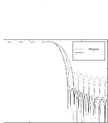
Different methods of designing the pulse shaping filters are reviewed in this chapter. In the digital modulators, phase distortion cannot be tolerated, thus the filters are required to have a linear phase response. A FIR filter can be guaranteed to have an exact linear phase response if the coefficients are either symmetric or antisymmetric about the center point. Three FIR filter structures (direct form, transposed direct form and hybrid form) are presented. The quantization effects and scaling methods within the fixed point FIR architectures are reviewed. Using canonic signed digit (CSD) coefficients, the FIR filtering operation can be simplified to add and shift operations. The well known carry save (CS) numbers are very attractive for VLSI implementation since the basic building block for arithmetic operations is a simple full adder. The multirate signal processing is particularly important in the digital modulator, where sample rates are low initially and must be increased for efficient subsequent processing. The efficient filter structures for the multirate signal processing (polyphase filters, halfband filters and comb filters) are presented. Taking advantage of the fact that in the modulator data streams in the I and Q paths are processed with the same functional blocks (see Figure 16-6), a further hardware reduction can be achieved by pipeline interleaving techniques.
11.1 Pulse Shaping Filter Design Algorithms
The pulse shaping filter design has two main objectives: minimization of the inter symbol interference (ISI) and maximization of the adjacent channel leakage power ratio (ACLR) [Che82], [Sam88], [Sam91], [Mor95]. [Sam88] and [Sam91] present two iterative algorithms that allow to the design of an overall filter of a given order N (an even number) with zero ISI and linear phase. The attenuation in the stopband is minimized. In [Sam88], only equiripple filters are considered and linear programming is used for deter-

220 Chapter 11
mining the filter taps. [Sam91] introduces a ripple weighting vector that allows arbitrary magnitude transfer functions to be designed, and uses equations instead of inequalities. Both [Sam88] and [Sam91] illustrate how to design a Nyquist filter that can be subsequently split into a transmitter and a receiver filter. [Sam88] and [Sam91] provide zero-ISI solutions but nonlinear phase characteristics. In [Mor95], the matched filter condition, i.e. identical transmit and receive filters with time reversal, is relaxed in order to obtain two linear phase transmit and receive filters and zero ISI in the composite filter. The transmit and the receive filters have different lengths. In [Che82], Chevillat and Ungerboeck present nonlinear optimization techniques for designing transmit and receive filters that result linear phase solutions with a non-zero-ISI [Che82].
The N-tap transmit filter is characterized by the coefficient vector h = (h0, h1, ..., hN-1)T, which is clocked at the rate M/ T corresponding to an oversampling ratio M. The receive filter (hr) is a K tap filter, which is M times over-sampled from the root raised cosine function. The transmit filter is convolved with the receive filter. Ideally, the result of the convolution will be an ideal raised cosine filter. There will be an EVM due to the truncation of the receive filter impulse response, if the length of the receive filter is short. It is therefore better to use a long receive filter so that the transmit filter will dominate the EVM.
The transmit and receive filter lengths are assumed to be either even or odd, so as to have one middle sample for decision in the composite pulse RC(n). The convolution of the transmitter and receiver filters should satisfy
the zero inter-symbol interference constraint: |
|
|
||
RC( ) 0 |
± lM |
l |
2 L |
(11.1) |
where nc is the center tap and M is the over-sampling ratio. The center tap is (N+K-2)/2. The total number of the terms in (11.1) is 2L, where L = ¬nc/M¼ and ¬x¼ denotes the integer part of x. The equation (11.1) can be written as
|
|
N |
1 |
|
|
|
|
|
|
RC( |
|
Ml) ¦hi hri |
|
Ml |
h T Sl hr l ± ± 2 |
|
± L |
(11.2) |
|
|
|
|
|||||||
|
|
i |
0 |
|
|
|
|
|
|
where the elements of the "shift" matrices Sl are zero, except si k(l) = 1 for i k = (N K)/2 + Ml [Che82]. The "shift" matrices Sl are N K matrices.
The passband ripples of the linear phase half-band filters (interpolation filters in Figure 16-6) cause EVM as well, which could be partly compensated for by predistortion of the pulse shaping filter. The receive filter (hr) could be convolved with the interpolation filters. This convolution could be calculated with the noble identities [Vai93]. The result is decimated back to the M over-sampled ratio and convolved with the transmit filter in (11.2).
One code channel is transmitted, when the EVM is measured. The EVM consists of two components, which are mutually uncorrelated:

Filter Design Algorithms |
|
|
|
|
|
|
221 |
|
L |
|
|
|
|
|
|
2 |
¦(h |
T |
Sl |
|
2 |
2 |
(11.3) |
EVM |
|
hr ) |
|
+ δ e |
l L l≠0
whereδ e2 is the quantization noise due to finite word length effects. The D/A converter dominates this quantization noise, because it is the most critical component. The ISI term is
|
L |
|
|
|
|
δ ISI2 |
¦ (hT Sl |
hr)2 |
hT W h |
||
|
l |
L |
|
|
|
|
l≠0 |
|
|
|
(11.4) |
|
|
|
L |
|
|
|
|
|
|
|
|
where W |
¦Sl |
hr (Sl |
hr)T |
||
|
|
l |
L |
|
|
|
|
l |
≠ 0 |
|
|
and W is a N N matrix. A linear constraint is added to guarantee proper scaling of the pulse peak
RC(nc ) hT S0 hr 1 |
(11.5) |
The lowpass channel energy (Ec) from dc to f (the cut-off frequency of the lowpass channel) is
|
|
|
f |
|
|
f |
b |
|
|
N − 1 |
N − 1 |
|
|
f |
f |
b |
|
|
||||||||
|
Ec |
|
³H ( f ) 2 df ¦ ¦hi hk |
³e j2 |
f (i k ) T / M |
|||||||||||||||||||||
|
|
|
df |
|||||||||||||||||||||||
|
|
|
f = f |
b |
|
|
i |
0 k 0 |
|
|
f |
f |
b |
|
(11.6) |
|||||||||||
|
|
|
|
|
|
|
|
|
|
|
|
|
|
|
|
|
|
|
|
|
|
|
|
|
|
|
|
|
|
N |
1 |
|
|
N |
1 |
|
|
|
|
|
|
|
|
|
|
|
|
|
|
|
|
||
|
|
|
¦ ¦hi hk rik |
hT R h |
|
|
|
|
|
|
|
|
|
|
|
|||||||||||
|
|
|
i= 0 |
|
|
k = 0 |
|
|
|
|
|
|
|
|
|
|
|
|
|
|
|
|||||
where R is a N N matrix with elements |
|
|
|
|
|
|
|
|
|
|||||||||||||||||
|
|
|
|
|
|
2 f |
b |
|
|
|
|
|
|
|
|
|
|
|
i |
k |
|
|||||
|
|
rik |
|
|
|
sin(2π f |
b |
(i |
k) T / M ) |
|
|
|
|
|
i ≠ k |
(11.7) |
||||||||||
|
|
|
|
|
|
|
|
|
|
|
|
|
|
|
|
|
||||||||||
|
|
|
|
|
|
|
|
|
|
π (i |
k) T / M |
|
|
|
|
|
|
|
|
|||||||
|
|
|
|
|
|
|
|
|
|
|
|
|
|
|
|
|
|
|
|
|
||||||
|
|
|
|
|
|
|
|
|
|
|
|
|
|
|
|
|
|
|
|
|
||||||
The stopband energy (Es) from f |
|
(stopband corner frequency) to M/(2T) is |
||||||||||||||||||||||||
|
||||||||||||||||||||||||||
|
|
f |
M /(2T ) |
|
|
N 1 |
N |
1 |
|
f |
M /(2T ) |
|
|
|||||||||||||
Es |
2 |
|
³H ( f ) 2 df 2¦ ¦hi hk |
|
|
|
³e j2 |
f (i |
k ) T / M df |
|||||||||||||||||
|
|
|
|
|
||||||||||||||||||||||
|
|
|
f |
|
|
fs |
|
|
i 0 |
k |
0 |
|
|
f fs |
|
(11.8) |
||||||||||
|
|
|
|
|
|
|
|
|
|
|
|
|
|
|
|
|
|
|
|
|
|
|
|
|
|
|
|
|
N |
1 |
N |
1 |
|
|
|
|
|
|
|
|
|
|
|
|
|
|
|
|
|
|
|||
|
|
¦ ¦hi hk vik |
hT V h |
|
|
|
|
|
|
|
|
|
|
|
||||||||||||
|
|
i 0 |
k |
0 |
|
|
|
|
|
|
|
|
|
|
|
|
|
|
|
|
|
|
||||
where V is a N |
|
|
N matrix with elements |
|
|
|
|
|
|
|
|
|
||||||||||||||
|
|
M / T |
|
|
|
|
2 fs |
|
|
|
|
|
|
|
|
|
|
|
|
|
i |
k |
||||
vik |
|
sin(π (i |
k)) |
sin(2π fs |
(i k) T / M ) |
i |
(11.9) |
|||||||||||||||||||
|
|
π (i |
|
k) T / M |
|
π (i |
k) T / M |
|
|
|
|
|
|
≠ k |
||||||||||||
|
|
|
|
|
|
|
|
|
|
|
|
|||||||||||||||
|
|
|
|
|
|
|
|
|
|
|
|
|||||||||||||||


 /2
/2


