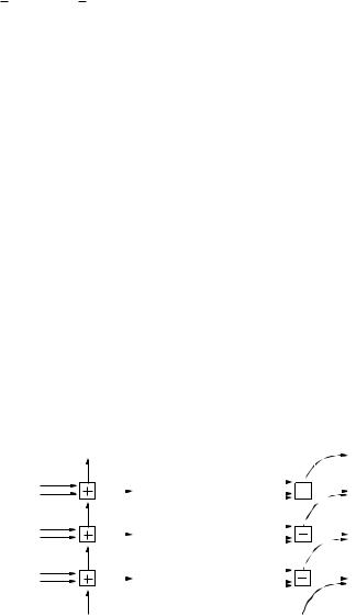
the number of taps N is odd and ¬N/2 ¼ if N is even. ¬x¼ stands for the integer part of x. In the folded regular direct form, the number of bits needed in the delay elements is defined by the number of input bits rather than the required word length of the filter, which may lead to a reduced amount of hardware. This structure is suitable for the programmable filter designs, because the effect of changing the filter coefficients is seen immediately or simultaneously at the filter output.
The long critical path causes problems in the high-speed systems when a short cycle-time is desired. However, this can be overcome by pipelining at the expense of an increased amount of hardware. The subexpression sharing method [Har96] can be applied easily, which reduces the amount of hard-
ware
11.3 Transposed Direct Form Structure of FIR Filter
The structure of the folded transposed direct form FIR filter is presented in Figure 11-3 In this case, as well as in the folded direct form filter described in Section 11.2, folding the taps reduces the amount of hardware. As can be clearly seen from Figure 11-2 and Figure 11-3, the maximum delay path is considerably shorter in the transposed form realization, resulting in a faster performance. The subexpression sharing method [Har96] can be applied easily, which reduces the amount of hardware.
A shortcoming of this structure is that if the filter coefficients are changed, the effect is spread over the multiple number of clock cycles, resulting in this structure being unsuitable for the programmable filter applications, when an immediate response to the change of the coefficients is required. Another problem of the transposed direct structure relates to the location of the delay elements in the output path of the filter. Because of the ad-
x(n)

 Z-1
Z-1 


 Z-1
Z-1 

Figure 11-3 Folded transposed direct form FIR filter (N is odd).
Filter Design Algorithms |
225 |
ditions, the delay elements might have to be implemented with a larger word length than in the direct structure counterpart [Haw96]. Hence, they require a larger area and consume more power. Anyhow, the necessity of enlarging the word length depends on the filter coefficients and is not always necessary.
In the folded transposed direct structure, a large loading occurs on the input data bus since all taps are fed in parallel, as shown in Figure 11-3 If the taps are realized as the multiplierless signed digit representation described in Section 11.6, this problem becomes even worse, due to the sign bit extensions in the shift operations. Fortunately, this sign bit load can be avoided by using the constant vector addition method proposed in [Haw96].
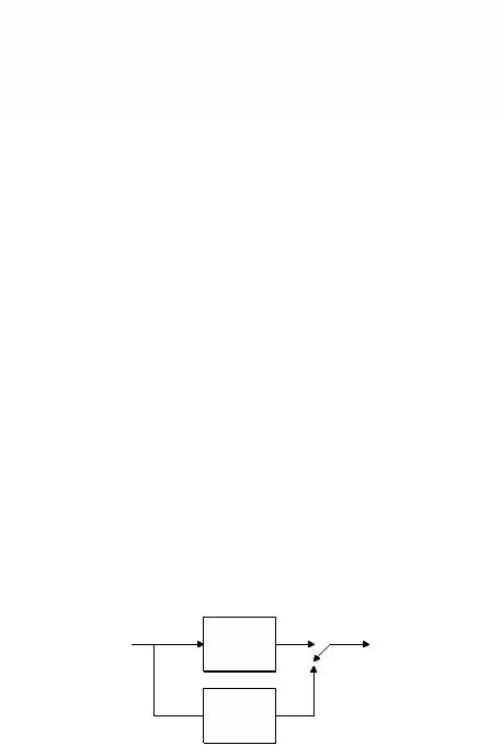
11.4 Hybrid Form
It is also possible to combine the filter structures described above into a socalled hybrid form filter [Lee96], [Kho01], [Hat01]. The purpose of this structure is to trade off the cycle-time requirement of an FIR filter with its area requirement. The hybrid form, depicted in Figure 11-4, can be thought of as being obtained from the direct structure by moving a minimum number of registers from the input path to the output path to satisfy the cycle-time requirement. Then the word length, and thus the required area of only a few registers, has to be increased. The cycle-time of a subsection, illustrated by a dash line in Figure 11-4, can be determined independently from the other subsections. An optimal design method of the hybrid form FIR filters is presented in [Kho01].
There are some restrictions on the advantages of the hybrid form. The benefit of using the hybrid form instead of the transposed direct form is not very large if the filter coefficients can be chosen such that the increase of the word length in the output path is not necessary and if the sign bit reduction technique [Haw96] is used to reduce the loading in the input path of the transposed direct form filter. The hybrid form can not be used in the programmable filters where an immediate or simultaneous response to the change of the filter coefficient is required. It is also very complicated to write a reusable hardware description of the hybrid form filter where the length of the filter is parameterizable. In case of a linear phase FIR filter,
x(n)  Z-1
Z-1  Z-1
Z-1  Z-1
Z-1 


 Z-1
Z-1
y(n) 


 Z-1
Z-1 


 Z-1
Z-1 


Figure 11-4 Hybrid form FIR filter.
folding the taps is possible only by introducing an extra delay element for every delay element moved to the output path. Anyhow, this increase of hardware is, in most cases, acceptable; also, the benefits of the hybrid form are more important.
11.5 Word Length Effects and Scaling
In order to get the best possible trade off between the signal to noise ratio at the output of the digital filter and the amount of hardware, the minimum accuracy needed has to be found. The noise sources are quantization errors and overflows in the FIR filters.
The mean and variance of the two's complement truncation error are [Con99]
me |
2 Bt |
2 |
Bo |
(11.13) |
|
2 |
|
|
|
|
|
įe2 2 2 Bt |
2 |
2 Bo |
(11.14) |
12 |
12 |
|
where Bt and Bo are the LSBs of the truncated word and the original, respectively. The DC offset at the FIR filter output due to the internal word length truncation is
N 1 |
|
mne me ¦h(n) |
(11.15) |
n 0 |
|
where h(n) is the filter coefficient. The DC offset can be removed by adding an appropriate offset at the output. The noise variance at the FIR filter output due to the internal word length quantization is
N |
1 |
|
įne2 įe2 ¦h(n) 2 |
(11.16) |
n |
0 |
|
The overflows in the filter output may be avoided, if the filter coefficients are scaled according to rule
s < |
1 |
(11.17) |
N |
1 |
xmax ¦h(n) |
n |
0 |
where xmax is the maximum of the input signal and s is the scaling factor. This scaling method is suitable for short FIR filters because the probability for overflow is high for a filter with a short impulse response. However, the above equation usually gives pessimistic values for the bandlimited signals. For narrowband signals, the filter coefficients are scaled according to rule
Filter Design Algorithms |
227 |
xmax max[ H (e jȦT ) ]
The two scaling methods just discussed are the ones used in practice. However, they lead only to a reasonable scaling of the filter. In practice, simulations with actual input signals should be performed to optimize the dynamic range.
A common scheme to reduce the size of overflow errors and their harmful influence is to detect numbers outside the normal range and limit them to either the largest or smallest representable number. This scheme is referred to as saturation arithmetic [Hwa75].
11.6 Canonic Signed Digit Format
A direct implementation of an N-tap FIR filter requires N multipliers, which consume a substantial amount of the chip area and power. Furthermore, the maximum speed of operation would be severely limited without pipelining. Implementing a fixed coefficient with a multiplier is very inefficient. In order to achieve the required throughput rate and to save hardware, a multiplierless filter coefficient architecture based on the canonic signed-digit (CSD) representation of coefficients is used. A coefficient can be recoded from a binary code to a signed-digit code containing the digits {-1, 0, 1}. In the signed-digit representation, the number is represented as the sums and differences of powers-of-two having the form
where L is the number of ternary bits in the signed-digit representation. The
Shift right 1 |
|
Shift right 4 |
|
Figure 11-5 Multiplication by a CSD-represented coefficient.
benefit of the CSD representations is that the multiplication operation can be realized by using only adders/subtractors and shift operations that can be realized with hardwired shifts. The minimum signed-digit representation refers to a code requiring the minimum number of non-zero digits. There may be more than one choice of minimum signed-digit representation. A CSD representation is defined as the minimum signed-digit representation for which no two adjacent non-zero digits ci exists. The CSD representation is unique. As an example, a multiplication by a CSD-represented coefficient 0.100101, where 1 denotes -1, equals to 2-1 - 2-4 + 2-6 = 0.4531. The implementation of this is illustrated in Figure 11-5. The programmable CSD coefficients have been presented in [Hau93], [Tat90], [Oh95], [Kho96], [Zha01], [Dua00], [Gra01].
The advantage of the CSD representation is that most of the numbers may be represented with many fewer non-zero digits than in a conventional binary code. The number of adders or subtractors required to realize a CSD coefficient is one fewer than the number of non-zero digits in the code. The accuracy of a CSD coefficient is controlled by the number of ternary bits L and by the maximum number of non-zero digits in the representation. Several algorithms have been presented for mapping the floating point or regular two's complement presentation to the CSD presentation [Zha88], [Sam89], [Li93], [Yag96], [Che99].
11.7 Carry Save Arithmetic
The well known carry save (CS) numbers are very attractive for VLSI implementation since the basic building block for arithmetic operations is a simple full adder. The CS-principle was developed in the late 40's and early 50's for fast digital computers. The basic idea is to postpone the time consuming carry propagation (CP) from a number of multiple additions. From the view of number representation the saving of the carry word results in a redundant number representation because of the multiple alternative repre-
|
|
s |
|
|
|
|
|
|
|
|
|
s |
i+1 |
|
|
i+1 |
|
|
|
|
|
|
|
|
|
|
|
|
|
|
|
|
c i+1 |
|
|
|
|
|
|
c i+1 |
|
|
|
|
|
|
|
|
|
|
|
|
|
|
|
|
|
|
s |
|
|
|
s |
|
|
|
|
|
|
|
|
|
i |
|
|
|
|
|
|
|
|
|
|
|
|
|
|
|
|
|
|
|
|
|
|
|
i |
|
|
|
c i |
|
i |
|
|
|
|
|
|
|
|
|
|
|
|
|
|
|
|
|
|
|
s |
|
|
|
|
|
|
|
|
|
|
|
|
|
|
s |
|
|
|
|
|
|
|
|
|
|
i-1 |
|
|
|
|
|
|
|
|
|
|
|
|
|
|
|
i-1 |
|
|
|
c i-1 |
c i-1 |
|
|
|
|
|
|
|
|
|
|
|
|
|
|
|
|
|
|
|
|
Figure 11-6. Carry ripple addition (left hand side) and 3-2 Carry Save addition (right hand side).
Filter Design Algorithms |
229 |
Figure 11-7. Addition of two Carry Save numbers (4-2 Carry Save addition).
nology. In today’s CMOS technologies the CS-arithmetic offers the potential of clock frequencies up to several hundred MHz. But in practice the maximum frequency is limited by clocking and I/O-bandwidth problems.
In recursive structures simple pipelining is not applicable. Here the CSarithmetic is a very attractive number representation, in order to deal with the fixed delay of the time critical recursive loops. The basic idea is to postpone the CP and therefore move the CP-path out of the recursive loops into parts of the structure where the timing restrictions are relaxed or where pipelining can be used.
A typical disadvantage of all redundant number representations is the problem of the sign detection, because a complete word level carrypropagation is still required in order to determine the sign of a redundant number. The same problem as with the sign detection occurs in saturation control. Difficulties with the sign detection and saturation control can nullify some, or all of the speed advantages of the CS-number representations (see section 6.3).
11.8 Polyphase FIR filters in Sampling Rate Converters
A FIR filter with a transfer function H(z) can be decomposed into its polyphase components as follows [Fli94]:
L 1 |
|
H (z) ¦ z l Hl (z L ), |
(11.20) |
l 0 |
|
where L is the number of polyphase components and, at the same time, the interpolation rate. One realization of a polyphase composed interpolation filter using two subfilters is shown in Figure 11-8. In this structure, the commutator takes care of the upsampling and right timing, so the separate up-samplers and the delay elements are not necessary. Using the polyphase decomposition, a lower clock rate can be used for the computation. The benefit of a lower clock rate appears as a possibility of using the pipelining/interleaving technique described in Section 11.11 or as a possibility of reducing the supply voltage in order to minimize the power dissipation. The
h(2k)
 h(2k+1)
Figure 11-8 Polyphase decomposed interpolation filter.

Filter Design Algorithms |
231 |
use of a lower clock rate also relaxes the timing constraints when synthesizing the design. As described in Section 11.2, in case of the linear phase FIR filters, the symmetry of the coefficients can be exploited using the folding method to reduce the area. If the subfilters are required to be symmetrical in order to make use of folding, the maximum number of the subfilters is two, when interpolating by the factor L = 2 and the number of filter taps is odd [Haw96]. In case of a larger number of subfilters, the subfilter coefficients are, in fact, symmetric or mirror image pairs, i.e. h0(n) = h1 (N - 1 - n), and these symmetries can be exploited to implement efficient calculation structures, similar to the folding method [Whi00].
11.9 Half-Band Filters for Interpolation
The interpolation filters are usually implemented with multirate FIR structures. There exists an well-known multirate architecture for implementing very narrow-band FIR filters, which consists of a programmable coefficient FIR filter, and half band filters followed by the cascaded-integrator-comb (CIC) structure [Hog81]. Unfortunately, the CIC structure is not particularly suitable for implementing wideband filters because the frequency response of the CIC filter does not have satisfactory stopband attenuation. Furthermore, the CIC filter introduces droop in the passband. The problems could be alleviated by increasing the ratio of the sampling frequency to the signal bandwidth. The half-band filters have frequently been applied to increase the pre-oversampling ratio. The half band filters have the center of their transition band at the quarter of the sampling frequency. They can be designed with the filter design algorithms with the following constraints
|
δ S |
δ P |
(11.21) |
|
ω S |
π − ω P |
|
|
where δS is the ripple in the stopband from ideal response, δP the ripple in the passband from ideal response, S the stopband edge frequency and P the passband edge frequency. A "trick" for their design has been introduced in [Vai87]. The half band filters have the property that every second of their coefficients, except the center coefficient (odd N), has zero value. Therefore, these filters can be implemented with approximately half the number of multiplications than arbitrary choices of filter designs.
11.10 Cascaded Integrator Comb (CIC) Filter
In [Hog81], an efficient way of performing decimation and interpolation was introduced. Hogenauer devised a flexible, multiplier-free filter suitable for hardware implementation that can also handle arbitrary and large rate
H ( f )
232 Chapter 11
changes. These are known as cascaded integrator comb filters, or CIC filters for short. Figure 11-9 shows the basic structure of the CIC interpolation filter. A CIC interpolator would be N cascaded comb stages with a differential delay of M samples per stage running at f /R, followed by a zero-stuffer, followed by N cascaded integrator stages running at f
 . The differential delay is a filter design parameter used to control the filter’s frequency response. In practice, the differential delay is usually held to M = 1 or 2. The transfer
function for a CIC filter at f |
|
is |
|
R M |
|
N |
ª |
R M |
1 |
k º |
N |
|
|
|
|
|
|
|
|
|
|
|
|
|
|
H (z) |
|
(1 |
z |
|
|
) |
|
¦z |
(11.22) |
|
(1 |
z |
1 |
) |
N |
|
|
|
¬ |
¼ |
|
|
|
|
|
|
|
|
|
|
|
|
|
|
|
|
|
k |
0 |
|
|
|
|
|
|
|
|
|
|
|
|
|
|
This equation shows that even though a CIC has integrators in it, which by themselves have an infinite impulse response, a CIC filter is equivalent to N FIR filters, each having a rectangular impulse response. Since all of the coefficients of these FIR filters are unity, and therefore symmetric, a CIC filter also has a linear phase response and constant group delay.
The power response at the output of the filter can be shown to be
ª sin(π M f ) º2 N
(11.23)
¬sin(π f / R) ¼
An example power response is given in Figure 11-10 for N = 4 stage CIC filter with a differential delay of M = 1 and a rate change factor of R = 16. The passband cutoff is at f = 0.19 with the aliasing/imaging bands centered
around the nulls at frequency of 1, 2, and 3 relative to the low sampling rate. For a CIC interpolator, the gain, G, at the ith stage is
|
|
|
2i |
|
|
|
|
|
|
|
|
|
|
i 1 2 ... N |
|
Gi |
22 N i (RM )i N |
|
|
|
N + 1 ... 2N |
(11.24) |
|
|
|
|
|
|
|
|
|
|
|
|
i |
|
|
|
|
|
|
|
|
|
|
|
|
|
|
|
|
|
|
|
R |
|
|
|
|
|
As a result, the register width, Wi, at ith stage is |
|
|
|
|
Wi |
[ |
|
|
|
|
|
|
|
|
|
|
|
|
] |
(11.25) |
|
|
|
|
|
|
|
|
|
|
|
|
|
|
|
|
|
|
|
|
|
|
|
|
|
|
|
|
|
|
|
|
|
where Bin is the input register width. The analysis of this is beyond the scope of this book, but is fully described in [Hog81].
In many CIC designs, the rate change R is programmable. Since the bit growth is a function of the rate change, the filter must be designed to handle both the largest and smallest rate changes. The largest rate change will dic-
|
|
|
|
|
Comb Section |
|
|
|
Integrator Section |
|
|
Stage 1 |
|
|
|
Stage N |
Stage N+1 |
Stage 2N |
fs/R |
|
|
|
|
|
|
|
|
|
N |
|
|
|
|
|
|
|
|
|
|
|
|
|
|
|
|
|
|
|
|
|
|
|
|
|
|
fs |
|
z |
-M |
|
|
|
z |
-M |
|
|
|
z |
-1 |
|
|
|
|
z |
-1 |
|
|
|
|
|
|
|
|
|
|
|
|
|
|
|
|
|
|
|
|
|
|
|
|
|
|
|
|
|
|
|
|
|
|
|
|
|
|
|
|
|
|
|
|
|
|
|
|
|
|
|
|
|
|
|
|
|
|
|
|
|
|
|
|
Figure 11-9. CIC interpolation filter.

Filter Design Algorithms |
233 |
tate the total bit width of the stages, and the smallest rate change will determine how many bits need to be kept in the final stage. In many designs, the output stage is followed by a shift register that selects the proper bits for transfer to the final output register.
Rounding or truncation cannot be used in CIC interpolators, except for the result, because the small errors introduced by rounding or truncation can grow without bound in the integrator sections.
Because of the passband droop, and therefore narrow usable passband, many CIC designs utilize an additional FIR filter at the low sampling rate. This filter equalizes the passband droop and performs a low rate change, usually by a factor of two to eight.
The economics of CIC filters derives from the following sources: 1) no multipliers are required; 2) no storage is required for filter coefficients; 3) intermediate storage is reduced by integrating at the high sampling rate and differentiating at the low sampling rate, compared to the equivalent implementation using cascaded uniform FIR filters; 4) the structure of combfilters is very “regular” consisting of two basic building blocks; 5) little external control or complicated local timing is required; 6) the same filter design can easily be used for a wide range of rate change factors, N, with the addition of a scaling circuit and minimal changes to the filter timing. Some problems encountered with CIC filters include the following. 1) Register widths can become large for large rate change factors, R. 2) The frequency response is fully determined by only three integer parameters (R M, and N),
Frequency Response of Fourth order CIC with M = 1, R = 16
|
0 |
1 |
|
-10 |
0 |
|
-1 |
|
|
|
-20 |
-2 |
|
-30 |
-3 0 0.05 0.1 0.15 |
|
Imaging Bands |
|
|
|
-40 |
|
|
-50 |
Pass- |
|
-60 |
bands |
|
|
-70
-80
-90
-1000 |
0.5 |
1 |
1.5 |
2 |
2.5 |
3 |
3.5 |
4 |
|
|
Frequency Relative to Low Sampling Rate |
|
Figure 11-10. Example frequency response for N = 4, M = 1, R = 16.


 s
s 


