

Vankka J. - Digital Synthesizers and Transmitters for Software Radio (2000)(en)
.pdf204 |
Chapter 10 |
transferred above the Nyquist band, then the reconstructing filter could remove them.
One method for this is shown in Figure 10-22 [Her91]. Two differential pairs are driven by alternating the control signals. Both differential pairs have a common current source, which is connected alternatively to the differential pairs at half the clock frequency. The outputs of the differential pair are connected together. Then one differential pair conducts at every even clock period, while the other at every odd period. The control signals are divided by the DEMUX to the two differential pairs so that the control signals cannot change its state when its differential pair conducts. Then the glitches due to the transitions cannot affect the output and consequently cause no harmonic distortions. Instead, the switches that control the current driven to the differential pairs change their states, which will cause a glitch at the output. Although this glitch is still generated when the switches are opened, this glitch occurs regularly, at the half sampling frequency, with amplitude that is dependent only on the value of the output. Therefore, the glitches contribute frequency components at the desired output frequency and at the half sampling frequency.
The circuit in Figure 10-22 does not reduce code related errors due to control signals feedthrough to the output. These code related errors could be cancelled by parallel dummy transistors (see Section 10.8.4).
The problem in this circuit is that the part of glitches caused by clock driven switches is not related to the output current. Therefore, part of the glitches is code related and causes distortion to the Nyquist band. The half clock related spurs are at the Nyquist frequency, therefore there might be difficulties in removing them. The half clock related spurs could be transferred to the sampling frequency by driving the lower switches at the clock frequency. In this case, the upper switches synchronization is more difficult. The circuit in Figure 10-22 increases complexity, because two extra demultiplexers and four switch transistors are needed. The extra switches between the output and ground reduce the output voltage swing range. Furthermore, the other differential pair source node is floating every other clock period, which increases the settling time.
10.8.6 Sample and Hold
One conceptual solution to the dynamic linearity problem is to eliminate the dynamic non-linearities of the D/A converter, all of which are associated with the switching behavior, by placing a track/hold circuit at the D/A converter output. The track/hold would hold the output constant while the switching is occurring, and track once the outputs have settled to their dc value. Thus, only the static characteristics of the D/A converter would show

Current Steering D/A Converters |
205 |
up at the output, and the dynamic ones would be attenuated or eliminated. The problem with this approach is that the track/hold circuit in practice introduced dynamic non-linearities of its own. A different approach, employing a return-to-zero (RZ) circuit at the output, is proposed in [Bug99], [Hyd03]. The output stage implements a RZ action, which tracks the D/A converter once it has settled, and then returns to zero. The problems of this approach are: large voltage steps cause extreme clock jitter and waveform fall/rise asymmetry sensitivity, large steps cause problems for the analog lowpass filter, and the output range (after filtering) is reduced by a factor of 2. To remedy these problems, current transients could be sampled to an external dummy resistor load, and settled current to external output resistor loads, by multiplexing two D/A converters [Bal87], [Van02].
The rise time is typically longer for a large step size than for a small step size, which causes distortions. This problem could be alleviated by the frac- tional-order-hold, where the transition is a fraction of the clock period and linear. It is easier to model this by real circuits than step functions. When the transition time is a fractional of the clock period, then output current transition time is constant [Ess97], [Ess98] and transition is linearly independent of the parasitic capacitances. Using this method, it is possible to get a 20 dB improvement at a 13 bit D/A converter distortion level at 0.4 f [Ess98]. The problem of the fractional-order-hold is that it is complex, and therefore requires extra chip area and consumes more power.
10.9 Timing Errors
There are three methods of reducing timing errors: the control signals synchronization, matching switch drivers loads and layout techniques.
10.9.1 Control Signals Synchronization
The control signals synchronization is needed even at low sampling frequencies, because the signal paths have different lengths even in the binary weighted D/A converter, where there is no longer additional logic. In the segmented D/A converters, the decoding delays make synchronization necessary. However, 8-bit D/A converters with a 65 MHz sampling frequency have been implemented without synchronization [Kim98]. The synchronization is implemented by the D flip-flop or latch, which are placed symmetrically near the switches. In [Mik86], [Bos98], [Pla99], [Bos01] the last latches are with current switches in the same matrix. This can cause the digital noise to be coupled to the output. The switch drivers can also do single ended to differential conversion, crosspoint setting and control voltage reduction [Tak91], [Bas98], [Bos98], [Pla99], [Bos01]. As the standard cell


Current Steering D/A Converters |
209 |
10.9.3 Layout
As the sampling frequency increases, the symmetry of the interconnections and cross coupling become important issues. For the methods presented in the previous sections to be useful, the signal paths from the D-flip-flop inputs to the current switches should be designed to be similar, while, to minimize the parasitic effects, the D-flip-flops should be located near the switches. The switches can be placed in a matrix [Mik86], [Tak91, [Bas98], [Pla99], [Bos01] such as the current sources, as this improves the matching between the switches. If the timing error minimization is not possible, the timing error should be made as random as possible between the switches, so that the error spectrum becomes noise [Dor01].
The supply fluctuations and clock jitter inside the chip cause current switches transition errors. Wider metal lines could minimize the supply voltage drops. Avoiding extensive buffering could reduce the clock jitter. The clock line sees a variable capacitive load, because the gate to source capacitance of the input transistors varies according to the states of switch drivers. If one global clock buffer is used, this will result in large code-dependent timing errors. The local clock buffers are used to reduce these codedependent timing errors [Fal99]. Dummy switch drivers were used in [Sch03], [Sch04] to ensure that same number of data transitions occur every clock cycle. Then the power supply of the switch drivers delivers a constant data-independent charge at the clock rate, and the clock line sees a fixed capacitive load. This was a key feature in achieving the exceptional performance levels in [Sch03], [Sch04].
10.10 Cascode Transistor
The output resistance of the output current source transistor is approximately [All87]
1 |
|
Rcs Ics Ȝcs |
(10.27) |
where λ 1/L The current source output resistance is related to the transistor channel length. The output current of the current source is inversely proportional to the channel length.
If the current switch transistors are in saturation region at the on-state, the output impedance of the current source is multiplied by the current switch voltage gain
gmsw |
2µ Cox |
Wsw |
Wsw Lsw |
(10.28) |
ǿcs λ2sw |
Lsw |

Current Steering D/A Converters |
211 |
of the cascode transistors attenuate the high frequency noise when the cascode is on [Mar98]. The high resistance also increases the output settling time; therefore the channel length should be minimum. This restricts the cascode transistors voltage gain to about 30 dB [Tei02], therefore it improves the linearity less than the cascoded transistor between the current switches and current sources. When the current switch is turned off, the cascode is turned off. The parasitic capacitance at the cascode transistor source is discharged through the cascode transistor, which reduces the output settling time at the positive voltage steps. This output rise and fall waveform asymmetry causes even harmonics, but this is partly cancelled at the differential output. However, the cascode transistors of the switches are used in [Tak91], [Bas98], [Mar98], [Zho01], [Xu99].
The cascode switch and current source transistors can be used together. The two cascode transistors reduce the output voltage range. Biasing the cascode transistors in the linear region could alleviate this problem, if the output impedance is not a limiting factor [Tak91]. It is quite easy to achieve DC impedance requirements, as the limiting factor is the output impedance degradation at high frequencies. If the current switches effect is taken into account, then the output impedance is
|
+ |
j ȦC0 |
|
|
|
Zimp Rsw (1 + gmsw (Rcs || C0 )) Rsw gmsw Rcs |
gmsw |
(10.29) |
|||
|
|||||
+ jȦC0 Rcs |
|||||
|
|
||||
where Rsw/Rcs is current switches/source resistance. According to the equation, the switch transistors add one zero at f = gmsw/(2 C0), but not affect the poles. The output impedance corner frequency does not depend on parasitic capacitance (C0) only, but also on the switches transconductance or current source resistance. As stated before, switch transistor size cannot be set arbitrarily. The zero is normally at high frequency, so it does not have a strong effect.
If the cascode transistors are between the current sources and switches as shown in Figure 10-26(a), then the output impedance becomes
|
|
(1 |
jω C |
(1 |
jω C0 |
|
|
|||||
|
|
+ |
|
|
|
+ |
|
|
|
|||
Zswcas Rsw Rcsc as Rcs gmsw gm csc as |
|
|
gmsw |
|
|
gm csc as |
|
(10.30) |
||||
(1 |
+ jω R |
cs |
C |
0 |
(1 |
+ jω R |
cscas |
C |
||||
|
|
|
|
|
|
|
|
|
|
|||
where Rcscas and gmcscas are cascode transistor resistance and transconductance, respectively. The cascode transistors add a pole at the frequency
1 |
|
f p 2π Rcsc as C |
(10.31) |
and zero at

Current Steering D/A Converters |
|
|
213 |
cal factors. The output impedance would then be |
|
||
ǽout Rswcas Rsw Rcscas Rcs gmswcas gmsw gm csc as |
|
||
(1+ jω C0 )(1+ |
jω C1 )(1+ |
jω C2 |
(10.34) |
gmsw |
gm csc as |
gmswcas |
|
(1 + jω Rcs C0 )(1 + jω Rsw C2 )(1 + jω Rcas C1
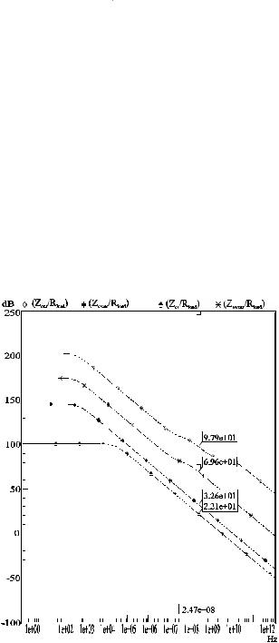
where half of the zeros and poles could be tuned by cascode transistors dimensions. In Figure 10-27, the 12bit D/A converter output impedance is shown with the different cascode structures (the wiring stray capacitances are taken into account). The curves from down to top are: current source output impedance (Zcs), cascode current source output impedance (Zcscas), cascode current source with current switch output impedance (Zswcas) and cascode current source with cascode switch output impedance (Zout). The current source transistor and cascode transistor has little difference at high frequencies due to lack of the wiring capacitance in the current source simulations. In Figure 10-27 the effect of the poles and zeros on the impedance can clearly be seen.
REFERENCES
[All87] P. Allen, and D. Holberg, "CMOS Analog Circuit Design," Oxford University Press, 1987.
[Bal87] G. Baldwin, et al., "Electronic Sampler Switch," U. S. Patent
4,639,619, Jan. 27, 1987.
[Bas91] C. Bastiaansen, D. Wouter, J. Groeneveld, H. Schouwenaars, and H. Termeer, "A 10-b 40 MHz 0.8- m CMOS Current-Output D/A Converter," IEEE Journal of Solid State Circuits, Vol. 26, No. 7, pp. 917-921, July 1991. [Bas97] J. Bastos, M. Steyaert, A. Pergoot, and W. Sansen, "Influence of Die Attachment on MOS Transistor Matching," IEEE Trans. Semiconduct.Manufact., Vol. 10, pp. 209–217, May 1997.
[Bas98] J. Bastos, A. Marques, M. Steyaert, and W. Sansen, "A 12-bit Intrinsic Accuracy High-Speed CMOS DAC," IEEE J. Solid-State Circuits, Vol. 33, No. 12, pp. 1959–1969, Dec. 1998.
[Bav98] N. van Bavel, "A 325 MHz 3.3V 10-Bit CMOS D/A Converter Core With Novel Latching Driver Circuit," Proceedings of the IEEE Custom Integrated Circuits Conference 1998, pp. 245-248.
[Bos01] A. van den Bosch, M. Borremans, M. Steyaert, and W. Sansen, "A 10-bit 1G Samples Nyquist Current-Steering CMOS D/A Converter," IEEE Journal of Solid State Circuits, Vol. 36, No. 3, pp. 315-324, Mar. 2001.
[Bos01a] A. Van den Bosch, M. Steyaert, and W. Sansen , "An Accurate Statistical Yield Model for CMOS Current-Steering D/A Converters,