

Vankka J. - Digital Synthesizers and Transmitters for Software Radio (2000)(en)
.pdfBlocks of Direct Digital Synthesizers |
173 |
[Nos01a] H. Nosaka, Y. Yamaguchi, and M. Muraguchi, "A Non-Binary Direct Digital Synthesizer with an Extended Phase Accumulator," IEEE Transactions on Ultrasonics, Ferroelectrics and Frequency Control, Vol. 48, pp. 293-298, Jan. 2001.
[Pal00] K. I. Palomaki, and J. Niittylahti, "Direct Digital Frequency Synthesizer Architecture Based on Chebyshev Approximation," in Proc. 34th Asilomar Conf. on Signals, Systems and Computers, 29 Oct.-1 Nov. 2000, Vol. 2, pp. 1639-1643.
[Pal03] K. I. Palomäki, and J. Niittylahti, "A Low-Power, Memoryless Direct Digital Frequency Synthesizer Architecture," Proceedings of the IEEE International Symposium on Circuits and Systems, May 2003, pp. II-77-80.
[Par00] M. Park, K. Kim, and J. A. Lee, "CORDIC-Based Direct Digital Synthesizer: Comparison with a ROM-Based Architecture in FPGA Implementation," IEICE Trans. Fundam., Vol. E83-A, No. 6 June 2000.
[Pii01] O. Piirainen, "Method of Generating Signal Amplitude Responsive to Desired Function, and Converter," U. S. Patent 6,173,301, Jan. 9, 2001. [Pre92] W. H. Press, S. A. Teukolsky, W. T. Vetterling, and B. P. Flannery, "Numerical Recipes in C, The Art of Scientific Computing," Second Edition, Press Syndicate of the University of Cambridge, New York, NY, USA,
1992.
[Qua91a] Qualcomm Q2334, Technical Data Sheet, June 1991.
[Ray94] Raytheon Semiconductor Data Book, Data Sheet TMC2340, 1994. [Rog96] R. Rogenmoser, and Q. Huang, "A 800-MHz 1- m CMOS Pipelined 8-b Adder Using True Single-Phase Clocked Logic-Flip-Flops," IEEE J. of Solid State Circuits, Vol. 31, No. 3, pp. 401-409, Mar. 1996.
[Rub89] P. W. Ruben, E. F. Heimbecher, II, and D. L. Dilley, "Reduced Size Phase-to-Amplitude Converter in a Numerically Controlled Oscillator," U. S. Patent 4,855,946, Aug. 8, 1989.
[Sai02] M. M. El Said, and M. I. Elmasry, "An Improved ROM Compression Technique for Direct Digital Frequency Synthesizers," Proceedings of the IEEE International Symposium on Circuits and Systems, Phoenix AZ, May 2002, pp. 437-440.
[Sch03] W. Schofield, D. Mercer, and L. St. Onge, "A 16b 400MS/s DAC with <-80dBc IMD to 300 MHz and <-160dBm/Hz Noise Power Spectral Density," ISSCC Digest of Technical Papers, February 2003, San Francisco, USA, pp. 126-127.
[Sch92] E. M. Schwarz, and M. J. Flynn, "Approximating the Sine Function with Combinational Logic," Asilomar Conf. on Signals, Syst. and Comput., Oct. 1992, pp. I-386-390.
[Sch99] M. J. Schulte, J. E. Stine, and J. G. Jansen, "Reduced Power Dissipation Through Truncated Multiplication," Proc. IEEE Workshop on LowPower Design, 1999, pp. 61-69.
174 |
Chapter 9 |
[Sha01] S. S. Shah, and S. Collins, "A 200 MHz Analogue-ROM Based Direct Digital Frequency Synthesizer with Amplitude Modulation," Proceedings of the IEEE International Symposium on VLSI Technology, Systems and Applications, Hsinchu, Taiwan, April 2001, pp. 53-56.
[Sod00] A. M. Sodagar, and G. R. Lahiji, "Mapping from Phase to SineAmplitude in Direct Digital Frequency Synthesizers Using Parabolic Approximation," IEEE Trans. Circuits Syst. II, Vol. 47, pp. 1452–1457, Dec. 2000.
[Sod01] A. M. Sodagar, and G. R. Lahiji, "A Pipeline ROM-Less Architecture for Sine-Output Direct Digital Frequency Synthesizers Using the Sec- ond-Order Parabolic Approximation," IEEE Transactions on Circuit and Systems II, Vol. 48, No. 9, pp. 850-857, Sep. 2001.
[Str02] A. G. M. Strollo, E. Napoli, and D. De Caro, "Direct Digital Frequency Synthesizers Using First-Order Polynomial Chebyshev Approximation," in Proc. of 28th European Solid-State Circuits Conf. (ESSCIRC 2002), Sept. 2002, pp. 527-530.
[Str03a] A. Strollo, D. De Caro, E. Napoli, and N. Petra, "Direct Digital Frequency Synthesis with Dual-Slope Approach," in Proc. 29th European SolidState Circuits Conference, Estoril, Portugal, Sept. 16-18 2003, pp. 397-400. [Str03b] A. G. M. Strollo, and D. De Caro, "Direct Digital Frequency Synthesizers Exploiting Piecewise Linear Chebyshev Approximation," Microelectronics Journal, Vol. 34, pp.1099-1106, Nov. 2003.
[Sun84]D. A. Sunderland, R. A. Strauch, S.S. Wharfield, H. T. Peterson, and C. R. Cole, "CMOS/SOS Frequency Synthesizer LSI Circuit for Spread Spectrum Communications," IEEE J. of Solid State Circuits, Vol. SC-19, pp. 497-505, Aug. 1984.
[Tan95a] L. K. Tan, and H. Samueli, "A 200 MHz Quadrature Digital Synthesizer/Mixer in 0.8 m CMOS," IEEE J. of Solid State Circuits, Vol. 30, No. 3, pp. 193-200, Mar. 1995.
[Tan95b] L. K. Tan, E. W. Roth, G. E. Yee, and H. Samueli, "A 800 MHz Quadrature Digital Synthesizer with ECL-Compatible Output Drivers in 0.8 m CMOS," IEEE J. of Solid State Circuits, Vol. 30, No. 12, pp. 1463-1473, Dec. 1995.
[Tho92]M. Thompson, "Low-Latency, High-Speed Numerically Controlled Oscillator Using Progression-of-States Technique," IEEE J. Solid-State Circuits, Vol. 27, pp. 113-117, Jan. 1992.
[Tie71] J. Tierney, C. Rader, and B. Gold, "A Digital Frequency Synthesizer," IEEE Trans. Audio and Electroacoust., Vol. AU-19, pp. 48-57, Mar. 1971.
[Tor01] F. Cardells-Tormo, and J. Valls-Coquillat, "Optimisation of Direct Digital Frequency Synthesisers Based on CORDIC," Electronic Letters, Vol. 37, No. 21, pp. 1278 -1280, Oct. 2001.
Chapter 10
10. CURRENT STEERING D/A CONVERTERS
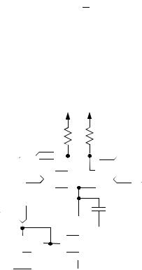
For high-speed and high-resolution applications (>50 MHz, >10 bits), the current source switching architecture is preferred, since it can drive a low impedance load directly without the need for a voltage buffer. The core of a current-steering D/A converter consists of an array of current sources that are switched to the output according to the digital input code. The current switches of the D/A converter could be implemented by CMOS differential pairs (see Figure 10-1), which are driven by the differential switching con-
trol signal Vctrl and V ctrl . The dominant parasitic capacitance (C0) is shown in Figure 10-1. The current is almost completely in one complementary output, when the voltage difference between the two switching transistors is [All87]
|
|
2Iss |
Lsw |
|
|
Vctrl |
Vctrl |
(10.1) |
|||
Cox |
Wsw |
||||
|
|
|
where Lsw is effective channel length, Wsw is effective channel width, is the mobility of electronics and Cox is the gate capacitance per unit area. Design for minimum voltage difference is not recommended because it is difficult to ensure that the minimum voltage is achieved in practice. Consequently, a safety margin is introduced. The current sources are implemented by current mirrors, for which the operation point is set by an internal or external current reference.
10.1 D/A Converter Specifications
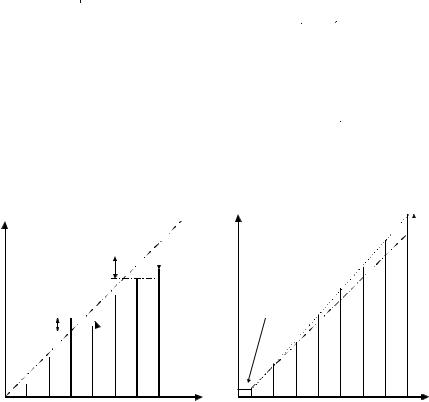
Figure 10-2 illustrates an offset, gain error, differential and integral nonlinearity (DNL and INL) as approximations to this transfer function. The output offset is usually defined as a constant DC offset in the transfer curve. The gain defines the full-scale output of the converter in relation to its refer-


 -
-

 DNL
DNL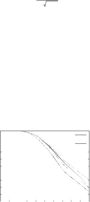
180 |
Chapter 10 |
normal distribution, the required accuracy is given by [Bos01a] |
|
σ (ILSB ) |
1 |
|
(10.7) |
ILSB |
2 C 2N − 1 |
where C depends only on the yield requirement and N is the number of bits. Various formulas for the C's dependence on the INL yield have been derived in the literature. Lakshmikumar has presented two rough bounds for INL yield estimation in binary-weighted D/A converters [Lak86], [Lak88]. The limitations of the two bounds were clearly shown in [Bos01a]. One is overly pessimistic, ignoring the strong correlation between different analog outputs, while the other is rather optimistic, considering only the contribution of the two mid-scale codes. Another formula proposed by van den Bosch for INL yield estimation is based on a nonstandard INL definition in which each current output is compared to the ideal value without correcting the gain error [Bos01a], although it is a well-known fact that a small gain error does not impact linearity. The formula therefore gives pessimistic results. The relationship between the INL yield requirement and the C for a fully segmented and binary weighted D/A converter, based on Monte Carlo simulations, has been presented [Con02]. For partially segmented architectures, corresponding values have not been presented. Monte Carlo simulations are therefore used to estimate the INL yield as a function of the unit current source standard deviation, as shown in Figure 10-3. In Figure 10-3, the INL performance, which is dependent on the segmentation level, is shown for four segmentation levels (0-12, 4-8, 8-4, 12-0), where the first number tells the number of the segmented bits. The fully segmented converter (12-0) does not give the worst yield shown in Figure 10-3; therefore, the thermometer and
100
|
|
|
|
|
|
|
|
|
|
12 - 0 |
|
|
90 |
|
|
|
|
|
|
|
|
8 |
- 4 |
|
|
|
|
|
|
|
|
|
|
|
|
4 |
- 8 |
|
|
|
|
|
|
|
|
|
|
|
0 |
- 12 |
|
80 |
|
|
|
|
|
|
|
|
|
|
|
|
70 |
|
|
|
|
|
|
|
|
|
|
|
|
|
|
|
|
|
|
|
|
|
|
|
|
|
|
60 |
|
|
|
|
|
|
|
|
|
|
|
|
50 |
|
|
|
|
|
|
|
|
|
|
|
|
|
|
|
|
|
|
|
|
|
|
|
|
40 |
|
|
|
|
|
|
|
|
|
|
|
|
30 |
|
|
|
|
|
|
|
|
|
|
|
|
20 |
|
|
|
|
|
|
|
|
|
|
|
|
10 |
|
|
|
|
|
|
|
|
|
|
|
|
0 |
0.3 |
0.4 |
0.5 |
0.6 |
0.7 |
0.8 |
0.9 |
1 |
1.1 |
1.2 |
||
0.2 |
||||||||||||
Unit Current Standard Deviation [%]
Figure 10-3. Yield estimation as function of the unit current source standard deviation
(with zero mean).
182 |
Chapter 10 |
from the matching point of view to generate the binary-weighted currents with equally sized current sources. Each binary-weighted current is constructed by connecting N unit current sources in parallel. The centroid of the composite sources is located at the center of the matrix [McC75], [Bas91]. This cancels the effects of linear process gradients across the matrix.
An unary decoded current sources are already equally sized, one can switch the current sources with a well-known symmetrical switching scheme [Mik86]. In this scheme, as shown in Figure 10-4(b), the current sources are arranged to average the spatial gradient errors in two directions, while the sequences for row and column selection are optimized independently. The switching optimization problem is thus reduced to a 1-D space. To compensate for both linear and quadratic errors, hierarchical symmetrical sequences were proposed (Figure 10-4(c)) [Nak91]. The switching optimization problem is also reduced to a 1-D space. The row-column and hierarchical symmetrical switching scheme are used in a 10 bit intrinsic accuracy D/A converter [Wu95], [Bav98]. The advantage of the row–column schemes are their simplicity for design and layout.
For the 2-D gradient error compensation, methods have been developed in which the current matrix is divided into regions (Figure 10-4(d)). The switching of regions is in the order of A, B, C, D; within the region the switching sequence is intended to compensate for quadratic and linear errors. The switching sequence could be determined by using algorithm techniques. Examples of methods are the "random walk" scheme [Pla99] and the INLbounded scheme [Con00], which is developed for switching sequence optimization for unary D/A converter arrays.
The most efficient method to compensate process gradients is to divide current source transistors into four transistors; their centroid is located at the center of the matrix (Figure 10-4(e)) [McC75], [Bas98], [Pla99]. Linear errors are cancelled and quadratic errors are divided into the four regions (A, B, C, D). The residual error is ¼ of the original error. The residual errors in regions (A-D) are compensated using either the row–column switching scheme [Lin98], [Bas98] or the "random walk" scheme [Pla99]. The current source transistor inside the region (A-D) is divided to four transistors; their centroid is located at the center of the matrix in a quad quadrant (Q2) scheme (Figure 10-4(f)) [Bos98], [Pla99]. Using this method, the residual error could be reduced four times. It is possible to divide the transistors further and place them in the common centroid scheme. The common centroid combined with some other switching scheme was used in the 10 and 12 bit D/A converters [Bas98], [Bos01]. The (Q2) scheme and random walk scheme was used in the 12 and 14 bit D/A converters [Bos98], [Pla99], respectively.
Figure 10-4 shows current sources switching schemes. The numbers at the edge of the matrix refer to the row and columns switching order. The

Current Steering D/A Converters |
183 |
number inside the matrix refers to the current sources switching order. The letters in Figure 10-4 refer to the regions switching order. In the common centroid methods, the letters refer to the regions.
10.2.3 Calibration
The gradient and random errors can be compensated using calibration [Gro89], [Ger97], [Han99], [Bug00], [Rad00], [Tii01], [Con03], [Sch03], [Hyd03] and dynamic element matching [Rad00]. Two approaches can be taken to calibrate out the errors: mixed signal or analog. In the mixed signal calibration, the main D/A converter has an additional trim D/A converter in parallel, which is controlled by a calibration circuit [Ger97], [Con03], [Sch03]. For each of the MSB codes, there is a calculated correction term that is converted with the trim D/A converter. The analog output of the trim D/A converter compensates the linearity errors in the main D/A converter. However, the trim D/A converter must also be designed for dynamic linearity performance. In the analog calibration, the currents sources are trimmable [Bug00], [Tii01], [Hyd03]. The analog calibration needs a D/A converter for changing the digital calibration values to the analog domain in [Bug00]. A large number of the MSB cells require complex refreshing circuitry [Bug00].
The calibration cycle that determines the correction terms is typically performed at startup. This is not always sufficient, since the component values may drift over time and change with temperature and supply voltage. Thus, the calibration has to be repeated from time to time, which requires suspending the normal operation of the converter. In many systems, the input signal contains idle periods, which can be used for calibration. This is not always possible and the calibration has to be performed in the background [Bug00]. Proper calibration can dramatically reduce the area of the current source array and hence the parasitic capacitances. The calibration also reduces sensitivities to process, temperature and aging, thus providing high yields.
10.3 Finite Output Impedance
Any non-ideal current source has a finite output impedance and can be modeled as shown in Figure 10-5, where k is the digital code, Rload is the load resistance, Cload is the load capacitance, Rlsb is the LSB current source resistance, Cout is the parasitic capacitance and Ilsb is the LSB current. The output current is [Mik86]