

Vankka J. - Digital Synthesizers and Transmitters for Software Radio (2000)(en)
.pdf132 |
|
|
|
|
|
|
|
Chapter 8 |
|
|
|
|
|
|
A2 / 2 |
|
|
|
|
P( f ) |
|
2 |
|
|
2 |
|
|
|
(8.53) |
|
|
|
|
|
|
||||
|
A2 / 2 |
|
|
|
|
|
|
||
|
|
( NPEF( f + fout ) |
2 |
+ NPEF( f fout ) |
2 |
) + |
NAEF ( f ) |
2 |
|
|
2 |
|
|
|
|||||
|
|
|
|
|
|
|
|
||
where A2/2 is the cosine wave power, NPEF f) is from (8.38) and NAEF f) is from (8.52).
A computer program (in Matlab) has been created to simulate the direct digital synthesizer in Figure 8-18. The simulated and theoretical from (8.53) signal to noise power spectrum densities are shown in Figure 8-20. The EF structures spread quantization noise to all the frequency bins as shown in Figure 8-20, because the coefficients of the EF structures in Figure 8-18 are "approximately" irrational numbers at the notch frequency (f otch /f
 = 0.3438).
8.4.2.2 Amplitude EF for Quadrature DDS
In the quadrature DDS (Figure 8-14), the complex amplitude EF transfer function is
|
|
|
|
|
|
|
|
|
|
|
|
|
|
|
|
|
|
|
|
|
|
|
|
|
|
|
|
|
|
|
|
|
|
), |
(8.54) |
|
|
|
|
|
|
|
|
|
|
|
|
|
|
|
|
|
|
|
|
|
|
|
|
|
|
|
|
|
|
|
|
|
|
|
|
and CA(z) is the amplitude error feedback filter in Figure 8-14. The spectral density of this amplitude quantization noise in (8.50) is given for z = ejω/fs
MAGNITUDE (dBc)
POWER SPECTRUM
0 
-20 
-40 
-60 
-80 
-100 
-120 |
0 |
5 |
10 |
15 |
20 |
25 |
30 |
35 |
40 |
|
|
|
|
OUTPUT FREQUENCY (MHz) |
|
|
|
||
Figure 8-21. Simulated power spectral density in Figure 8-19. Dashed line is from (8.56).
Spur Reduction Techniques in Sine Output Direct Digital Synthesizer |
133 |
|||||||||
|
CNAEF( f ) (( 2-2a |
2-2m ) |
CAEF ( f ) + E{cea |
2 }) |
1 |
|
|
|||
|
|
|
||||||||
|
|
6 |
|
|
π ( f fout ) |
|
|
fs |
|
(8.55) |
|
|
|
|
|
|
|
||||
|
(2 2a |
2-2m ) |
|
|
|
|
2 2m |
|
||
|
2 |
P |
) |
P |
1 |
|
||||
( |
|
|
(sin |
|
+ |
) |
|
|||
|
|
6 |
|
|
fs |
|
|
6 |
fs |
|
where E{cea2 }is from (7.38). The EF destroys the symmetry property of the amplitude error sequences. Therefore, amplitude quantization power spreads into frequency band 0 ≤ f < f . The power spectral density of the quadrature
Delta |
1 [T1] |
RBW |
5 kHz |
RF Att |
10 dB |
Ref Lvl |
- 75.32 dB |
VBW |
5 kHz |
|
|
- 10 dBm |
119.23847695 kHz |
SWT |
1 s |
Unit |
dBm |
-10 |
1 |
-20 |
-30 |
-40
1 AVG
-50
-60
-70
-80
-90 
-100 
-110
Center 13.5 MHz |
|
1 MHz/ |
|
Span 10 MHz |
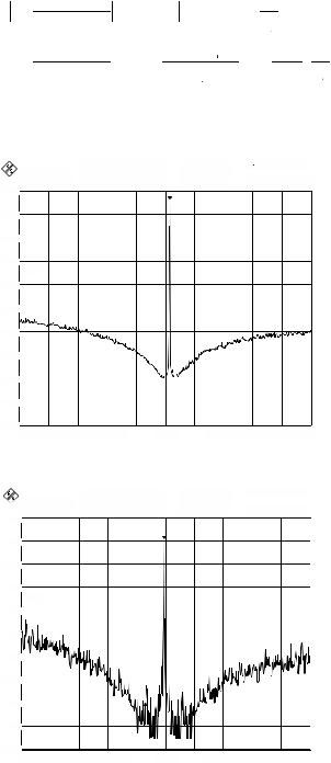
Figure 8-22. Spectrum of 13.7 MHz signal at 5-bit D/A converter output, where sampling frequency is 40 MHz.
|
Delta |
1 [T1] |
|
RBW |
5 kHz |
RF Att |
10 dB |
Ref |
Lvl |
- 70.68 |
dB |
VBW |
5 kHz |
|
|
- 10 |
dBm |
- 1.32264529 |
MHz |
SWT |
2 s |
Unit |
dBm |
-10 |
1
-20 |
-30
-40
1 AVG
-50
-60
-70
-80
1
-90
-100
-110
Center 20.1 MHz |
|
2 MHz/ |
|
Span 20 MHz |
Figure 8-23. Spectrum of 20 MHz signal at 4-bit D/A converter output, where sampling frequency is 40 MHz.

134 |
|
|
|
|
|
|
|
|
|
|
|
|
|
|
|
|
|
|
|
|
Chapter 8 |
output is from (8.50) and is given for |
= jω/fs |
||||||||||||||||||||
|
P |
|
f ) |
|
2 |
|
|
|
|
|
|
|
|
A 2 |
|
|
|
|
|
|
|
|
( |
|
|
|
|
|
|
|
|
|
|
|
|
|
|
(8.56) |
|||||
|
|
|
|
|
|
|
|
|
|
|
|
|
|
|
|
|
|
||||
|
|
|
|
|
|
A |
|
|
NPEF |
|
f |
|
|
f ) |
2 |
|
CNAEF |
|
f ) |
2 |
|
|
|
|
|
|
|
|
|
( |
|
|
+ |
( |
|
|
|||||||
where A2 is the quadrature wave |
power, NPEF f |
) is from (8.46) and |
|||||||||||||||||||
CNAEF f) is from (8.55).
A computer program (in Matlab) language was written to simulate the direct digital synthesizer in Figure 8-19. The simulated and theoretical (from 8.56) signal to noise power spectrum densities are shown in Figure 8-21. The spectrum has spurious signals in Figure 8-21 because of the phase EF filter coefficient is integer (2), but the EF still spreads part of the spur power to broadband noise.
8.5 Implementations
The cosine and quadrature DDS with phase and amplitude EF were implemented with the Altera FLEX 10KA-1 series devices [Fle98]. The cosine DDS (in Figure 8-18) with real phase and amplitude EF filters requires 282 (5% of the total) logic elements (LEs) in the EPF10K100A device. The quadrature DDS (in Figure 8-19) with real phase and complex amplitude EF filters requires 586 (11% of the total) LEs in the EPF10K100A device. The maximum operating frequency of the cosine and quadrature realization is 42 and 43 MHz, respectively. The D/A converters in Figure 8-13 and Figure 8- 14 were implemented using the MSB bits of the 14-bit D/A converter [Kos01].
8.6 Measurement Results
To evaluate the cosine and quadrature DDS with phase and amplitude EF, a test board was built and a computer program was developed to control the measurement. The phase increment and the EF filters tuning words are loaded into the test board via the parallel port of a personal computer. A spectrum plot of 13.7 MHz output from the cosine DDS with real tunable phase and amplitude EF (Figure 8-13) is illustrated in Figure 8-22. The power spectral density agrees with the simulation (and theoretical) results from Figure 8-20. A spectrum plot of 20 MHz output from the quadrature DDS with phase and complex amplitude EF (Figure 8-14) is illustrated in Figure 8-23. The power spectral density agrees with the simulation (and theoretical) results from Figure 8-21. The spur power is in tones around the carrier in Figure 8-21 and Figure 8-23.
Spur Reduction Techniques in Sine Output Direct Digital Synthesizer |
135 |
8.7 Conclusions
The reason why the dither techniques have not been applied very often to reduce the spurs due to the finite word length of the digital part of the DDS is because the effect of the D/A-converter non-linearities nullifies the contribution. The benefits of the high-pass filtered amplitude dither would be greater when it is used to randomize the D/A-converter non-linearities because the magnitude of the dither must be high in order to randomize the nonlinearities of the D/A-converter. The cosine and quadrature DDS with tunable phase and amplitude EF were designed and implemented. The drawback of the conventional phase EF is that it reduces the phase spurs only at DDS output frequencies which are near dc or half of the sampling frequency. New phase EF architectures with an arbitrary center frequency for cosine and quadrature output DDS are introduced. The EF structures can be used in conjunction with different phase to amplitude converter compression techniques.
REFERENCES
[Ble87] B. A. Blesser, and B. N. Locanthi, "The Application of NarrowBand Dither Operating at the Nyquist Frequency in Digital Systems to Provide Improved Signal-to-Noise Ratio over Conventional Dithering," J. Audio Eng. Soc., Vol. 35, pp. 446-454, June 1987.
[Can92] J. C. Candy, and G. C. Temes, "Oversampling Delta-Sigma Data Converters," IEEE Press, New York, 1992
[Car87] L. R. Carley, "An Oversampling Analog-to-Digital Converter Topology for High-Resolution Signal Acquisition Systems," IEEE Trans. Circuits and Syst., CAS-34, pp. 83-90, Jan. 1987.
[Con99] G. A. Constantinides, P. Y. K. Cheung, and W. Luk, "Truncation Noise in Fixed-Point SFGs [digital filters]," Electron. Lett., Vol. 35, No. 23, pp. 2012 -2014, Nov. 1999.
[Fla93] M. J. Flanagan, and G. A. Zimmerman, "Spur-Reduced Digital Sinusoid Generation Using Higher-Order Phase Dithering," Asilomar Conf. on Signals, Syst. and Comput., Nov. 1993, pp. 826-830.
[Fla95] M. J. Flanagan, and G. A. Zimmerman, "Spur-Reduced Digital Sinusoid Synthesis," IEEE Trans. Commun., Vol. COM-43, pp. 2254-2262, July
1995.
[Fle98] FLEX 10K Embedded Programmable Logic Family Data Sheet, Altera Corp., San Jose, CA, Oct. 1998.
[Gra93] R. M. Gray, and T. G. Stockholm, "Dithered Quantizers," IEEE Trans. Inform. Theory., Vol. 39, pp. 805-812, May 1993.
[Har95] F. Harris and B. McKnight, "Error Feedback Loop Linearizes Direct Digital Synthesizers," in Proc. IEEE 29th Asilomar Conf. on Signals, Sys-
136 |
Chapter 8 |
tems, and Computers, Pacific Grove, USA, 30 Oct. - 2 Nov. 1995, pp. 98102.
[Jas87] S. C. Jasper, "Frequency Resolution in a Digital Oscillator," U. S. Pat. 4,652,832, Mar. 24, 1987.
[Ker90] R. J. Kerr, and L. A. Weaver, "Pseudorandom Dither for Frequency Synthesis Noise," U. S. Pat. 4,901,265, Feb. 13, 1990.
[Kos01]M. Kosunen, J. Vankka, M. Waltari, and K. Halonen, "A Multicarrier QAM Modulator for WCDMA Base Station with on-chip D/A converter," Proceedings of CICC 2001 Conference, May 6-9 2001, San Diego, USA, pp. 301-304.
[Laz94] G. Lazzari, F. Maloberti, G. Oliveri, and G. Torelli, "Sinewave Modulation for Data Communication by Direct Digital Synthesis and Sigma Delta Techniques," European Trans. Telecommun. and Related Technologies, Vol. 5, pp. 689-695, Nov.-Dec. 1994.
[Lea91a] P. O' Leary, M. Pauritsch, F. Maloberti, and G. Raschetti, "An Oversampling-Based DTMF Generator," IEEE Trans. Commun., Vol. COM39, pp. 1189-1191, Aug. 1991.
[Lea91b] P. O' Leary, and F. Maloberti, "A Direct Digital Synthesizer with Improved Spectral Performance," IEEE Trans. Commun., Vol. COM-39, pp. 1046-1048, July 1991.
[Lju87] L. Ljung, "System Identification: Theory for the User," Englewood Cliffs, NJ: Prentice-Hall, 1987.
[Nic88] H. T. Nicholas, H. Samueli, and B. Kim, "The Optimization of Direct Digital Frequency Synthesizer in the Presence of Finite Word Length Effects Performance," in Proc. 42nd Annu. Frequency Contr. Symp., June 1988, pp. 357-363.
[Qua91a] Qualcomm Q2334, Technical Data Sheet, June 1991.
[Rei91] V. S. Reinhardt, and et al., "Randomized Digital/Analog Converter Direct Digital Synthesiser," U. S. Pat. 5,014,231, May 7, 1991.
[Rei93] V. S. Reinhardt, "Spur Reduction Techniques in Direct Digital Synthesizers," in Proc. IEEE Int. Frequency Cont. Symp., June 1993, pp. 230241.
[Twi94]E. R. Twitchell, and D. B. Talbot, "Apparatus for Reducing Spurious Frequency Components in the Output Signal of a Direct Digital Synthesizer," U. S. Pat. 5,291,428, Mar. 1, 1994.
[Van01] J. Vankka, and K. Halonen, "Direct Digital Synthesizers: Theory, Design and Applications," Kluwer Academic Publishers, 2001.
[Van97] J. Vankka, "A Direct Digital Synthesizer with a Tunable Error Feedback Structure," IEEE Transactions on Communications, Vol. 45, pp. 416-420, April 1997.
[Van98] J. Vankka, M. Waltari, M. Kosunen, and K. Halonen, "Direct Digital Syntesizer with on-Chip D/A-converter," IEEE Journal of Solid-State Circuits, Vol. 33, No. 2, pp. 218-227, Feb. 1998.
Spur Reduction Techniques in Sine Output Direct Digital Synthesizer |
137 |
[Whe83] C. E. Wheatley, III, "Digital Frequency Synthesiser with Random Jittering for Reducing Discrete Spectral Spurs," U. S. Pat. 4,410,954, Oct.
18, 1983.
[Wil91] M. P. Wilson, and T. C. Tozer, "Spurious Reduction Techniques for Direct Digital Synthesis," IEE Coll. Digest 1991/172 on Direct Digital Frequency Synthesis, Nov. 1991, pp. 4/1-4/5.
[Zim92] G. A. Zimmerman, and M. J. Flanagan, "Spur Reduced Numeri- cally-Controlled Oscillator for Digital Receivers," Asilomar Conf. on Signals, Syst. and Comput., Dec. 1992, pp. 517-520.
Chapter 9
9. BLOCKS OF DIRECT DIGITAL SYNTHESIZERS
The direct digital synthesizer (DDS) is shown in a simplified form in Figure 4-1. In this chapter, the blocks of the DDS: phase accumulator, phase to amplitude converter and filter are investigated. The D/A converter was described in Section 10. The methods of accelerating the phase accumulator are described in detail. Different sine memory compression and algorithmic techniques and their trade-offs are investigated.
9.1 Phase Accumulator
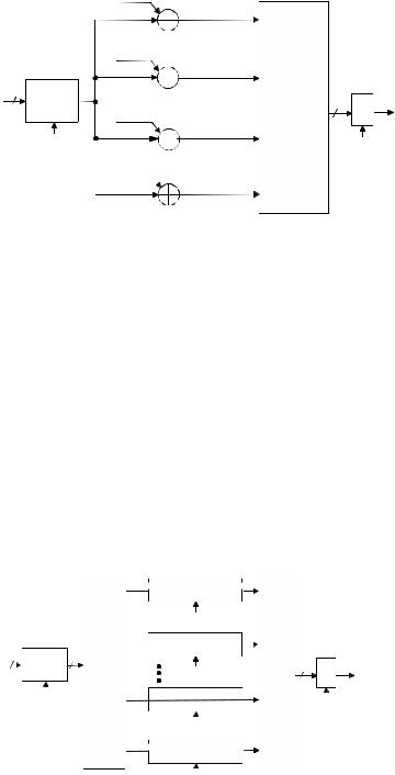
In practice, the phase accumulator circuit cannot complete the multi-bit addition in a short single clock period because of the delay caused by the carry bits rippling through the adder. In order to provide the operation at higher clock frequencies, one solution is a pipelined accumulator [Cho88], [Ekr88], [Gie89], [Lia97], as shown in Figure 9-1. To reduce the number of the gate delays per clock period, a kernel 4-bit adder is used in Figure 9-1, and the carry is latched between successive adder stages. In this way, the length of the accumulator does not reduce the maximum operating speed. To maintain the valid accumulator data during the phase increment word transition, the new phase increment value is moved into the pipeline through the delay circuit. All the bits of the input phase increment word must be delay equalized. The phase increment word delay equalization circuitry is thus very large. For example, in Figure 9-1, a 32-bit accumulator with 4-bit pipelined segments requires 144 D-flip-flops (DFFs) for input delay equalization alone. These D-flip-flop circuits would impact the loading of the clock network. To reduce the number of pipeline stages, a carry increment adder (CIA) [Kos99] and a conditional sum adder in [Tan95a] are used. To reduce the cycle time and size of pipeline stages further, the outputs of the adder and the D-flip- flops could be combined to form "logic-flip-flop" (L-FF) pipeline stages

140 |
Chapter 9 |
[Yua89], [Rog96], [Kos99]; thereby their individual delays are shared, resulting in a shorter cycle time and smaller area.
Pre-skewing latches with pipeline control are used to eliminate the large number of D-flip-flops required by the input delay equalization registers [Che92], [Lu93]. The cost of this simplified implementation is that the frequency can be updated only at f /PS, where PS is the number of the pipelined stages.
The phase increment inputs to the phase accumulator are normally generated by a circuitry that runs from a clock that is much lower in frequency than, and often asynchronous to, the DDS clock. To allow this asynchronous loading of the phase increment word, double buffering is used at the input of the phase accumulator.
The output delay circuitry is identical to the input delay equalization circuitry, inverted so that the low-order bits receive a maximum delay while the most significant bits receive the minimum delay. In Figure 9-1 the data from the most significant 12 bits of the phase accumulator are delayed in pipelined registers to reach the phase to amplitude converter with full synchronization. A hardware simplification is provided by eliminating the de-skewing registers for the least significant j k bits of the phase accumulator output. This is possible because only the k most significant phase bits are used to calculate the sine function. The only output bits that have to be delay equalized are those that form the address of the phase to amplitude converter. The processing delay is from the time a new value is loaded into the phase register to the time when the frequency of the output signal actually changes, and the pipeline latency associated with frequency switching is 9 clock pulses, see Figure 9-1.
In [Tho92], a progression-of-states technique, rather than pipelining, was incorporated as shown in Figure 9-2. The outputs of the phase accumulator are shown in (9.1)-(9.4) when the phase increment word is held constant for
∆P[28:31]
∆P 32 INPUTRE  GISTER
4 |
|
4 |
|
|
4 |
|
4 |
4 |
4 |
|
4 |
|
4 |
|
|
|
|
|||||||||
DFF |
|
DFF |
|
|
DFF |
DFF |
DFF |
DFF |
|
DFF |
DFF |
4 |
||||||||||||||
|
|
|
|
|
|
|
|
|
|
|
|
|
|
|
|
|
|
|
|
|
|
|
||||
|
|
|
|
|
|
|
|
|
|
|
|
|
|
|
|
|
|
|
|
|
|
|
|
DFF |
||
CLK |
|
CLK |
|
|
CLK |
CLK |
CLK |
CLK |
|
CLK |
CLK |
4 |
|
|
||||||||||||
|
|
|
|
|
|
|
|
|
|
|
|
|
|
|
|
|
|
|
|
|
|
|
|
|
|
|
|
|
|
|
|
|
|
|
|
|
|
|
|
|
|
|
|
|
|
|
|
|
|
|
CLK |
||
|
|
|
|
|
|
|
|
|
|
|
|
|
|
|
|
|
|
|
|
|
|
CLK |
DFF |
|||
|
|
|
|
∆ |
|
P[20:23] |
4 |
4 |
4 |
4 |
|
4 |
|
CARRY |
||||||||||||
|
|
|
|
|
||||||||||||||||||||||
|
|
|
|
|
|
|
|
|
|
|
|
|
||||||||||||||
|
|
|
|
|
|
|
|
|
|
|
DFF |
DFF |
DFF |
|
DFF |
DFF |
4 |
|||||||||
|
|
|
|
|
|
|
|
|
|
|
|
|
|
|
|
|
|
|
|
|
|
|
||||
|
|
|
|
|
|
|
|
|
|
|
|
|
|
|
|
|
|
|
|
|
|
|
|
DFF |
||
|
|
|
|
|
|
|
|
|
|
|
CLK |
CLK |
CLK |
|
CLK |
CLK |
4 |
|
|
|||||||
|
|
|
|
|
|
|
|
|
|
|
|
|
|
|
|
|
|
|
|
|
|
|
|
|
|
|
|
|
|
|
|
|
|
|
|
|
|
|
|
|
|
|
|
|
|
|
|
|
|
|
CLK |
||
|
|
|
|
|
|
|
|
|
|
|
|
|
|
|
|
|
|
|
|
|
|
CLK |
DFF |
|||
|
|
|
|
|
|
|
|
|
|
|
|
|
|
|
|
|
∆P[0:3] |
4 |
|
CARRY |
||||||
|
|
|
|
|
|
|
|
|
|
|
|
|
|
|
|
|
|
|
|
|
|
|||||
|
|
|
|
|
|
|
|
|
|
|
|
|
|
|
|
|
|
|
|
|
DFF |
4 |
||||
|
|
|
|
|
|
|
|
|
|
|
|
|
|
|
|
|
|
|
|
|
|
|
||||
|
|
|
|
|
|
|
|
|
|
|
|
|
|
|
|
|
|
|
|
|
|
|
|
DFF |
||
|
|
|
|
|
|
|
|
|
|
|
|
|
|
|
|
|
|
|
|
|
CLK |
4 |
|
|
||
CLK
4 P[28:31]
4 |
|
4 |
4 |
|
|
DFF |
|
DFF |
T |
|
|
O |
|
|
P |
|
|
H |
|
|
|
A |
|
|
S |
|
|
E |
|
|
T |
|
|
|
O |
|
|
A |
|
|
M |
|
|
P |
|
|
L |
|
|
IT |
|
|
U |
|
|
D |
|
|
E |
|
|
C |
|
|
O |
|
|
N |
|
|
V |
|
|
E |
P[20:23] |
R |
|
T |
||
|
|
E |
|
|
R |
CLK CLK
Figure 9-1. Pipelined 32-bit phase accumulator.

Blocks of Direct Digital Synthesizers |
141 |
four clock cycles. Holding the phase increment limits the phase increment
update rate. The outputs of the phase accumulator are |
|
|||||||||||||||||||||||||
P( |
|
) |
P( |
|
) |
∆P |
P( |
|
|
) |
|
|
∆P |
(9.1) |
||||||||||||
P( |
|
|
|
|
2) |
P( |
|
|
|
) |
∆P |
P( |
|
|
|
) |
2∆P |
(9.2) |
||||||||
P( |
|
|
|
|
3) |
P( |
|
|
|
2) |
∆P |
P( |
|
|
|
) |
3∆P |
(9.3) |
||||||||
P( |
|
|
4) |
P( |
|
|
3) |
∆P |
P( |
|
|
) |
4∆P |
(9.4) |
||||||||||||
where ∆P is the phase increment word and P(n) is the output of the phase accumulator at nth sampling instant. To generate P(n+2) and P(n+4) in (9.2) and (9.4), ∆P is shifted up 1bit and 2bits before they are added respectively. To generate P(n+3) in (9.3), P(n+2) and ∆P are used instead of 3∆P. The progression-of-states technique in Figure 9-2 demands D-flip-flop circuits and four adders so it has the area and power overheads. To increase the operation speed of the phase accumulator using the progression-of-states technique, the pipelining technique is used in [Yan02].
The use of parallel phase accumulators to attain a high throughput has been utilized in [Has84], [Gol90], [Tan95b]. The structure in Figure 9-3 uses a phase accumulator and four adders [Tan95b]. Four adders are required to make four sequential phase outputs P(n+1), P(n+2), P(n+3), P(n+4). The four phase outputs are generated by adding 0, ∆P, 2∆P, 3∆P phase offsets to the phase accumulator output. To generate every fourth sample at the phase accumulator output before adders in Figure 9-3, the phase increment word must be multiplied by four (4∆P).
The phase accumulator could be accelerated by introducing a Residue Number System (RNS) representation into the computation, and eliminating the carry propagation from each addition [Chr95]. The conversion and the re-conversion to/from the RNS representation reduces the gain in the computation speed.
|
|
|
|
32 |
|
|
|
|
|
|
x4 |
|
|
|
|
|
|
|
|
|
DFF |
|
|
|
|
|
|
|
|
|
|
|
|
|
|
|
|
|
|
CLK/4 |
|
|
|
|
|
|
|
|
32 |
|
|
|
|
|
|
|
|
DFF |
|
|
|
|
|
|
|
|
CLK/4 |
|
4 : 1 |
|
32 32 P[0:31] |
|
|
|
|
MUX |
||||
|
|
|
|
|
|
|
DFF |
|
|
|
|
|
32 |
|
|||
|
|
|
|
|
|
|
|
|
|
|
x2 |
|
|
|
|
CLK |
|
|
|
|
DFF |
|
|
|
||
|
32 |
|
|
|
|
|
||
|
|
|
|
|
|
|
|
|
|
|
|
|
CLK/4 |
|
|
|
|
∆P 32 32 |
|
|
32 |
32 |
|
|
|
|
DFF |
|
|
|
|
|
|
|
|
|
|
|
DFF |
|
|
|
|
|
|
|
|
|
|
|
|
|
|
CLK/4 |
|
|
|
CLK/4 |
|
|
|
|
|
|
|
|
|
|
|
Figure 9-2. 32-bit phase accumulator using a progression-of-states technique.
142 |
|
|
|
|
|
Chapter 9 |
|
|
0 |
|
|
|
|
|
|
∆P |
|
|||
4∆P 32 |
PHASE |
32 |
|
|
|
|
ACCU- |
|
|
|
|
||
|
|
|
4 : 1 |
|
32 32 |
|
|
MULATOR |
|
|
|
|
|
|
|
MUX |
DFF |
|||
|
|
2∆P |
||||
|
|
|
||||
|
CLK/4 |
|
|
|
|
CLK |
3∆P
Figure 9-3. 32-bit phase accumulator using parallel adders.
The frequency resolution is from (4.2), when the modulus of the phase accumulator is 2j. In this case, the implementation of the modulo operation is straight forward. Few techniques have been devised to use a different modulus [Jac73], [Gol88], [McC91b], [Gol96], [Har91], [Nos01a], [Uus01]. The penalty of those designs is a more complicated phase address decoding [Gol96]. The benefit is a more exact frequency resolution (the divider is not restricted to a power of two in (4.2), when the clock frequency is fixed [Gol96]. For example, 10 MHz is the industry standard for electronic instrumentation requiring accurate frequency synthesis [McC91b]. To achieve a one hertz resolution in these devices, the phase accumulator modulus must be set equal to 106 (decimal) [Jac73], [Gol88]. The modulus of the phase accumulator is variable in [McC91b], [Ell96], [Nos01a]. This allows a flexible output tuning resolution.
For a phase accumulator with phase truncated output, the only useful information produced by the adder below the truncation point is the carry-out signal. Therefore, the lower part of the phase accumulator can be replaced
PHASE to AMPLITUDE
CONVERTER
|
|
|
|
|
|
|
|
|
CLK/L |
|
|
|
|
|
|
|
|
|
|
|
|
|
|
|
|
|
|
|
|
|
|
|
|
|
|
|
|
|
|
|
|
PHASE to AMPLITUDE |
|
|
|
|
|
|
||
∆P j PHASE |
k |
CONVERTER |
|
|
|
|
|
|
|
|||||||
|
|
|
|
|
|
|
|
|
||||||||
|
|
ACCU- |
|
|
|
|
|
|
|
|
|
|
L : 1 |
|
|
|
|
|
L : 1 |
|
CLK/L |
|
|
|
|
m m |
|||||||
|
|
|||||||||||||||
|
|
MULATOR |
|
|
|
|
|
|
|
|||||||
|
|
|
|
DEMUX |
|
|
|
|
|
MUX |
|
DFF |
||||
|
|
|
|
|
|
|
||||||||||
|
|
|
|
|
|
|
|
|
|
|
|
|||||
|
|
|
|
|
|
|
|
|
|
|
|
|
|
|
|
|
|
|
CLK |
|
|
|
|
|
PHASE to AMPLITUDE |
|
|
|
|
|
CLK |
||
|
|
|
|
|
|
|
|
CONVERTER |
|
|
|
|
|
|
||
|
|
|
|
|
|
|
|
|
|
|
|
|
|
|
||
|
|
|
|
|
|
|
|
|
|
|
|
|
|
|
|
|
CLK/L
PHASE to AMPLITUDE
CONVERTER
CLK/L
Figure 9-4. A DDS using parallel phase to amplitude converters.