


α Series Simple Application Controllers |
Function Block Diagram (FBD) Programming 6 |
|
|
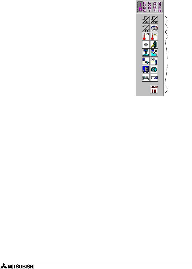
6.2Component Items (Icons) of the Program
Programs for the α series can be created and edited from the Program Edit Mode. Program Edit is the default mode for the AL-PCS/WIN-E. The α series is programmed by placing items on the FBD Base and connecting the various components together with the wiring analyzer. There are 8 types of system components that can be placed on the FBD base. A short description of the function and placement locations possible for the various components follows;
Digital Input Icon, Analog Input Icon, |
|
Digital Output Icon, Output Icon |
||||
Input Icon for AS-interface, System Bit, Operation Key |
|
for AS-interface, Control Bit |
||||
|
|
|
|
|
|
|
Function Block, Logic function Block
6.2.1FBD Base
The Function Block Diagram (FBD) base in the FBD Window provides the platform upon which the program for the α series is constructed. The FBD base consists of a large wiring area (lime green by default), a title box and input / output rectangles vertically along the right and left hand sides, respectively. Programming components are placed on the wiring area or in the rectangles, and connected by wires to construct the program of the α series.
6-2
α Series Simple Application Controllers |
Function Block Diagram (FBD) Programming 6 |
|
|
6.2.2Inputs
The types of input signals are the Digital Inputs, Analog Inputs and AS-interface bits. The icons can be found under the Input Signals Accessories Toolbar “IN” at the left of the FBD base.
1)The digital signals can be placed on the Input rectangles at the left of the FBD base or on the base itself. Each icon functions in the same way. The different icons have been developed to aid in the documentation and understanding of the program. Use an input icon that corresponds to the actual input device to be connected to the α series. The names of the signals will appear when the mouse arrow is placed on the icon.
2)The analog and temperature (from AL2-2PT-ADP or AL2- 2TC-ADP adapter) signals can only be placed in Input Rectangles I01 - I08.
Table 6.1: Applicable Analog Signals
Digital signals
Analog signals
Temperature signals
Digital signals
AS-interface bits
|
|
|
|
|
|
Series |
Signal |
Location |
|
|
|
|
|
|
|
α Series |
Analog |
AL-**M*-D model + AL-PCS/WIN-E Version 1.00 or later |
|
|
|
|
|
|
|
Temperature |
Not support |
|
|
|
|
|
||
|
|
|
|
|
|
|
Analog |
AL2-**M*-D model + AL-PCS/WIN-E Version 2.00 or later |
|
|
|
|
|
|
|
α2 Series |
|
AL2-14M*-*, AL2-24M*-* model (V2.00 or more) |
|
|
Temperature |
+ “AL2-2PT-ADP or AL2-2TC-ADP” |
|
|
|
|
|
||
|
|
|
+ AL-PCS/WIN-E Version 2.30 or later |
|
|
|
|
|
|
|
|
|
|
|
3)Four AS-interface bits, “LINK in” icon E01 - E04, are available when using the following location. These inputs can be placed anywhere on the FBD base and will not be counted toward the number of system Inputs.
Table 6.2: Applicable AS-interface module
|
|
|
|
|
Series |
Location |
|
|
|
|
|
|
α Series |
AL-20M*-* model + AL-PCS/WIN-E Version V1.30 or later |
|
|
|
|
|
|
α2 Series |
AL2-14M*-*, AL2-24M*-* model + AL-PCS/WIN-E Version V2.00 or later |
|
|
|
|
|
|
|
|
|
6-3
α Series Simple Application Controllers |
Function Block Diagram (FBD) Programming 6 |
|
|
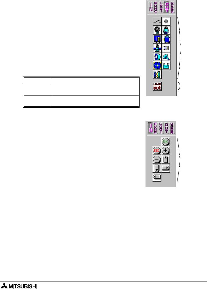
6.2.3Outputs
Output signals is the Digital Outputs and AS-interface bits. The icons can be found under the Output Signals Accessories Toolbar “Out” at the left of the FBD base.
1)The system outputs should be placed in the output rectangles on the right side of the FBD base. Outputs placed outside the rectangles will act as neutral blocks. The outputs blocks have one input pin and one output pin that can connect to other function blocks or outputs.
2)4 AS-interface outputs, “LINK out” icon A01 - A04, are available when using the following location. These Outputs can be placed anywhere on the FBD base and will not count towards the number of system outputs.
Table 6.3: Applicable AS-interface module
Series |
Location |
|
|
α Series
AL-20M*-* model
+ AL-PCS/WIN-E Version 1.30 or later
α2 Series
AL2-14M*-*, AL2-24M*-* model
+ AL-PCS/WIN-E Version 2.00 or later
6.2.4Operation Keys
There are eight signals that correspond to the front panel keys and these signals may be used as additional digital inputs. These are the ESC, OK, “+”, “-”, , , and keys. Press the front panel keys while the α series is in Run mode to active the signals.
These keys may be placed only on the FBD Base and can be found in the Input Signals Accessories Toolbar “IN”. The names of the signals will appear when the mouse arrow is placed on the icon.
System outputs
AS-interface outputs
Operation
Keys
6-4

α Series Simple Application Controllers |
Function Block Diagram (FBD) Programming 6 |
|
|
6.2.5System Bits
These System bits act as digital inputs and can be placed on the FBD base. The system bits have the following set functions. These bits can also be found under the Input Signals Accessories Toolbar “IN”. The names of the signals will appear when the mouse arrow is placed on the icon.
Table 6.4:System Bits
|
|
|
|
|
|
|
|
|
System Bit |
|
Description |
α |
α2 |
|
|
|
|
Series |
Series |
|
|||
|
|
|
|
|
|
||
|
|
|
|
|
|
|
|
|
Continuous |
|
M01 |
Always “ON” |
|
|
|
|
ON |
|
|
||||
|
|
|
|
|
|
|
|
|
|
|
|
|
|
|
|
|
Continuous |
|
M02 |
Always “OFF” |
|
|
|
|
OFF |
|
|
||||
|
|
|
|
|
|
|
|
|
|
|
|
|
|
|
|
|
1 Second |
|
M03 |
Alternate - 0.5 seconds “ON”, |
|
|
|
|
Clock |
|
|
0.5 seconds “OFF” |
|
|
|
|
|
|
|
|
|
|
|
|
Time Switch |
|
M04 |
“ON” when Real Time Clock |
|
|
|
|
Error |
|
|
data error occurs |
|
|
|
|
|
|
|
|
|
|
|
|
Summer Time/ |
|
|
|
|
|
|
|
Day Light |
|
M05 |
“ON” when Summer time |
|
|
|
|
Saving Time |
|
|
schedule is activated |
|
|
|
|
Status |
|
|
|
|
|
|
|
|
|
|
|
|
|
|
|
ASI Status 1 |
|
M06 |
“ON” when communication |
|
|
|
|
|
|
|
Error of AS-interface occurs |
|
|
|
|
|
|
|
|
|
|
|
|
|
|
|
“ON” when communication |
|
|
|
|
ASI Status 2 |
|
M07 |
Error by AS-interface power |
|
|
|
|
|
|
|
failure occurs |
|
|
|
|
|
|
|
|
|
|
|
|
|
|
|
“ON” when turn Stop mode |
|
|
|
|
Initial Pulse |
|
|
turns to Run mode in the α2 |
|
|
|
|
|
M08 |
Series. The “ON” signal acts as |
- |
|
|
|
|
Normally Open |
|
|
||||
|
|
|
a pulse output and then turns |
|
|
|
|
|
|
|
|
|
|
|
|
|
|
|
|
“OFF”. |
|
|
|
|
|
|
|
|
|
|
|
|
|
|
|
“OFF” when turn Stop mode |
|
|
|
|
Initial Pulse |
|
|
turns to Run mode in the α2 |
|
|
|
|
Normally |
|
M09 |
Series. The “OFF” signal acts |
- |
|
|
|
Closed |
|
|
as a pulse output and then |
|
|
|
|
|
|
|
turns “ON”. |
|
|
|
|
|
|
|
|
|
|
|
|
DCF77 |
|
|
|
|
|
|
|
Decoding |
|
M10 |
“ON” during DCF77 decoding |
- |
|
|
|
Active |
|
|
|
|
|
|
|
|
|
|
|
|
|
|
|
DCF77 |
|
|
Pulses “ON” when DCF77 |
|
|
|
|
Decoding |
|
M11 |
finishes decoding without an |
- |
|
|
|
Successful |
|
|
error |
|
|
|
|
|
|
|
|
|
|
|
|
|
|
|
“ON” when CD (DCD) signal is |
|
|
|
|
CD On |
|
M12 |
turned “ON” (receiving CD |
- |
|
|
|
|
|
|
signal from modem) |
|
|
|
|
|
|
|
|
|
|
|
|
GSM Network |
|
M13 |
“ON” when it is possible to |
- |
|
|
|
Registration |
|
|
access the GSM network. |
|
|
|
|
|
|
|
|
|
|
|
|
Remote |
|
M14 |
“ON” when the α2 series is |
- |
|
|
|
Access |
|
|
accessed via GSM. |
|
|
|
|
|
|
|
|
|
|
|
|
|
|
|
|
|
|
|
M01 |
M02 |
M03 |
M04 |
M05 |
M06 |
M07 |
|
M08 |
M09 |
M12 |
M13 |
M14 |
|
|
M10 |
M11 |
M15 |
M17~ |
M16 |
|
|
M24 |
|
6-5

α Series Simple Application Controllers Function Block Diagram (FBD) Programming 6
Table 6.4:System Bits
|
|
|
|
|
|
|
|
|
System Bit |
|
Description |
α |
α2 |
|
|
|
|
Series |
Series |
|
|||
|
|
|
|
|
|
||
|
|
|
|
|
|
|
|
|
DCF77 |
|
|
“ON” when DCF77 finishes |
|
|
|
|
Decoding |
|
M15 |
- |
|
|
|
|
Unsuccessful |
|
|
decoding with an error |
|
|
|
|
|
|
|
|
|
|
|
|
|
|
|
|
|
|
|
|
2DA Power |
|
M16 |
“ON” when external power |
- |
|
|
|
Supply |
|
|
supply for the AL2-2DA is On. |
|
|
|
|
|
|
|
|
|
|
|
|
Error Flag of |
|
|
|
|
|
|
|
Analog Input |
|
M17 |
|
- |
|
|
|
I01 |
|
|
|
|
|
|
|
|
|
|
|
|
|
|
|
Error Flag of |
|
|
|
|
|
|
|
Analog Input |
|
M18 |
|
- |
|
|
|
I02 |
|
|
|
|
|
|
|
|
|
|
|
|
|
|
|
Error Flag of |
|
|
|
|
|
|
|
Analog Input |
|
M19 |
|
- |
|
|
|
I03 |
|
|
|
|
|
|
|
|
|
|
“ON” when the following occurs. |
|
|
|
|
Error Flag of |
|
|
|
|
|
|
|
|
|
• A wire becomes |
|
|
|
|
|
Analog Input |
|
M20 |
- |
|
|
|
|
I04 |
|
|
disconnected |
|
|
|
|
|
|
• The input value is outside of |
|
|
|
|
|
|
|
|
|
|
|
|
|
Error Flag of |
|
|
|
|
|
|
|
|
|
the range for the AL2-2PT- |
|
|
|
|
|
Analog Input |
|
M21 |
- |
|
|
|
|
|
ADP and AL2-2TC-ADP at |
|
||||
|
I05 |
|
|
|
|
|
|
|
|
|
the corresponding input. |
|
|
|
|
|
|
|
|
|
|
|
|
|
Error Flag of |
|
|
|
|
|
|
|
Analog Input |
|
M22 |
|
- |
|
|
|
I06 |
|
|
|
|
|
|
|
|
|
|
|
|
|
|
|
Error Flag of |
|
|
|
|
|
|
|
Analog Input |
|
M23 |
|
- |
|
|
|
I07 |
|
|
|
|
|
|
|
|
|
|
|
|
|
|
|
Error Flag of |
|
|
|
|
|
|
|
Analog Input |
|
M24 |
|
- |
|
|
|
I08 |
|
|
|
|
|
|
|
|
|
|
|
|
|
|
|
|
|
|
|
|
|
|
6-6