

1
EE 560 DYNAMIC LOGIC CIRCUITS
Kenneth R. Laker, University of Pennsylvania
STATIC LOGIC GATES: valid logic levels are steady-state op |
2 |
|
|
points. Outputs are generated in response to input voltage |
|
levels after a certain time delay. Output levels are preserved |
|
as long as there is power, i.e. no refresh is needed. |
|
DYNAMIC LOGIC GATES: depends on temporary storage of |
|
charge in parasitic node capacitances. Requires periodic |
|
updating of internal node voltage levels. |
|
ADVANTAGES:
1.Allows implementation of simple sequential circuits with memory functions.
2.Use of common clock signals throughout the system enables the syncronization of various circuit blocks.
3.Implementation of complex functions genearlly use less die area than static circuits.
4.Often dissipates less dynamic power than static designs, due to smaller parasitic capacitances.
Kenneth R. Laker, University of Pennsylvania
3
EXAMPLE 9.1:
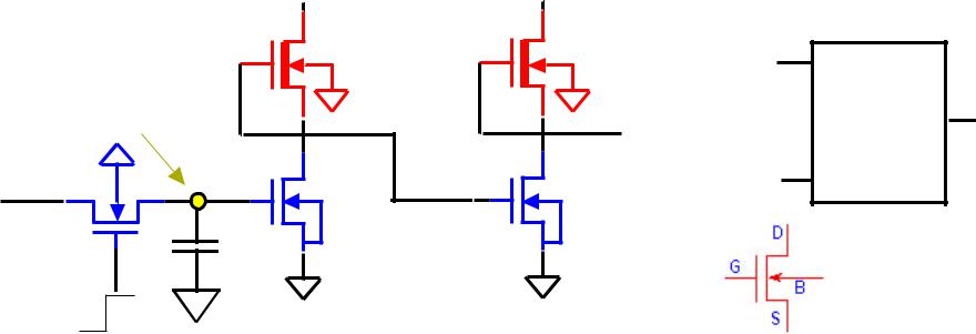
Consider the following depletion nMOS dynamic D-latch circuit:
VDD |
VDD |
||
|
|
|
|
|
M2 |
M4 |
|
D |
|
|
|
|
|
|
|
|
|
|
soft node |
|
|
Q |
D - |
Q |
|
|
|
Latch |
|||
|
Vx |
M1 |
M3 |
|
||
|
|
|
||||
D |
|
CK |
|
|||
|
|
|
|
|
||
MP |
Cx |
Vy |
|
|
|
|
|
|
|
|
|
|
|
|
CK |
|
|
|
|
|
CK = 1: MP turns ON. Cx is charged up or down through MP depending on the input D voltage level. Q = D.
CK = 0: MP turns OFF, and Cx is isolated from input D. Q is determined by charge stored on Cx during previous CK = 1.
Kenneth R. Laker, University of Pennsylvania
VDD
M2 |
soft node
D (V ) |
V |
M1 |
|
x |
|
D |
|
|
MP 
 Cx
Cx
CK 
4
|
|
|
|
|
|
VDD |
(W/L)driver = 2 |
|||||||||||
M4 |
|
|
|
|
|
|
|
|
|
|
|
|||||||
|
|
|
|
|
|
|
|
|
|
|
(W/L)load = 0.5 |
|||||||
|
|
|
|
|
|
|
|
|
|
|
||||||||
|
|
|
|
|
|
|
|
|
|
|
|
|
|
|
|
|
||
|
|
|
|
|
|
|
|
|
|
|
|
|
|
|
|
|
||
|
|
|
|
|
|
|
|
|
|
|
|
|
|
|
|
|
k ’ = 20 |
μA/V2 |
|
|
|
|
|
|
|
|
|
|
|
|
|
|
|
|
|
||
|
|
|
|
|
|
|
|
|
|
|
|
|
|
|
|
Q (V ) |
n |
|
|
|
|
|
|
|
|
|
|
|
|
|
|
|
|
|
|
||
|
|
|
|
|
|
|
|
|
|
|
|
|
|
|
|
V |
= 1.0 V |
|
|
|
|
|
|
|
|
|
|
|
|
|
|
|
|
|
|||
M3 |
|
|
|
|
|
|
|
|
|
|
Q |
T0,driver |
|
|||||
|
|
|
|
|
|
|
|
|
|
|
VT0,load = - 3.0 V |
|||||||
|
|
|
|
|
|
|
|
|
|
|
|
|
|
|
|
|
||
Vy |
|
|
|
|
|
|
|
|
|
|
|
γ = 0.37 V1/2 |
||||||
|
|
|
|
|
|
|
|
|
|
|
||||||||
|
|
|
|
|
|
|
|
|
|
|
|2φF| = 0.6 V |
|||||||
|
|
|
|
|
|
|
|
|
|
|
||||||||
|
|
|
|
|
|
|
|
|
|
|
|
|
|
|
|
|
||
|
|
|
|
|
|
|
|
|
|
|
|
|
|
|
|
|
||
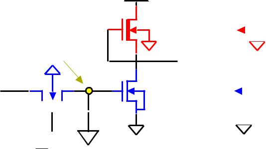
During CK = 1: Let D = 1, i.e. VD = VOH = VDD. MP is conducting and charges Cx to a “weak 1”(i.e. Vx = VDD - VT,driver). M1 is ON: Vy = VOL < VT,driver => M3 is OFF: VQ = VDD or Q = 1.
During CK = 0: Logic-level Vx is preserved through charge storage on Cx. However, Vx starts to drop due to leakage.
WHAT IS THE MINIMUM Vx NEEDED TO KEEP Q = 1 WHEN CK = 0?
Kenneth R. Laker, University of Pennsylvania
VDD |
5 |
|||
VDD |
||||
|
|
|
|
|
M2 |
soft node
D (V ) |
V |
M1 |
|
x |
|
D |
|
|
MP 
 Cx
Cx
CK 
M4 |
|
|
|
|
|
|
|
|
|
|
(W/L)driver = 2 |
|||||
|
|
|
|
|
|
|
|
|
|
|||||||
|
|
|
|
|
|
|
|
|
|
|
|
|
|
|
|
(W/L)load = 0.5 |
|
|
|
|
|
|
|
|
|
|
|
|
|
|
|
|
|
|
|
|
|
|
|
|
|
|
|
|
|
|
|
|
Q (VQ) |
k ’ = 20 μA/V2 |
|
|
|
|
|
|
|
|
|
|
|
|
|
|
|
||
|
|
|
|
|
|
|
|
|
|
|
|
|
|
|
||
|
|
|
|
|
|
|
|
|
|
|
|
|
|
|
n |
|
M3 |
|
|
|
|
|
|
|
|
|
|
VT0,driver = 1.0 V |
|||||
|
|
|
|
|
|
|
|
|
||||||||
|
|
|
|
|
|
|
|
|
|
|
|
|
|
|
|
VT0,load = - 3.0 V |
Vy |
|
|
|
|
|
|
|
|
|
|
||||||
|
|
|
|
|
|
|
|
|
|
γ = 0.37 V1/2 |
||||||
|
|
|
|
|
|
|
|
|
|
|||||||
|
|
|
|
|
|
|
|
|
|
|||||||
|2φF| = 0.6 V
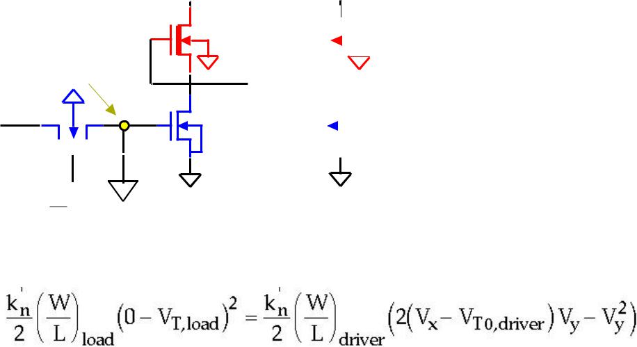
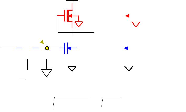
NOTE: for VQ = VDD, M3 must be OFF => Vy = VOL < VT,driver = 1.0 V, i.e. M1 is in LIN region and M2 is in SAT.
|
(20μ A/V2 ) |
(0.5)(0 − V |
)2 = |
|
(20μ A/V2 ) |
(2)(2(V − 1.0V)V − V2 ) |
|
|
|
||||||
2 |
T,load |
|
2 |
x |
y y |
||
|
|
|
|
||||
Assume that Vy = VT0,drive = 1 V, i.e. just small enough to keep M3 OFF
Kenneth R. Laker, University of Pennsylvania
VDD |
6 |
VDD |
M2 |
soft node

 Vx M1
Vx M1 D MP
D MP 


 Cx
Cx 

CK 
M4 |
|
|
|
|
|
|
|
|
|
|
|
(W/L)driver = 2 |
|||||
|
|
|
|
|
|
|
|
|
|
|
|||||||
|
|
|
|
|
|
|
|
|
|
|
|||||||
|
|
|
|
|
|
|
|
|
|
|
(W/L)load = 0.5 |
||||||
|
|
|
|
|
|
|
|
|
|
|
|
|
|
|
|
|
|
|
|
|
|
|
|
|
|
|
|
|
|
|
|
|
|
|
|
|
|
|
|
|
|
|
|
|
|
|
|
|
|
|
|
|
k ’ = 20 μA/V2 |
|
|
|
|
|
|
|
|
|
|
|
|
|
|
|
|
|
|
|
|
|
|
|
|
|
|
|
|
|
|
|
|
|
|
Q |
n |
|
|
|
|
|
|
|
|
|
|
|
|
|
|
|
|
||
|
|
|
|
|
|
|
|
|
|
|
|
|
|
|
|
VT0,driver = 1.0 V |
|
M3 |
|
|
|
|
|
|
|||||||||||
|
|
|
|
||||||||||||||
|
|
|
|
|
|
VT0,load = - 3.0 V |
|||||||||||
|
|
|
|
|
|
|
|
|
|
|
|
|
|
|
|
|
|
|
|
|
|
|
|
|
|
|
|
|
|
|
|
|
|
|
γ = 0.37 V1/2 |
Vy |
|
|
|
|
|
|
|
||||||||||
|
|
|
|
|
|
|2φF| = 0.6 V |
|||||||||||
|
|
|
|
|
|
||||||||||||
|
|
|
|
|
|
|
|
|
|
|
|
|
|
|
|
|
|
|
|
|
|
|
|
|
|
|
|
|
|
|
|
|
|
|
|
Assume that Vy = VT0,drive = 1 V, i.e. just small enough to keep M3 OFF
VT,load = VT0,load+ γ( |2φF |+ Vy −
  |2φF |)
= −3V+ 0.37V1/2 (
 0.6V+ 1.0V −
 0.6V) = -2.84 V Using the current Eq, solve for Vx, i.e.
(0.5)(+2.84)2 = (2)(2(Vx − 1.0V)1.0 − (1.0)2 ) => Vx = 2.51 V
i.e. Vx can drop from VDD to 2.51V due to charge leakage, before VQ is effected (i.e. the output changes state)
Kenneth R. Laker, University of Pennsylvania
7
BASIC PRNCIPLES OF PASS TRANSISTOR CIRCUITS
VDD
M2 |
|
soft node |
|
|
|
|
|
|
|
|
|
|
|
|
|
Vout |
|
|
|
|
|
|
|
|
|
|
|
|
|
|
|
|
|
|
|
|||||||||||||||
|
|
|
|
|
|
|
|
|
|
|
|
|
|
|
|
|
|
|
|
|
|
|
|
|
|
|
|
|
|
|
|
|
|||||||||||||||||
Vin |
|
|
|
|
|
|
|
|
|
|
|
|
|
V |
x |
M1 |
|
|
|
|
|
|
|
|
|
|
|
|
|
|
|
|
|
|
|
|
|
||||||||||||
|
|
|
|
|
|
|
|
|
|
|
|
|
|
|
|
|
|
|
|
|
|
|
|
|
|
|
|
|
|
|
|
|
|
|
|
||||||||||||||
|
|
|
|
|
|
|
|
|
|
|
|
|
|
|
|
|
|
|
|
|
|
|
|
|
|
|
|
|
|
|
|
|
|
|
|
||||||||||||||
|
|
|
|
|
|
|
|
|
|
|
|
|
|
|
|
|
|
|
|
|
|
|
|
|
|
|
|
|
|
|
|
|
|
|
|
|
|
|
|
|
|
|
|
|
|
||||
|
|
|
|
|
|
|
|
|
|
|
|
|
|
|
|
|
|
|
|
|
|
|
|
|
|
|
|
|
|
|
|
|
|
|
|
|
|
|
|
|
|
|
|
|
|
|
|
|
|
MP |
|
|
|
|
|
|
|
|
|
|
|
|
|
|
|
|
|
|
|
|
|
|
|
|
|
|
|
|
|
|
|
|
|
|
|
|
|
|
|
|
|
|
|
|
|
|
|
|
|
|
|
|
|
|
|
|
|
|
|
|
|
|
|
|
|
|
Cx |
|
|
|
|
|
|
|
|
|
|
|
|
|
|
|
|
|
|
|
|
|
|
|
|||||||||
|
|
|
|
|
|
|
|
|
|
|
|
|
|
|
|
|
|
|
|
|
|
|
|
|
|
|
|
|
|
|
|
|
|
|
|
|
|
||||||||||||
|
CK |
|
|
|
|
|
|
|
|
|
|
|
|
|
|
|
|
|
|
|
|
|
|
|
|
|
|
|
|
|
|
|
Vx |
||||||||||||||||
|
|
|
|
|
|
|
|
|
|
|
|
|
|
|
|
|
|
|
|
|
|
|
|
|
|
|
|
|
|
|
|
||||||||||||||||||
|
|
|
|
|
|
|
|
|
|
|
|
|
|
|
|
|
|
|
|
|
|
|
|
|
|
|
|
|
|
|
|
|
|
|
|
|
|
|
|
||||||||||
|
|
|
|
|
|
|
|
|
|
|
|
|
|
|
|
|
|
|
|
|
|
Vin = VDD |
|
|
D |
|
|
|
|
|
|
S |
|||||||||||||||||
|
|
|
|
|
|
|
|
|
|
|
|
|
|
|
|
|
|
|
|
|
|
|
|
|
|
|
|
|
|
||||||||||||||||||||
|
|
|
|
|
|
|
|
|
|
|
|
|
|
|
|
|
|
|
|
|
|
|
|
|
|
|
|
|
|
||||||||||||||||||||
|
|
|
|
|
|
|
|
|
|
|
|
|
|
|
|
|
|
|
|
|
|
|
|
|
|
|
|
|
|
|
|
|
|
|
|||||||||||||||
|
|
|
|
|
|
|
|
|
|
|
|
|
|
|
|
|
|
|
|
|
|
|
|
|
|
|
|
|
|
|
|
|
|
|
|
|
|
|
|
||||||||||
LOGIC “1” TRANSFER: |
|
|
|
|
|
|
|
|
|
|
|
|
|
|
|
|
|
|
|
||||||||||||||||||||||||||||||
|
MP |
|
|
|
|
|
|
|
|
|
|
|
|
|
|
|
|||||||||||||||||||||||||||||||||
|
|
|
|
|
|
|
|
|
ID |
|
|
|
C |
||||||||||||||||||||||||||||||||||||
|
|
|
|
|
|
|
|
|
|
|
|
|
|
|
|||||||||||||||||||||||||||||||||||
|
|
|
|
|
|
|
|
|
|
|
|
|
|
|
|||||||||||||||||||||||||||||||||||
Assume at t = 0: |
|
|
|
|
|
|
|
|
|
|
|
|
|
|
|
|
|
|
|
|
|
|
|
|
|
|
|
|
|
|
|||||||||||||||||||
|
|
|
|
|
|
|
|
|
|
|
|
|
|
|
|
|
|
|
|
|
|
|
|
|
|
|
|
|
|||||||||||||||||||||
|
|
|
|
|
|
|
|
|
|
|
|
|
|
|
|
|
|
|
|
|
|
|
|
|
|
|
|
|
|
|
|
x |
|||||||||||||||||
Vx (t = 0) = 0 V |
|
|
|
|
|
|
|
|
|
|
|
|
|
|
|
|
CK |
|
|
|
|
|
|
|
|
|
|
||||||||||||||||||||||
|
|
|
|
|
|
|
|
|
|
|
|
|
|
|
|
|
|
|
|
|
|
|
|
|
|
||||||||||||||||||||||||
Vin = VOH |
|
|
|
|
|
|
|
|
|
|
|
|
|
|
|
|
|
|
|
|
|
|
|
|
|
|
|
|
|
|
|
|
|
|
|
||||||||||||||
|
|
|
|
|
|
|
|
|
|
|
|
|
|
|
|
|
|
|
|
|
|
|
|
VGS = VDD - Vx, VDS = VDD - Vx |
|||||||||||||||||||||||||
CK = 0 -> VDD |
|
|
|
|
|
|
|
|
|
|
|
|
|
|
|
|
|
|
|
|
|
|
V |
> V |
|
- V => nMOS in SAT |
|||||||||||||||||||||||
|
|
|
|
|
|
|
|
|
|
|
|
|
|
|
|
|
|
|
|
|
|
|
|
|
|
|
|
DS |
|
GS |
|
|
|
T,MP |
|
|
|
|
|
||||||||||
|
C |
|
|
dVx |
= |
kn |
(V − V − V |
)2 |
|
|
|
|
|
|
|
|
|
|
|
|
|
|
|
|
|
||||||||||||||||||||||||
|
|
|
|
|
|
|
|
|
|
|
|
|
|
|
|
|
|
|
|
|
|
||||||||||||||||||||||||||||
|
|
|
|
x |
|
|
dt |
2 |
|
|
|
|
DD |
|
x |
T,MP |
|
|
|
|
|
|
|
|
|
|
|
|
|
|
|
|
|
|
|
||||||||||||||
Kenneth R. Laker, University of Pennsylvania
8
Cx dVdtx = k2n (VDD - Vx - VT,MP )2
Integrating t from 0 -> t and Vx from 0 -> Vx, and neglecting the substrate bias effect i.e.
|
|
2C |
|
|
|
x |
|
|
|
|
|
dV |
|
|
|
|
2C |
|
|
1 |
|
|
ö V |
|||||||||||
t |
|
|
|
|
|
|
|
|
V |
|
|
|
|
|
|
|
|
|
|
|
|
|
|
|
|
|
|
|
|
|
|
|
|
|
ò dt = |
|
|
|
|
x |
|
ò |
|
|
|
|
|
|
x |
|
|
= |
|
|
|
|
|
x |
|
|
|
|
|
|
|
|0 x |
|||
|
k |
|
|
(V |
- V - V |
) |
2 |
|
|
k |
|
|
|
ç |
(V - V - V |
)÷ |
||||||||||||||||||
0 |
|
|
n |
|
|
|
0 |
|
|
|
|
n |
|
|
||||||||||||||||||||
|
|
|
|
|
|
|
|
|
|
|
|
|
DD |
|
x |
T,MP |
|
|
|
|
|
|
|
è |
|
DD |
x |
T,MP ø |
|
|||||
i.e. |
|
|
|
|
|
|
|
|
|
|
|
|
|
|
|
|
|
|
|
|
|
|
|
|
|
|
|
|
|
ö |
|
|
|
|
|
t = |
|
2 C |
|
|
|
|
1 |
|
|
|
|
|
- |
|
|
|
|
1 |
|
|
|
|
|||||||||||
|
|
|
|
|
|
x |
ç |
|
|
|
|
|
|
|
|
|
|
|
÷ |
|
|
|
||||||||||||
|
|
|
k |
n |
|
(V |
|
- V (t) - V |
|
|
) |
(V |
|
- V |
) |
|
|
|
||||||||||||||||
|
|
|
|
|
|
|
|
|
è |
|
DD |
|
x |
T,MP |
|
|
|
|
|
|
DD |
T,MP |
ø |
|
|
|
||||||||
|
|
kn |
(VDD - VT,MP )t |
|
Vx(t) |
|
|
|
|
Vmax = VDD - VT,MP |
|||
Vx (t) = (VDD |
- VT,MP ) |
2Cx |
|
|
|
|
æ k |
|
ö |
|
|||
|
|
|
|
|||
|
|
1 + ç |
n |
(VDD - VT,MP )÷ t |
MP turns OFF |
|
|
|
è 2Cx |
|
ø |
||
|
|
|
|
|
|
when Vx = Vmax |
|
|
|
|
|
|
t |
Kenneth R. Laker, University of Pennsylvania
9
|
|
|
|
kn |
|
(V |
- V |
)t |
||
|
|
|
|
|
|
|
||||
Vx (t) = (VDD |
- VT,MP ) |
|
|
2Cx |
|
|
DD |
T,MP |
|
|
|
|
|
|
|
|
|
||||
|
|
æ k |
n |
|
|
ö |
||||
|
|
|
|
|
|
|||||
|
|
1 + ç |
|
(VDD - VT,MP )÷ t |
||||||
|
|
|
|
|||||||
|
|
|
|
è 2Cx |
|
ø |
||||
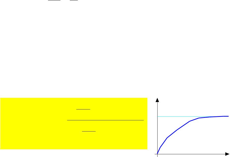
Vmax = Vx(t)|t = ∞ = VDD - VT,MP
Vmax = VDD − VT0,MP− γ( |2φF |+ Vmax −
  |2φF |)
and tcharge = time when Vx = Vmax) |
|
|
|
|
|
||||||
|
2C |
|
1 |
|
1 |
ö |
|||||
tcharge = |
|
x |
ç |
|
|
|
|
- |
|
|
÷ |
k |
|
(V |
- V |
- V |
) |
(V - V |
) |
||||
|
|
n è |
DD |
max |
T,MP |
|
|
DD T,MP |
ø |
||
Body Effect: Reduces Vx and Increases tcharge
Kenneth R. Laker, University of Pennsylvania
SOME PROPERTIES OF PASS TRANSISTOR LOGIC CIRCUITS |
10 |
Propogation of logic “1” in Pass Transistor Strings (impact of weak “1” propogation)
1. Cascade of Pass Transistors
|
VDD |
|
VDD |
VDD |
V |
|||||||||||||||
VDD |
|
|
|
V1 |
|
|
|
V2 |
|
|
V3 |
|
|
|
DD |
|||||
|
|
|
|
|
|
|
|
|
|
|||||||||||
|
|
|
|
|
|
|
|
|
|
|
|
|
Vo |
|||||||
|
|
|
|
|
|
|
|
|
|
|
|
|
||||||||
|
|
|
|
|
|
|
|
|
|
|
|
|||||||||
|
|
|
|
|
|
|
|
|
|
|
|
|
|
|
|
|
|
|
||
M1 |
|
|
M2 M3 |
|
|
|
|
|
||||||||||||
|
|
|
MN |
|||||||||||||||||
At t = 0: Vin = VDD
V1 = V2 = V3 = .. Vo = 0
Pass Transistor Logic
1.Very efficient in use of transistors.
2.Potentially very efficient layouts result.
3.Pass transistors can usually be minimum size devices.
4.Usually more internal node capacitance than with conventional CMOS gates.
Vmax1 = VDD |
- VTn1 |
5. |
Propogation delays can become large in long series |
||||||||||||||||||||||
|
strings of pass transistors. |
||||||||||||||||||||||||
Vmax2 = VDD |
- VTn2 |
|
|||||||||||||||||||||||
6. |
Use of CMOS transmission gates circumvents the VTn |
||||||||||||||||||||||||
|
Vmaxo = VDD |
- VTnN |
|
voltage drop of nMOS pass-transistors. It also doubles |
|||||||||||||||||||||
|
|
the area and interconnects. |
|||||||||||||||||||||||
|
|
|
|
|
|
|
|
|
|
|
|
|
|
|
|
|
|
|
|
|
|
||||
2. Daisy Chain of Pass Transistors |
7. |
Static power dissipation is uneffected. |
|||||||||||||||||||||||
|
|
|
V |
|
|
|
|
|
|
|
|
|
|
|
|
8. |
Dynamic power dissipation may be decreased. |
||||||||
Vi = VDD |
|
|
DD V - V |
|
|
|
|
|
|||||||||||||||||
|
|
|
|
|
|
|
|||||||||||||||||||
|
|
|
|
|
|
DD Tn1 |
|
|
|
|
|
||||||||||||||
|
|
|
|
|
|
|
|
||||||||||||||||||
|
|
|
|
|
|
|
|
|
|
|
|
|
VDD - 2VTn2 |
|
|
|
|
|
|||||||
|
|
M1 |
|
|
|
|
|
|
|
|
|
|
|
Substrate bias different |
|||||||||||
|
|
|
|
|
|
|
|
|
|
|
|
|
|||||||||||||
|
|
|
|
|
|
|
|
|
|
|
|
|
|
||||||||||||
|
|
|
|
|
|
|
|
|
|
|
|
|
|
||||||||||||
|
|
|
|
|
|
|
|
|
|
|
|
|
|
|
|
|
V - 3V |
||||||||
|
|
VDD |
M2 |
|
|
|
|
||||||||||||||||||
|
|
|
|
|
|
for each pass transistor |
|||||||||||||||||||
|
|
|
|
|
|
|
DD Tn3 |
||||||||||||||||||
|
|
|
|
|
|
||||||||||||||||||||
|
|
|
|
|
|
|
|
|
|
|
|
|
|
|
|
|
|||||||||
|
|
|
|
|
|
VDD M3 |
|
|
|
|
|||||||||||||||
|
TO BE AVOIDED! |
|
|
|
|
|
Vo = VDD - NVTnN |
||||||||||||||||||
|
|
|
|
|
|
||||||||||||||||||||
|
|
|
|
|
|
|
|
|
|
|
|
|
|
|
|
|
V |
|
|
|
|
|
|
||
|
|
|
|
|
|
|
|
|
|
|
|
|
|
|
|
|
|
DD MN |
|
|
|
||||
Kenneth R. Laker, University of Pennsylvania |
|
|
|
|
|
||||||||||||||||||||