

31
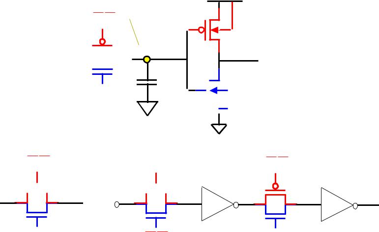
DYNAMIC CMOS TRANSMISSION GATE LOGIC
|
φ1 |
|
|
φ2 |
|
A |
φ1 |
|
STAGE 1 |
||
|
||
|
STAGE 2 |
B
 F1
F1
C
D
φ1
φ1 |
φ2 |
|
Kenneth R. Laker, University of Pennsylvania
32
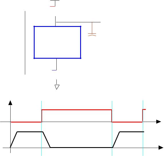
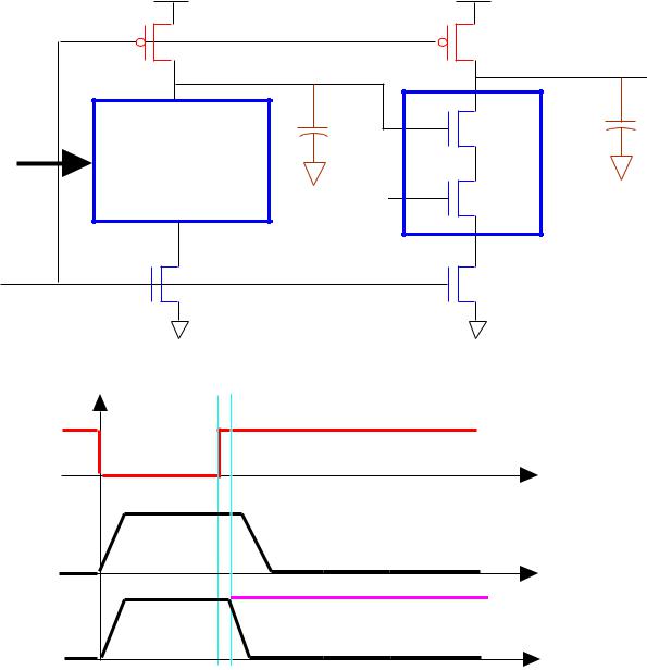
CMOS TRANSMISSION GATE DYNAMIC SHIFT REGISTER
soft node
CK
Vin 


 Vx
Vx
CK Cx
CK CK V1 
 V2
V2 
CK CK
VDD
M2
Vout


 M1
M1
|
CK |
V3 |
V |
|
4 |
CK
Kenneth R. Laker, University of Pennsylvania
33
DYNAMIC CMOS PRECHARGE - EVALUATE LOGIC
VDD


 Mp
Mp
Z
nMOS C inputs Logic
Logic 
Block C-internal capacitance
CK 

 Me
Me
CK = 0 -> C precharges to VDD (output is unavailable during
precharge)
CK = 1 -> C is selectively discharges to 0
(output is only available after discharge is complete)
CK |
1 |
evaluate |
|
||
|
|
|
Z |
precharge |
t |
precharge |
||
|
|
t |
Kenneth R. Laker, University of Pennsylvania
34
VDD
|
Z |
A |
C |
B |
|
C |
|
D |
|
E |
|
CK |
|
Z = A.(B + C) +(D.E) when CK = 1
Z = HIGH when CK = 0
Kenneth R. Laker, University of Pennsylvania
35
|
ADVANTAGES/DISADVANTAGES |
|
|
|
VDD |
|
|
|
|
|
|||||||
1. |
Requires N +2 transistors to realize an N-input gate. |
|
|
|
|
|
|
|
|
||||||||
|
|
|
|
|
|
|
|
|
|
|
|
|
|
|
|
||
2. |
Low static power dissipation. |
|
|
|
|
|
|
|
|
|
Mp |
|
|
Z |
|||
|
|
|
|
|
|
|
|
|
|
|
|||||||
|
|
|
|
|
|
|
|
|
|
|
|||||||
3. |
No dc current paths to place constraints on device sizing. |
|
|
|
|
|
|
|
|
|
|
|
|||||
|
|
|
|
|
|
|
|
|
|
|
|
|
|
||||
4. |
Input capacitance same as pseudo nMOS gate. |
inputs |
|
|
nMOS |
|
|
|
C |
||||||||
|
|
|
|
|
|||||||||||||
|
|
Logic |
|
|
|
||||||||||||
5. |
Pull-up time is improved by active switch to VDD. |
|
|
|
|
|
|
|
|
|
|||||||
|
|
|
|
Block |
|
|
|
|
|
||||||||
1. |
Output is available ≤ 50 % of the time. |
CK |
|
|
|
|
|
|
|
|
Me |
|
|
|
|
|
|
|
|
|
|
|
|
|
|
|
|
|
|
||||||
|
|
|
|
|
|
|
|
|
|
|
|
|
|
|
|
|
|
2.Pull-down time is degraded due to series active switch to 0.
3.Logic output value can be degraded due to charge sharing with other gate capacitances connecte to the output.
4.Minimum clock rate determined by leakage on C.
5.Maximum clock rate determined by circuit delays.
6.Inputs can only change during the precharge phase. Inputs must be stable during evaluation; otherwise an incorrect value on an input could erroneously discharge the output node.
(single phase P-E logic gates can not be cascaded)
7.Outputs must be stored during precharge, if they are required during the next evaluate phase.
Kenneth R. Laker, University of Pennsylvania
|
|
|
|
36 |
|
VDD |
VDD |
|
|
|
Mp1 |
Mp2 |
|
Vout2 |
|
|
Vout1 |
|
|
|
|
|
|
|
inputs |
nMOS |
C |
|
C |
Logic |
1 |
|
|
|
|
Block1 |
nMOS |
||
CK |
|
|
Logic |
|
M |
Me2 |
Block2 |
||
|
|
|
||
|
e1 |
|
|
|
|
precharge |
evaluate |
|
|
|
CK |
|
|
|
|
1 |
|
|
|
|
Vout1 |
|
t |
|
|
|
|
evaluate: |
|
|
|
|
t |
|
|
Vout2 |
correct state |
Me1, Me2 -> ON |
|
|
erroneous state |
|
Mp1, Mp2 -> OFF |
|
|
|
t |
||
|
|
|
||
|
|
|
|
|
Kenneth R. Laker, University of Pennsylvania
37
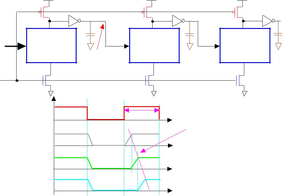
HIGH PERFORMANCE DYNAMIC CMOS CIRCUITS
DOMINO CMOS LOGIC |
|
|
|
|
|
|
|
|
|
|
|
static inverter serves to |
||||||||||||||||||||||
|
|
|
|
|
|
|
|
|
|
VDD |
|
|
|
|
|
|
VDD |
|||||||||||||||||
|
|
|
|
|
|
|
|
|
|
|
|
|
|
|
|
buffer the logic part of the |
||||||||||||||||||
|
|
|
|
|
|
|
|
|
|
|
|
|
|
|
|
|
|
|
|
PZ |
|
|
|
|
|
|
|
circuit from its output load |
||||||
|
|
|
|
|
|
|
|
|
|
|
|
|
|
|
|
|
|
|
|
|
|
|
|
|
|
|
||||||||
|
|
|
|
|
|
|
|
|
|
|
|
|
|
|
|
|
|
|
|
|
|
|
|
|
|
|
||||||||
|
|
|
|
|
|
|
|
|
|
|
|
|
|
|
|
|
|
|
|
|
|
|
|
|
|
|
||||||||
|
|
|
|
|
|
|
|
|
|
|
|
|
|
|
|
|
|
|
|
|
|
|
|
|
|
|
|
|
|
Z |
||||
|
|
|
|
|
|
|
|
|
|
|
|
|
|
|
|
|
|
|
|
|
|
|
|
|
|
|
|
|
||||||
|
|
|
|
|
|
|
|
|
|
|
|
|
|
|
|
|
|
|
|
|
|
|
||||||||||||
|
|
|
|
|
|
|
|
|
|
|
|
|
|
|
|
|
|
|
|
|
|
|
|
|
|
|
|
|
|
|
|
|
|
|
|
|
|
|
|
|
|
|
|
|
|
|
|
|
|
|
|
|
|
|
|
|
|
|
|
|
|
|
|
|
|
|
|
|
|
|
|
|
|
|
|
|
|
nMOS |
|
|
|
|
|
|
|
|
|
|
|
|
|
|
|
|||||||||||
inputs |
|
|
|
|
|
|
|
C |
|
|
|
|
|
|
|
CL |
||||||||||||||||||
|
|
|
|
|
|
|
|
|
|
|
|
|
|
|||||||||||||||||||||
|
|
|
|
|
Logic |
|
|
|
|
|
|
|
|
|
||||||||||||||||||||
|
|
|
|
|
|
|
|
|
|
|
|
|
|
|
|
|||||||||||||||||||
|
|
|
|
|
|
|
|
|
|
|
|
|
|
|
|
|
|
|
|
|||||||||||||||
|
|
|
|
|
|
|
|
|
Block |
|
can also be pMOS |
|||||||||||||||||||||||
|
|
|
|
|
|
|
|
|
|
|
|
|
|
|
|
|
|
|
|
|
||||||||||||||
|
|
CK |
|
|
|
|
|
|
|
|
|
|
|
|
|
|
|
|
|
|
logic block |
|
|
|
|
|||||||||
|
|
|
|
|
|
|
|
|
|
|
|
|
|
|
|
|
|
CK = 0 -> C precharges to VDD, Z = 0. |
||||||||||||||||
|
|
|
|
|
|
|
|
|
|
|
|
|
|
|
|
|||||||||||||||||||
|
|
|
|
|
|
|
|
|
|
|
|
|
|
|
|
|
|
|
|
|||||||||||||||
|
|
|
|
|
|
|
|
|
|
|
|
|
|
|
|
|
|
|
|
|||||||||||||||
|
|
CK |
|
|
|
|
|
|
|
|
|
|
|
|
|
|
(output is unavailable during precharge) |
|||||||||||||||||
|
|
|
|
|
|
|
|
|
|
|
|
|
|
|
|
CK = 1 -> C is selectively discharges to 0, |
||||||||||||||||||
|
1 |
|
|
|
|
|
|
|
|
|
|
|
|
|
|
|
||||||||||||||||||
|
|
|
|
|
|
|
|
|
|
|
|
|
|
|
|
|||||||||||||||||||
|
|
|
evaluate |
|
Z selectively charges to 1. |
|||||||||||||||||||||||||||||
|
|
|
|
|
|
|
|
|
|
|
|
|
|
|
|
|
|
|
t |
|||||||||||||||
|
precharge |
|
|
|
|
|
|
|
|
|
|
|
(output is only available after node Z |
|||||||||||||||||||||
|
|
|
|
|
|
|
|
|
|
|
|
|
||||||||||||||||||||||
|
|
|
|
|
|
|
|
|
|
|
|
|
|
|
|
|
|
|
|
|||||||||||||||
|
|
|
|
|
|
|
|
|
|
|
|
|
|
|
|
|
|
|
|
charge is complete) |
||||||||||||||
Kenneth R. Laker, University of Pennsylvania
|
|
|
|
38 |
|
VDD |
VDD |
|
VDD |
|
|
O1 |
O2 |
O3 |
|
|
|
||
inputs |
nMOS- |
nMOS- |
|
nMOS- |
Logic |
Logic |
|
Logic |
|
|
Block 1 |
precharged Block 2 |
|
Block 3 |
|
|
to 0 |
|
|
CK |
|
|
|
|
evaluate |
evaluate |
|
|
CK |
teval |
|
|
precharge |
t |
||
|
|||
|
|
||
O1 |
|
|
|
O2 |
|
t |
|
|
|
||
|
|
t |
|
O3 |
|
t |
|
|
|
propogating gate decisions
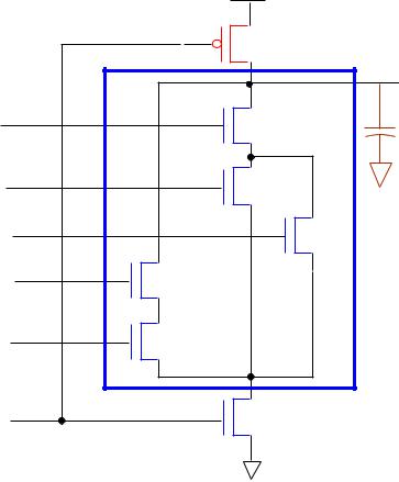
Max # stages limited: total prop delay < teval.
Kenneth R. Laker, University of Pennsylvania
39
weak pull-up (small kp, i.e. large L/W) pMOS transistor used maintain a precharged high if the clock were to stop. Weakened so that it does not interfere with pull-down
VDD |
|
|
|
|
|
|
|
VDD |
|
|
|
|||||||||||
|
|
|
|
|
|
|
|
|
|
|
|
|
|
|
|
|
|
|
|
|
|
|
|
|
|
|
|
|
|
|
|
|
|
|
|
|
|
|
|
|
|
|
|
|
|
|
|
|
|
|
|
|
|
|
|
|
|
|
|
|
|
|
|
|
|
|
|
|
|
|
|
|
|
|
|
|
|
|
|
|
|
|
|
|
|
|
|
|
|
|
|
|
|
|
|
|
|
|
|
|
|
|
|
|
|
|
|
|
|
|
|
|
|
|
|
|
|
|
|
|
|
|
|
|
|
|
|
|
|
|
|
|
|
|
|
|
|
|
|
|
|
|
|
|
|
|
|
|
|
|
|
|
|
|
|
|
|
|
|
|
|
|
|
|
|
|
|
|
|
|
|
|
|
|
|
|
|
|
|
|
|
|
|
|
|
nMOS |
|
|
|
|
|
|
|
nMOS |
||||||||
|
|
|
|
|
|
|
|
|
|
|
||||||||||
|
|
|
|
|
|
|
|
|
|
|
||||||||||
inputs |
|
|
Logic |
|
|
|
inputs |
|
|
Logic |
||||||||||
|
|
|
|
|
||||||||||||||||
|
|
|
|
|
|
|||||||||||||||
|
|
|
|
Block |
|
|
|
|
|
|
|
Block |
||||||||
CK |
|
|
|
|
|
|
|
|
|
CK |
|
|
|
|
|
|
||||
|
|
|
|
|
|
|
|
|
|
|||||||||||
|
|
|
|
|
|
|
|
|
|
|
|
|||||||||
|
|
|
|
|
|
|
|
|
|
|
|
|
|
|
|
|
|
|
|
|
Kenneth R. Laker, University of Pennsylvania
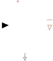
40
CHARGE SHARING BETWEEN OUTPUT CAPACITANCE C1 AND
INTERMEDIATE NODE CAPACITANCE C2 DURING
|
|
|
|
|
|
|
|
|
|
|
EVALUATION |
|
|
|
|
|
|
|
|
|
|
|
|
|
|
|
|
|
|||||||||||||||||||
|
|
|
|
|
|
|
|
|
|
|
|
|
|
VDD |
|
|
|
V |
|
|
|
|
|
|
|||||||||||||||||||||||
|
|
|
|
|
|
|
|
|
|
|
|
|
|
|
|
|
|
|
|
|
|
|
|
|
|
|
Vx |
|
|
|
|
|
|
DD |
Z |
|
|
|
|
||||||||
|
|
|
|
|
|
|
|
|
|
|
|
|
|
|
|
|
|
|
|
|
|
|
|
|
|
|
|
|
|
|
|||||||||||||||||
|
|
|
|
|
|
|
|
|
|
|
|
|
|
|
|
|
|
|
|
|
|
|
|
|
|
|
|
|
|
|
|
|
|
|
|
|
|
|
|
|
|
||||||
|
|
|
|
|
|
|
|
|
|
|
|
|
|
|
|
|
|
|
|
|
|
|
|
|
|
|
|
|
|
|
|
|
|
|
|
|
|
|
|
|
|
||||||
|
|
|
|
|
|
|
|
|
|
|
|
|
|
|
|
|
|
|
|
|
|
|
|
|
|
|
|
|
|
|
|
|
|
|
|
|
|
|
|
|
|
||||||
|
|
|
|
|
|
|
|
|
|
|
|
|
|
|
|
|
|
|
|
|
|
|
|
|
|
|
|
|
|
|
|
|
|
|
|
|
|
|
|
|
|
||||||
|
|
|
|
|
|
|
|
|
|
|
|
|
|
|
|
|
|
|
|
|
|
|
|
|
|
|
|
|
|
|
|
|
|
|
|
|
|
|
|
|
|
||||||
|
|
|
|
|
|
|
|
|
|
|
|
|
|
|
|
|
|
|
|
|
|
|
|
|
|
|
|
|
|
|
|
|
|
|
|
|
|
|
|
|
|
||||||
|
|
|
|
|
|
|
|
|
|
|
|
|
|
|
|
|
|
|
|
|
|
|
|
|
|
|
|
|
|
|
|
|
|
|
|
|
|
|
|
|
|
|
|
|
|
||
|
|
|
|
|
|
|
|
|
|
|
|
|
|
|
|
|
|
|
|
|
|
|
|
|
|
|
|
|
|
|
|
|
|
|
|
|
|
|
|
|
|
|
|
|
|
|
|
|
|
|
|
|
|
|
|
|
|
|
|
|
|
|
|
|
|
|
|
|
|
|
|
|
|
|
|
|
|
|
|
|
|
|
|
|
|
|
|
|
|
|
|
|
|
|
|
|
|
|
|
|
|
|
|
|
|
|
|
|
|
|
|
|
|
N1 |
|
|
|
|
C1 |
|
|
|
|
|
|
|
|
|
|
|
|
|
|
||||||||||
|
|
|
|
|
|
|
|
|
|
|
|
|
|
|
|
|
|
|
|
|
|
|
|
|
|
|
|
|
|
|
Vx |
= |
|
VDDC1 |
|||||||||||||
|
|
|
|
|
|
|
|
|
|
|
|
|
|
|
|
|
|
|
|
|
|
|
|
|
|
|
|
|
|
|
|
||||||||||||||||
|
|
|
|
|
|
|
|
|
|
|
|
|
|
|
|
|
|
|
|
|
|
|
|
|
|
|
|
|
|
|
|||||||||||||||||
|
|
|
|
|
|
|
|
|
|
|
|
|
|
|
|
|
|
|
|
|
|
|
|
|
|
|
|
|
|
|
|
|
|
|
|
|
|
|
|
||||||||
|
|
|
|
|
|
|
|
|
|
|
|
|
|
|
|
|
|
|
|
|
|
|
|
|
|
|
|
|
|
|
|
|
|
|
|
|
|
|
|
|
|
|
|
||||
|
|
|
|
|
|
|
|
|
|
|
|
|
|
|
|
|
|
|
|
|
|
|
|
|
|
|
|
|
|
|
|
|
|
|
|
|
|
|
|
|
|
|
|
|
|
||
|
|
|
|
|
|
|
|
|
|
|
|
|
|
|
|
|
|
|
|
|
|
|
|
|
|
|
|
|
|
|
|
|
|
|
|
|
|
|
|
|
|
|
|
|
|
C1 + C2 |
|
|
|
|
|
|
|
|
|
|
|
|
|
|
|
|
|
|
|
|
|
|
|
|
|
|
|
|
|
|
|
|
|
|
|
|
|
|
|
|
|
|
|
|
|
|
|||
|
|
inputs |
|
|
|
|
|
|
|
|
|
|
|
|
|
|
|
|
|
|
C2 |
|
|
|
|
|
|
|
|
|
|
|
|
|
|
|
|
|
|
||||||||
|
|
|
|
|
|
|
|
|
|
|
|
|
|
|
|
|
|
|
|
|
|
|
|
|
|
|
|
|
|
|
|
|
|
|
|
|
|
||||||||||
|
|
|
|
|
|
|
|
|
|
|
|
|
|
|
|
|
|
|
|
|
|
|
|
|
|
|
|
|
|
|
|
|
|
|
|
|
|
||||||||||
|
|
|
|
|
|
|
|
|
|
|
|
|
|
|
|
|
|
|
|
|
|
|
|
|
|
|
|
|
|
|
|
|
|
|
|
|
|
||||||||||
CK |
|
|
|
|
|
|
|
|
|
|
|
|
|
|
|
|
|
|
|
|
|
|
|
|
|
|
|
|
|
|
|
|
|
|
|
|
|
|
|
|
KEEP C2 << C1 |
||||||
|
|
|
|
|
|
|
|
|
|
|
|
|
|
|
|
|
|
|
|
|
|
|
|
|
|
|
|
|
|
|
|
|
|
|
|
|
|
|
|
|
|
||||||
|
|
|
|
|
|
|
|
|
|
|
|
|
|
|
|
|
|
|
|
|
|
|
|
|
|
|
|
|
|
|
|
|
|
|
|
|
|
|
|
|
|
||||||
|
|
|
|
|
|
|
|
|
|
|
|
|
|
|
|
|
|
|
|
nMOS Logic Block |
|
||||||||||||||||||||||||||
|
|
|
|
|
|
|
|
|
|
|
|
|
|
|
|
|
|
|
|
|
|
|
|
|
|
||||||||||||||||||||||
|
|
|
|
|
|
|
|
|
|
|
|
|
|
|
|
|
|
|
|
|
|
|
|
|
|||||||||||||||||||||||
|
|
|
|
|
|
|
|
|
|
|
|
|
|
|
|
|
|
|
|
|
|
|
|
||||||||||||||||||||||||
|
|
|
|
|
|
|
|
|
|
|
|
|
|
|
|
|
|
|
|
|
|
|
|
|
|||||||||||||||||||||||
|
|
|
|
|
|
|
|
|
|
|
|
|
|
|
|
|
|
|
|
|
|
|
|
|
|
|
|
|
|
|
|
|
|
|
|
|
|
|
|
|
|
|
|
|
|
|
|
1.Assume initially that all inputs are 0V and voltage across C2 is at 0V.
2.During pre-charge, i.e. CK = 0, C1 is charged to VDD.
3.If the input to N1 switches from 0 to 1 during the evaluation phase, i.e.
CK = 1, charge initially stored on C1 will be shared with C2; thus, reducing the value of Vx.
Kenneth R. Laker, University of Pennsylvania