

41
REDUCE CHARGE SHARING DEGRADATION OF Vx
WEAK PULLUP
|
|
|
|
|
|
|
|
|
|
|
VDD |
|
|
weak pullup pMOS |
||||||||||||
|
|
|
|
|
|
|
|
|
|
|
|
|
|
|
|
|
|
|
||||||||
|
|
|
|
|
|
|
|
|
|
|
|
|
|
|
|
|
|
|
||||||||
|
|
|
|
|
|
|
|
|
|
|
|
|
|
|
|
|
|
|
|
|
|
|
|
|
|
|
|
|
|
|
|
V |
|
|
|
|
|
|
|
|
|
|
|
|
|
|
|
|
|
|
|
V |
|
|
|
|
|
|
x |
|
|
|
|
|
|
|
|
|
|
|
|
|
|
|
|
|||||
|
|
|
|
|
|
|
|
|
|
|
|
|
|
|
|
|
|
|
|
|
||||||
|
|
|
|
|
|
|
|
|
|
|
|
|
|
|
|
|
|
|
|
|
|
|
|
|
|
out |
|
|
|
|
|
|
|
|
|
|
|
|
|
|
|
|
|
|
|
|
|
|
|
|
|
||
|
|
|
|
|
|
nMOS |
|
|
|
|
|
|
|
|
|
Pushes Vx to VDD unless there |
||||||||||
inputs |
|
|
|
|
Logic |
|
|
|
|
|
|
|
|
|
||||||||||||
|
|
|
|
|
|
|
|
|
|
|
|
|
is a strong pull-down path |
|||||||||||||
|
|
|
|
|
|
|
||||||||||||||||||||
|
|
|
|
|
|
Block |
|
|
|
|
|
|
|
|
|
between Vout and ground. |
||||||||||
CK |
|
|
|
|
|
|
|
|
|
|
|
|
|
|
|
|
|
|
|
|
|
|
|
|
||
|
|
|
|
|
|
|
|
|
|
|
|
|
|
|
|
|
|
|
|
|
|
|||||
|
|
|
|
|
|
|
|
|
|
|
|
|
|
|
|
|
|
|
|
|
|
|
|
|||
|
|
|
|
|
|
|
|
|
|
|
|
|
|
|
|
|
|
|
|
|
|
|
|
|
|
|
Kenneth R. Laker, University of Pennsylvania
42
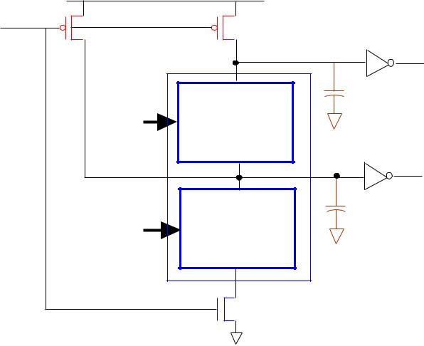
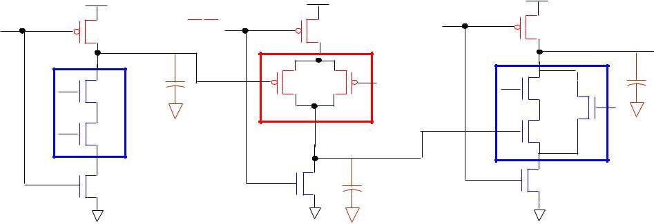
SEPERATE pMOS TRANSISTORS TO PRECHARGE INTERMEDIATE HIGH CAPACITANCE NODES
VDD |
|
|
|
CK |
|
Vx1 |
|
|
|
Vout1 |
|
|
|
|
|
inputs |
nMOS |
C1 |
|
|
Logic |
|
|
|
Sub-Block |
Vx2 |
Vout2 |
inputs |
nMOS |
|
|
C2 |
|
||
Logic |
|
||
|
|
|
|
|
Sub-Block |
|
|
|
nMOS Logic Block |
||
EFFECTIVELY ELIMINATES ALL CHARGE SHARING PROBLEMS
DURING EVALUATION
Kenneth R. Laker, University of Pennsylvania
|
|
VDD |
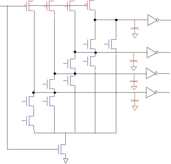
43 |
||
|
|
|
|
|
|
|
|
|
|
|
|
CK
|
C4 |
|
P4 |
G4 |
|
P3 |
C3 |
|
|
||
G3 |
C2 |
|
P2 |
||
|
||
G2 |
C1 |
|
P1 |
||
|
||
G1 |
|
|
C0 |
|
C1 = G1 + P1*C0
C2 = G2 + P2*G1 + P2*P1*C0
C3 = G3 + P3*G2 + P3*P2*G1 + P3*P2*P1*C0
C4 = G4 + P4*G3 + P4*P3*G2 + P4*P3*P2*G1 + P4*P3*P2*P1*C0
Kenneth R. Laker, University of Pennsylvania
VDD
VA
VB = 0
CK
44
Vx1 = 0 at t = 0
Vout
 C1
C1
Let C1 = C2 = 0.05 pF
Vx2 = 0 at t = 0
 C2
C2
nMOS Logic Block
WITHOUT |
|
|
|
|
|
|
VDDC1 |
|
VDD |
|
|||
|
|
|
|
|
|
|
|
||||||
|
|
|
|
|
|
|
V |
¹ V |
EVALUATION:V = |
= |
|
||
PRECHARGE: |
|
||||||||||||
|
|
|
|||||||||||
x1 |
x 2 |
x1 |
C1 + C2 |
2 |
|
||||||||
WITH |
|
|
|
|
|
|
|
|
|
|
|||
|
|
|
|
|
|
|
|
|
|
||||
|
|
|
|
PRECHARGE: Vx1 = Vx2 EVALUATION: Vx1 = VDD |
|||||||||
|
|
|
|
|
|||||||||
|
|
|
|
|
|
||||||||
|
|
|
|
|
|
|
|
|
|
|
|
|
|
Kenneth R. Laker, University of Pennsylvania
45
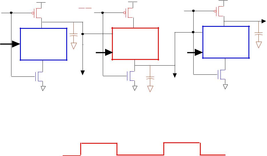
NP DOMINO LOGIC (NORA or ZIPPER CMOS)
|
V |
VDD |
|
|
|
DD |
|
|
|
CK |
|
CK |
CK |
|
inputs |
nMOS |
pMOS |
|
|
logic |
inputs logic |
inputs |
||
|
||||
|
block |
block |
|
To other |
To other |
pMOS |
nMOS |
blocks |
blocks |
VDD To other
pMOS blocks
nMOS logic block
NOTE: INVERTERS ARE NOT REQUIRED AT OUTPUTS OF STAGES
ALL inputs stable when CK = 1
CK
nMOS stages
all stages precharge all stages evaluate pMOS stagesevaluate
pre-discharge
Kenneth R. Laker, University of Pennsylvania
46
NP DOMINO LOGIC (NORA or ZIPPER CMOS) EXAMPLE
|
V |
VDD |
VDD |
|
DD |
|
|
CK |
CK |
|
CK |
Kenneth R. Laker, University of Pennsylvania
47
SINGLE PHASE CLOCK PIPELINED DYNAMIC CMOS STRUCTURE
|
V |
VDD |
VDD |
VDD |
|
DD |
|
|
|
CK |
|
CK |
|
|
|
|
|
|
|
inputs |
nMOS |
|
pMOS |
CK |
|
logic |
inputs |
logic |
|
|
block |
CK |
block |
To Next |
|
|
|
|
|
|
|
|
|
nMOS |
|
|
|
|
block |
N-BLOCK |
P-BLOCK |
USING TRISTATE INVERTERS BETWEEN STAGES DECOUPLES THE STAGES AND ENABLES PIPILINED OPERATION.
CK - LOW: nMOS Blocks Precharge to VDD
pMOS Blocks Evaluate by selective pullup to VDD CK-HIGH: pMOS Blocks Pre-discharge to 0V
nMOS Blocks Evaluate by selective pull down to 0V Since CK-Inverse is not used, no clock skew problem can arise. PROVIDES SIMILAR PERFROMANCE TO NORA STRUCTURE.
Kenneth R. Laker, University of Pennsylvania
48
COMMON ADVANTAGES OF DYNAMIC LOGIC STYLES
1.Smaller area than fully static gates.
2.Smaller parasitic capacitances, hence higher speed.
3.Glitch free operation if DESIGNED CARFULLY.
Kenneth R. Laker, University of Pennsylvania
SUMMARY - GUIDELINES |
49 |
|
1.Full complementary static logic is best option in the majority of CMOS
circuits. Noise-immunity not sensitive to kn/kp; does not involve pre charging of nodes; dissipates no DC power; layout can be automated. Large fan-in gates lead to complex circuit structures (2N transistors); larger parasitics; slower and higher dynamic power dissipation than alternatives; no clock.
2.Pseudo-nMOS static logic finds widest utility in large fan-in NOR gates. Requires only N+1 transistors for N fan-in; smaller parasitics; faster and lower dynamic power dissipation than full COS. Noise-immunity sensitive
to kn/kp; dissipates DC power when pulled down; and not well suited for automated layout; no clock.
4. CMOS domino logic should be used for low-power, high speed applications. Requires N+k transistors for N fan-in, size advantages of psuedo-nMOS; dissipates no DC power; noise immunity not sensitive to kn/kp; use of clocks enables synchronous operation. Relies on storage on soft nodes; will require exhaustive simulation at all the process corners to insure proper operation; some of the speed advantage over static gates is diminished by the required pre-charge (pre-discharge) time.
Kenneth R. Laker, University of Pennsylvania