

Process Technology:
Silterra 0.18 m
Features
•Precise Optimization for Silterra’s Six-Layer Metal 0.18 m CMOS Process
•High Density (area is 0.025mm2 )
•Fast Access Time (1.09ns at typical process, 1.80V, 25˚C)
•Fast Cycle Time (1.04ns at typical process, 1.80V, 25˚C)
•One Read/Write Port
•Completely Static Operation
•Near-Zero Hold Time (Data, Address, and Control Inputs)
High-Speed Single-Port Synchronous
SRAM
RAM64x8
64X8, Mux 4, Drive 12
Memory Description
The 64X8 SRAM is a high-performance, synchronous single-port, 64-word by 8-bit memory designed to
take full advantage of Silterra’s six-layer metal, 0.18 m CMOS process.
The SRAM’s storage array is composed of six-transistor cells with fully static memory circuitry. The SRAM operates at a voltage of 1.8V ± 10% and a junction temperature range of 0˚C to +125˚C.
Pin Description
|
Pin |
|
|
|
Description |
|
||
|
|
|
|
|
|
|
|
|
|
A[5:0] |
|
|
Addresses (A[0] = LSB) |
||||
|
|
|
|
|
|
|
|
|
|
D[7:0] |
|
|
Data Inputs (D[0] = LSB) |
||||
|
|
|
|
|
|
|
|
|
|
CLK |
|
|
|
Clock Input |
|
||
|
|
|
|
|
|
|
|
|
|
CEN |
|
|
|
Chip Enable |
|
||
|
|
|
|
|
|
|
|
|
|
WEN |
|
|
|
Write Enable |
|
||
|
|
|
|
|
|
|
|
|
|
OEN |
|
|
|
Output Enable |
|||
|
|
|
|
|
|
|
||
|
Q[7:0] |
|
Data Outputs (Q[0] = LSB) |
|||||
|
|
|
|
|
|
|
|
|
|
Area |
|
|
|
|
|
|
|
|
|
|
|
|
|
|
|
|
|
Area Type |
|
Width (mm) |
|
Height (mm) |
|
Area (mm2) |
|
|
Core |
|
0.141 |
|
0.177 |
|
0.025 |
|
|
|
|
|
|
|
|
|
|
|
Footprint |
|
0.183 |
|
0.220 |
|
0.040 |
|
|
|
|
|
|
|
|
|
|
The footprint area includes the core area and userdefined power ring and pin spacing areas.
Symbol
A[5:0] |
6 |
8 |
Q[7:0] |
|
|
8
D[7:0]
CLK
CEN
WEN
OEN
Silterra Malaysia 0.18um Process SRAM-SP-HS Datasheet, Version 2003Q3V1
Copyright 1997-2003 Artisan Components, Inc.
RAM64x8
SRAM Block Diagram
Model Row
Core
PreCharge
Write Drivers
Sense Amplifier
Input/Output Buffers
Wordline Drivers |
Model |
Column |
|
|
|
||||
|
|
|
|
|
|
|
|
|
|
Address Decode |
Clock/Control |
Model Row
Core
PreCharge
Write Drivers
Sense Amplifier
Input/Output Buffers
D[3:0] |
Q[3:0] |
A[5:0] |
CLK |
CEN |
OEN |
WEN |
D[7:4] |
Q[7:4] |
Mission Mode
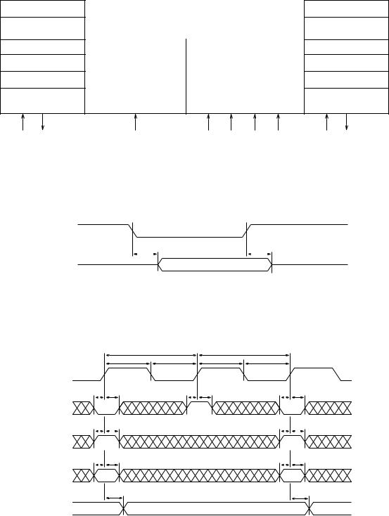
Figure 1. Synchronous Single-Port SRAM Output-Enable Timing
OEN
tlz |
|
thz |
Q[i]
Rising delays are measured at 50% of VDD and falling delays are measured at 50% of VDD.
Rising and falling slews are measured from 10% VDD to 90% VDD.
Figure 2. Synchronous Single-Port SRAM Read-Cycle Timing
CLK
CEN
WEN
A[j]
Q[i]
|
tcyc |
|
|
tcyc |
|
|
tckh |
tckl |
tckh |
tckl |
|
tcs |
tch |
tcs |
tch |
tcs |
tch |
tws |
twh |
|
|
tws |
twh |
tas |
tah |
|
|
tas |
tah |
ADD1 |
|
|
ADD2 |
||
|
ta |
|
|
|
ta |
|
Q1 |
|
|
|
Q2 |
Rising delays are measured at 50% of VDD and falling delays are measured at 50% of VDD. Rising and falling slews are measured from 10% VDD to 90% VDD.
Silterra Malaysia 0.18um Process SRAM-SP-HS Datasheet, Version 2003Q3V1
Copyright 1997-2003 Artisan Components, Inc.
2
RAM64x8
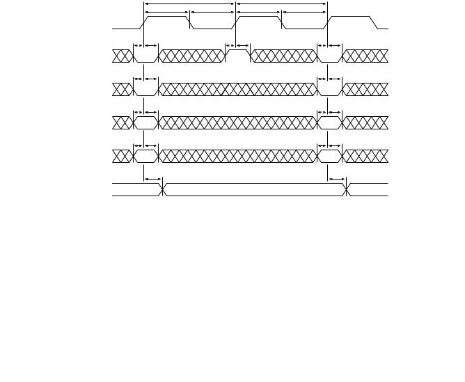
Synchronous Single-Port SRAM Write-Cycle Timing
CLK
CEN
WEN
A[j]
D[i]
Q[i]
|
tcyc |
|
|
tcyc |
|
|
tckh |
tckl |
tckh |
tckl |
|
tcs |
tch |
tcs |
tch |
tcs |
tch |
tws |
twh |
|
|
tws |
twh |
tas |
tah |
|
|
tas |
tah |
ADD1 |
|
|
ADD2 |
||
tds |
tdh |
|
|
tds |
tdh |
DATA1 |
|
|
DATA2 |
||
|
ta |
|
|
|
ta |
|
Q1 |
|
|
|
Q2 |
Rising signals are measured at 50% of VDD and falling signals are measured at 50% of VDD.
Rising and falling slews are measured from 10% VDD to 90% VDD.
SRAM Logic Table
CEN |
WEN |
OEN |
Data Out |
Mode |
Function |
|
|
|
|
|
|
|
|
|
|
|
|
|
Address inputs are disabled; data stored in the memory is |
|
H |
X |
L |
Last Data |
Standby |
retained, but the memory cannot be accessed for new reads or |
|
|
|
|
|
|
writes. Data outputs remain stable. |
|
|
|
|
|
|
|
|
|
|
|
|
|
Data on the data input bus D[n-1:0] is written to the memory |
|
L |
L |
L |
Data In |
Write |
location specified on the address bus A[m-1:0], and driven through |
|
|
|
|
|
|
to the data output bus Q[n-1:0]. |
|
|
|
|
|
|
|
|
L |
H |
L |
SRAM Data |
Read |
Data on the data output bus Q[n-1:0] is read from the memory |
|
location specified on the address bus A[m-1:0]. |
||||||
|
|
|
|
|
||
|
|
|
|
|
|
|
X |
X |
H |
Z |
High-Z |
The data output bus Q[n-1:0] is placed in a high impedance state. |
|
Other memory operations are unaffected. |
||||||
|
|
|
|
|
||
|
|
|
|
|
|
Silterra Malaysia 0.18um Process SRAM-SP-HS Datasheet, Version 2003Q3V1
Copyright 1997-2003 Artisan Components, Inc.
3

RAM64x8
SRAM Timing: Mission Mode
|
|
Fast Process |
|
Typical Process |
|
Slow Process |
|||
Parameter |
Symbol |
1.98V, 0˚C |
|
1.80V, 25˚C |
|
1.62V, 125˚C |
|||
|
|
Min (ns) |
Max (ns) |
|
Min (ns) |
Max (ns) |
|
Min (ns) |
Max (ns) |
|
|
|
|
|
|
|
|
|
|
Cycle time |
tcyc |
0.72 |
|
|
1.04 |
|
|
1.83 |
|
Access time1,2 |
ta |
0.67 |
|
|
|
1.09 |
|
|
1.88 |
Address setup |
tas |
0.19 |
|
|
0.32 |
|
|
0.60 |
|
Address hold |
tah |
0.06 |
|
|
0.08 |
|
|
0.12 |
|
Chip enable setup |
tcs |
0.25 |
|
|
0.35 |
|
|
0.59 |
|
Chip enable hold |
tch |
0.00 |
|
|
0.00 |
|
|
0.00 |
|
Write enable setup |
tws |
0.23 |
|
|
0.34 |
|
|
0.57 |
|
Write enable hold |
twh |
0.00 |
|
|
0.00 |
|
|
0.00 |
|
Data setup |
tds |
0.11 |
|
|
0.18 |
|
|
0.38 |
|
Data hold |
tdh |
0.00 |
|
|
0.00 |
|
|
0.00 |
|
Output enable to hi-Z |
thz |
|
0.42 |
|
|
0.61 |
|
|
0.99 |
Output enable active1 |
tlz |
|
0.37 |
|
|
0.53 |
|
|
0.87 |
Clock high |
tckh |
0.08 |
|
|
0.11 |
|
|
0.20 |
|
Clock low |
tckl |
0.11 |
|
|
0.18 |
|
|
0.31 |
|
Clock rise slew |
tckr |
|
4.00 |
|
|
4.00 |
|
|
4.00 |
Output load factor (ns/pF) |
Kload |
|
0.29 |
|
|
0.40 |
|
|
0.61 |
1 Parameters have a load dependence (Kload), which is used to calculate: TotalDelay = FixedDelay + (Kload × Cload ) .
2Access time is defined as the slowest possible output transition for the typical and slow corners, and the fastest possible output transition for the fast corner.
Silterra Malaysia 0.18um Process SRAM-SP-HS Datasheet, Version 2003Q3V1
Copyright 1997-2003 Artisan Components, Inc.
4

RAM64x8
Pin Capacitance
|
Fast Process |
|
Typical Process |
|
Slow Process |
Pin |
1.98V, 0˚C |
|
1.80V, 25˚C |
|
1.62V, 125˚C |
|
Value (pF) |
|
Value (pF) |
|
Value (pF) |
|
|
|
|
|
|
A[j] |
0.052 |
|
0.052 |
|
0.052 |
|
|
|
|
|
|
D[i] |
0.005 |
|
0.005 |
|
0.005 |
|
|
|
|
|
|
CLK |
0.178 |
|
0.164 |
|
0.144 |
|
|
|
|
|
|
CEN |
0.016 |
|
0.016 |
|
0.015 |
|
|
|
|
|
|
WEN |
0.015 |
|
0.015 |
|
0.015 |
|
|
|
|
|
|
OEN |
0.011 |
|
0.011 |
|
0.011 |
|
|
|
|
|
|
Q[i] |
0.024 |
|
0.024 |
|
0.023 |
|
|
|
|
|
|
Power
300.00MHz Operation
|
Fast Process |
|
Typical Process |
|
Slow Process |
Condition |
1.98V, 0˚C |
|
1.80V, 25˚C |
|
1.62V, 125˚C |
|
Value (mA) |
|
Value (mA) |
|
Value (mA) |
|
|
|
|
|
|
AC Current1 |
13.299 |
|
11.592 |
|
10.303 |
Read AC Current |
13.121 |
|
11.405 |
|
10.121 |
|
|
|
|
|
|
Write AC Current |
13.477 |
|
11.778 |
|
10.486 |
|
|
|
|
|
|
Peak Current |
120.899 |
|
73.719 |
|
39.640 |
|
|
|
|
|
|
Deselected Current2 |
4.956 |
|
4.209 |
|
3.701 |
Standby Current3 |
0.002 |
|
0.002 |
|
0.003 |
1Value assumes 50% read and write operations, where all addresses and 50% of input and output pins switch.
2Value assumes SRAM is deselected, all addresses switch, and 50% of input pins switch. The logic-switching component of deselected power becomes negligibly small if the input pins are held stable by externally controlling these signals with chip select.
3Value is independent of frequency and assumes all inputs and outputs are stable.
Clock Noise Limit
|
Fast Process |
|
Typical Process |
|
Slow Process |
|||
Signal |
1.98V, 0˚C |
|
1.80V, 25˚C |
|
1.62V, 125˚C |
|||
|
|
|
|
|
|
|
|
|
Pulse |
Voltage (V) |
|
Pulse |
Voltage (V) |
|
Pulse |
Voltage (V) |
|
|
|
|
||||||
|
Width (ns) |
|
Width (ns) |
|
Width (ns) |
|||
|
|
|
|
|
|
|
|
|
CLK |
10.000 |
0.853 |
|
10.000 |
0.861 |
|
10.000 |
0.822 |
|
|
|
|
|
|
|
|
|
The clock noise limit is the maximum CLK voltage allowable for the indicated pulse width without causing a spurious memory cycle or other memory failure.
Power and Ground Noise Limit
|
Fast Process |
|
Typical Process |
|
Slow Process |
Signal |
1.98V, 0˚C |
|
1.80V, 25˚C |
|
1.62V, 125˚C |
|
Voltage (V) |
|
Voltage (V) |
|
Voltage (V) |
|
|
|
|
|
|
Power |
0.198 |
|
0.180 |
|
0.162 |
|
|
|
|
|
|
Ground |
0.198 |
|
0.180 |
|
0.162 |
|
|
|
|
|
|
The power/ground noise limit is the maximum supply voltage transition allowable without causing a memory failure.
Silterra Malaysia 0.18um Process SRAM-SP-HS Datasheet, Version 2003Q3V1
Copyright 1997-2003 Artisan Components, Inc.
5