


ADS8326
www.ti.com |
SBAS343C –MAY 2007–REVISED SEPTEMBER 2009 |
DIGITAL INTERFACE
Signal Levels
The ADS8326 has a wide range of power-supply voltage. The A/D converter, as well as the digital interface circuit, is designed to accept and operate from 2.7V up to 5.5V. This voltage range will accommodate different logic levels. When the ADS8326 power-supply voltage is in the range of 4.5V to 5.5V (5V logic level), the ADS8326 can be connected directly to another 5V, CMOS-integrated circuit. When the ADS8326 power-supply voltage is in the range of 2.7V to 3.6V (3V logic level), the ADS8326 can be connected directly to another 3.3V LVCMOS integrated circuit.
Serial Interface
The ADS8326 communicates with microprocessors and other digital systems via a synchronous 3-wire serial interface, as illustrated in the Timing Information section. The DCLOCK signal synchronizes the data transfer, with each bit being transmitted on the falling edge of DCLOCK. Most receiving systems will capture the bitstream on the rising edge of DCLOCK. However, if the minimum hold time for DOUT is acceptable, the system can use the falling edge of DCLOCK to capture each bit.
A falling CS signal initiates the conversion and data transfer. The first 4.5 to 5.0 clock periods of the conversion cycle are used to sample the input signal. After the fifth falling DCLOCK edge, DOUT is enabled and will output a low value for one clock period. For the next 16 DCLOCK periods, DOUT will output the conversion result, most significant bit first. After the least significant bit (B0) has been output, subsequent clocks will repeat the output data, but in a least significant bit first format.
After the most significant bit (B15) has been repeated, DOUT will tri-state. Subsequent clocks will have no effect on the converter. A new conversion is initiated only when CS has been taken high and returned low.
Data Format
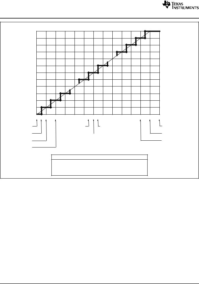
The output data from the ADS8326 is in Straight Binary format, as shown in Figure 43. This figure represents the ideal output code for a given input voltage and does not include the effects of offset, gain error, or noise.
Copyright © 2007–2009, Texas Instruments Incorporated |
Submit Documentation Feedback |
23 |
Product Folder Link(s): ADS8326
ADS8326 |
|
|
|
|
|
|
SBAS343C –MAY 2007 –REVISED SEPTEMBER 2009 |
|
|
|
www.ti.com |
||
|
Straight Binary |
|
|
|
|
|
|
1111 1111 1111 1111 |
|
|
|
65535 |
|
|
1111 1111 1111 1111 |
|
|
|
65534 |
|
|
1111 1111 1111 1111 |
|
|
|
65533 |
|
Code |
1000 0000 0000 0001 |
|
|
|
32769 |
|
|
|
|
|
|
|
|
DigitalOutput |
1000 0000 0000 0000 |
|
|
|
32768 |
Step |
0111 1111 1111 1111 |
|
|
|
32767 |
||
|
|
|
|
|
||
|
0000 0000 0000 0010 |
|
|
|
2 |
|
|
0000 0000 0000 0001 |
|
|
|
1 |
|
|
|
|
|
|
|
|
|
0000 0000 0000 0000 |
|
|
|
0 |
|
|
|
|
|
|
|
|
|
VZ = VCM = 0V |
2.499962V |
2.500038V |
VFS = VCM + VREF = 5V |
||
|
38.15µV |
|
VMS = VCM + VREF/2 = 2.5V |
VFS − 1LSB = 4.999924V |
||
|
|
|
|
|
||
|
76.29µV |
|
Unipolar Analog Input Voltage |
4.999847V |
||
|
|
|
|
|
||
|
152.58µV |
|
|
|
|
1LSB = 76.29µV |
|
|
|
|
|
|
VCM = 0V |
|
|
16-BIT |
|
|
|
VREF = 5V |
|
|
|
Straight Binary Output Unipolar Analog Input |
|
|
|
|
|
Zero Code |
VZ = 0000h |
VCODE = VCM |
|
|
|
|
Midscale Code |
VMS = 8000h |
VCODE = VCM + VREF/2 |
|
|
|
|
FullScale Code |
VFS = FFFFh |
VCODE = (VCM + VREF) − 1LSB |
|
|
Figure 43. Ideal Conversion Characteristics (Conditions: VCM = 0V, VREF = 5V)
24 |
Submit Documentation Feedback |
Copyright © 2007–2009, Texas Instruments Incorporated |
Product Folder Link(s): ADS8326