

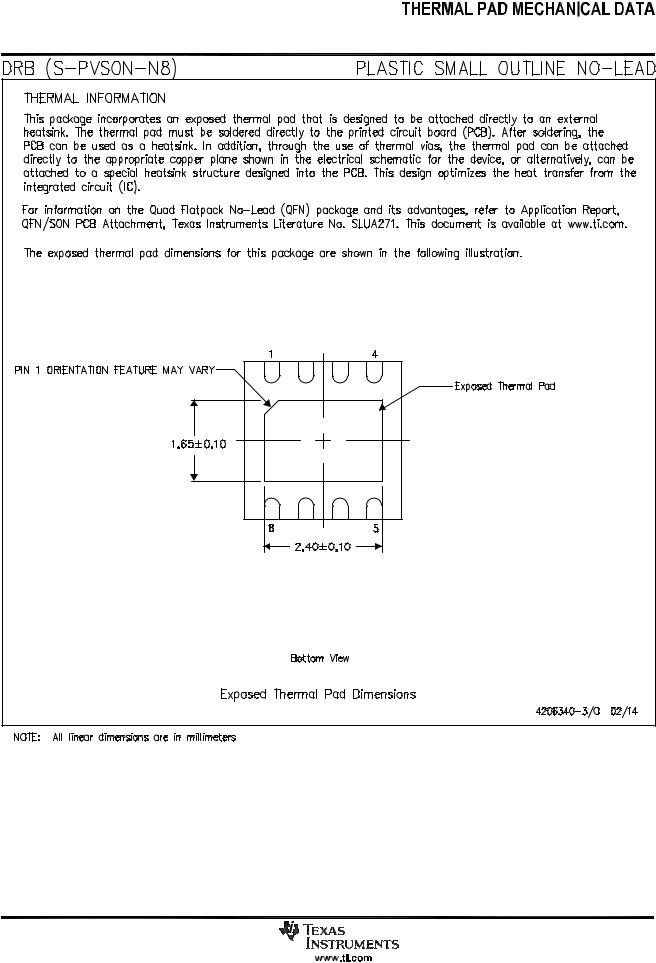
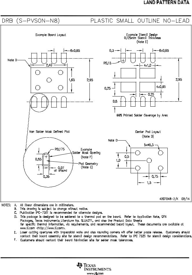
ADS8326
www.ti.com |
SBAS343C –MAY 2007–REVISED SEPTEMBER 2009 |
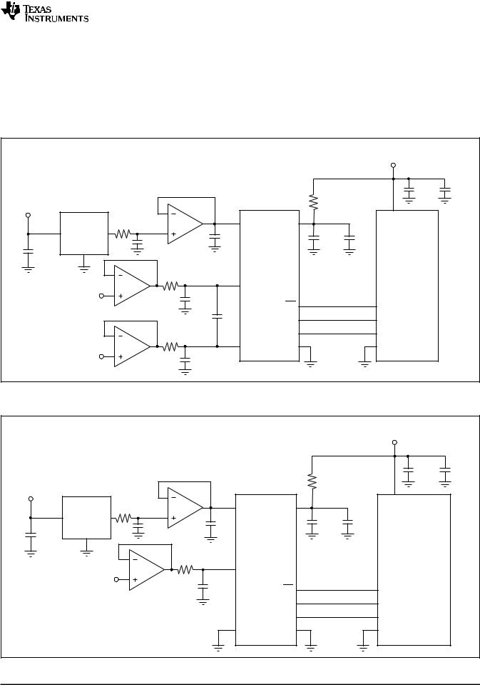
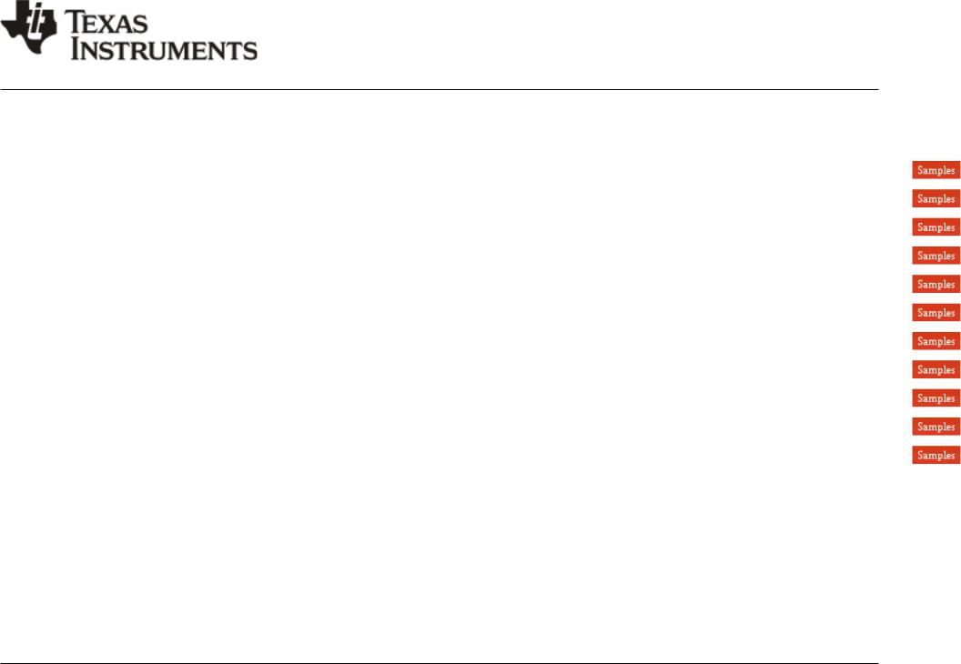
APPLICATION CIRCUITS
Figure 44 and Figure 45 show two examples of a basic data acquisition system. The ADS8326 input range is connected to 2.5V or 4.096V. The 5Ω resistor and 1μF to 10μF capacitor filters the microcontroller noise on the supply, as well as any
high-frequency noise from the supply itself. The exact values should be picked such that the filter provides adequate rejection of noise. Operational amplifiers and voltage reference are connected to analog power supply, AVDD.
|
|
|
|
|
|
|
DVDD |
|
|
|
|
|
|
|
|
2.7V to 3.6V |
|
|
|
|
|
|
|
|
0.1µF |
+ |
|
|
|
|
|
|
|
10µF |
|
AVDD |
|
|
|
|
|
5Ω |
|
|
2.7V to 5V |
|
|
|
|
|
|
|
|
|
REF3225 |
|
|
REF |
|
|
|
|
|
|
10Ω |
OPA350 |
VDD |
|
|
||
|
|
|
|
|
+ |
|
||
IN |
OUT |
|
47µF |
|
|
0.1µF |
|
|
|
|
|
|
|
10µF |
|
||
|
|
|
2.2µF |
|
|
|
|
|
0.47µF |
GND |
|
|
|
ADS8326 |
|
|
|
|
|
|
|
|
|
|||
|
|
|
|
|
|
|
DSP |
|
|
|
|
10Ω |
|
|
|
TMS320C6XX |
|
|
|
OPA365 |
|
+IN |
|
|
or |
|
VCM + (0V to 2.5V) |
|
1000pF |
|
|
|
TMS320C5XX |
|
|
|
|
|
|
|
|
|||
|
|
|
|
|
CS |
or |
|
|
|
|
|
|
|
|
|
||
|
|
|
|
|
|
|
|
|
|
|
|
1nF |
|
|
|
TMS320C2XX |
|
|
|
|
|
|
DOUT |
|
|
|
|
|
|
|
|
|
|
|
|
|
|
|
10Ω |
|
|
DCLOCK |
|
|
|
|
|
|
|
|
|
|
|
|
|
OPA365 |
|
−IN |
|
GND |
GND |
|
|
VCM |
|
1000pF |
|
|
|
|
|
|
|
|
|
|
|
|
|
|
Figure 44. Basic Data Acquisition System: Example 1
|
|
|
|
|
|
DVDD |
|
|
|
|
|
|
|
4.5V to 5.5V |
|
|
|
|
|
|
|
0.1µF |
+ |
|
|
|
|
|
|
10µF |
|
AVDD |
|
|
|
|
5Ω |
|
|
4.3V to 5.5V |
|
|
|
|
|
|
|
|
REF3240 |
|
REF |
|
|
|
|
|
10Ω |
OPA350 |
VDD |
|
|
||
|
|
|
|
+ |
|
||
IN |
OUT |
|
|
|
0.1µF |
|
|
|
|
2.2µF |
47µF |
|
10µF |
|
|
|
|
|
|
|
|
||
0.47µF |
GND |
|
|
ADS8326 |
|
|
|
|
|
|
|
|
|||
|
|
10Ω |
|
|
|
Microcontroller |
|
|
|
|
+IN |
|
|
|
|
|
|
OPA365 |
|
|
or |
|
|
|
|
|
|
|
|
|
|
|
0V to 4.096V |
|
|
|
|
DSP |
|
|
|
|
1000pF |
|
CS |
|
|
|
|
|
|
|
|
|
|
|
|
|
|
|
DOUT |
|
|
|
|
|
|
|
DCLOCK |
|
|
|
|
|
−IN |
|
GND |
GND |
|
Figure 45. Basic Data Acquisition System: Example 2
Copyright © 2007–2009, Texas Instruments Incorporated |
Submit Documentation Feedback |
27 |
Product Folder Link(s): ADS8326

ADS8326 |
|
SBAS343C –MAY 2007 –REVISED SEPTEMBER 2009 |
www.ti.com |
REVISION HISTORY |
|
NOTE: Page numbers for previous revisions may differ from page numbers in the current version. |
|
Changes from Revision B (May, 2008) to Revision C |
Page |
• Released SON-8 package; changed statements regarding SON-8 package availability ..................................................... |
1 |
• Deleted footnote about SON-8 package availability ............................................................................................................. |
2 |
• Deleted footnote about SON-8 package availability ............................................................................................................. |
3 |
• Deleted footnote about SON-8 package availability ............................................................................................................. |
7 |
Changes from Revision A (August, 2007) to Revision B |
Page |
• Changed SON-8 package availability to Q3, 2008 ............................................................................................................... |
1 |
• Changed y-axis unit in Figure 35 from μA to mA ............................................................................................................... |
18 |
• Added Power-On Reset section ......................................................................................................................................... |
25 |
28 |
Submit Documentation Feedback |
Copyright © 2007–2009, Texas Instruments Incorporated |
Product Folder Link(s): ADS8326
PACKAGE OPTION ADDENDUM
www.ti.com |
10-Jun-2014 |
PACKAGING INFORMATION
Orderable Device |
Status |
Package Type |
Package |
Pins |
Package |
Eco Plan |
Lead/Ball Finish |
MSL Peak Temp |
Op Temp (°C) |
Device Marking |
Samples |
|
(1) |
|
Drawing |
|
Qty |
(2) |
(6) |
(3) |
|
(4/5) |
|
ADS8326IBDGKR |
ACTIVE |
VSSOP |
DGK |
8 |
2500 |
Green (RoHS |
CU NIPDAU | |
Level-2-260C-1 YEAR |
-40 to 85 |
D26 |
|
|
|
|
|
|
|
& no Sb/Br) |
CU NIPDAUAG |
|
|
|
|
ADS8326IBDGKT |
ACTIVE |
VSSOP |
DGK |
8 |
250 |
Green (RoHS |
CU NIPDAU | |
Level-2-260C-1 YEAR |
-40 to 85 |
D26 |
|
|
|
|
|
|
|
& no Sb/Br) |
CU NIPDAUAG |
|
|
|
|
ADS8326IBDGKTG4 |
ACTIVE |
VSSOP |
DGK |
8 |
250 |
Green (RoHS |
CU NIPDAU |
Level-2-260C-1 YEAR |
-40 to 85 |
D26 |
|
|
|
|
|
|
|
& no Sb/Br) |
|
|
|
|
|
ADS8326IBDRBR |
ACTIVE |
SON |
DRB |
8 |
3000 |
Green (RoHS |
CU NIPDAU |
Level-2-260C-1 YEAR |
-40 to 85 |
D26 |
|
|
|
|
|
|
|
& no Sb/Br) |
|
|
|
|
|
ADS8326IBDRBT |
ACTIVE |
SON |
DRB |
8 |
250 |
Green (RoHS |
CU NIPDAU |
Level-2-260C-1 YEAR |
-40 to 85 |
D26 |
|
|
|
|
|
|
|
& no Sb/Br) |
|
|
|
|
|
ADS8326IDGKR |
ACTIVE |
VSSOP |
DGK |
8 |
2500 |
Green (RoHS |
CU NIPDAU | |
Level-2-260C-1 YEAR |
-40 to 85 |
D26 |
|
|
|
|
|
|
|
& no Sb/Br) |
CU NIPDAUAG |
|
|
|
|
ADS8326IDGKRG4 |
ACTIVE |
VSSOP |
DGK |
8 |
2500 |
Green (RoHS |
CU NIPDAU |
Level-2-260C-1 YEAR |
-40 to 85 |
D26 |
|
|
|
|
|
|
|
& no Sb/Br) |
|
|
|
|
|
ADS8326IDGKT |
ACTIVE |
VSSOP |
DGK |
8 |
250 |
Green (RoHS |
CU NIPDAU | |
Level-2-260C-1 YEAR |
-40 to 85 |
D26 |
|
|
|
|
|
|
|
& no Sb/Br) |
CU NIPDAUAG |
|
|
|
|
ADS8326IDGKTG4 |
ACTIVE |
VSSOP |
DGK |
8 |
250 |
Green (RoHS |
CU NIPDAU |
Level-2-260C-1 YEAR |
-40 to 85 |
D26 |
|
|
|
|
|
|
|
& no Sb/Br) |
|
|
|
|
|
ADS8326IDRBR |
ACTIVE |
SON |
DRB |
8 |
3000 |
Green (RoHS |
CU NIPDAU |
Level-2-260C-1 YEAR |
-40 to 85 |
D26 |
|
|
|
|
|
|
|
& no Sb/Br) |
|
|
|
|
|
ADS8326IDRBT |
ACTIVE |
SON |
DRB |
8 |
250 |
Green (RoHS |
CU NIPDAU |
Level-2-260C-1 YEAR |
-40 to 85 |
D26 |
|
|
|
|
|
|
|
& no Sb/Br) |
|
|
|
|
|
(1)The marketing status values are defined as follows:
ACTIVE: Product device recommended for new designs.
LIFEBUY: TI has announced that the device will be discontinued, and a lifetime-buy period is in effect.
NRND: Not recommended for new designs. Device is in production to support existing customers, but TI does not recommend using this part in a new design.
PREVIEW: Device has been announced but is not in production. Samples may or may not be available.
OBSOLETE: TI has discontinued the production of the device.
(2)Eco Plan - The planned eco-friendly classification: Pb-Free (RoHS), Pb-Free (RoHS Exempt), or Green (RoHS & no Sb/Br) - please check http://www.ti.com/productcontent for the latest availability information and additional product content details.
TBD: The Pb-Free/Green conversion plan has not been defined.
Pb-Free (RoHS): TI's terms "Lead-Free" or "Pb-Free" mean semiconductor products that are compatible with the current RoHS requirements for all 6 substances,including the requirement that lead not exceed 0.1% by weight in homogeneous materials. Where designed to be soldered at high temperatures, TI Pb-Free products are suitable for use in specified lead-free processes.
Addendum-Page 1
PACKAGE OPTION ADDENDUM
www.ti.com |
10-Jun-2014 |
Pb-Free (RoHS Exempt): This component has a RoHS exemption for either 1) lead-based flip-chip solder bumps used between the die and package, or 2) lead-based die adhesive used between the die and leadframe. The component is otherwise considered Pb-Free (RoHS compatible) as defined above.
Green (RoHS & no Sb/Br): TI defines "Green" to mean Pb-Free (RoHS compatible), and free of Bromine (Br) and Antimony (Sb) based flame retardants (Br or Sb do not exceed 0.1% by weight in homogeneous material)
(3)MSL, Peak Temp. - The Moisture Sensitivity Level rating according to the JEDEC industry standard classifications, and peak solder temperature.
(4)There may be additional marking, which relates to the logo, the lot trace code information, or the environmental category on the device.
(5)Multiple Device Markings will be inside parentheses. Only one Device Marking contained in parentheses and separated by a "~" will appear on a device. If a line is indented then it is a continuation of the previous line and the two combined represent the entire Device Marking for that device.
(6)Lead/Ball Finish - Orderable Devices may have multiple material finish options. Finish options are separated by a vertical ruled line. Lead/Ball Finish values may wrap to two lines if the finish value exceeds the maximum column width.
Important Information and Disclaimer:The information provided on this page represents TI's knowledge and belief as of the date that it is provided. TI bases its knowledge and belief on information provided by third parties, and makes no representation or warranty as to the accuracy of such information. Efforts are underway to better integrate information from third parties. TI has taken and continues to take reasonable steps to provide representative and accurate information but may not have conducted destructive testing or chemical analysis on incoming materials and chemicals. TI and TI suppliers consider certain information to be proprietary, and thus CAS numbers and other limited information may not be available for release.
In no event shall TI's liability arising out of such information exceedthe total purchase price of the TI part(s) at issue in this document sold by TI to Customer on an annual basis.
Addendum-Page 2
PACKAGE MATERIALS INFORMATION
www.ti.com |
6-Nov-2013 |
|
|
TAPE AND REEL INFORMATION
*All dimensions are nominal
Device |
Package |
Package |
Pins |
SPQ |
Reel |
Reel |
A0 |
B0 |
K0 |
P1 |
W |
Pin1 |
|
Type |
Drawing |
|
|
Diameter |
Width |
(mm) |
(mm) |
(mm) |
(mm) |
(mm) |
Quadrant |
|
|
|
|
|
(mm) |
W1 (mm) |
|
|
|
|
|
|
ADS8326IBDGKR |
VSSOP |
DGK |
8 |
2500 |
330.0 |
12.4 |
5.3 |
3.4 |
1.4 |
8.0 |
12.0 |
Q1 |
|
|
|
|
|
|
|
|
|
|
|
|
|
ADS8326IBDGKT |
VSSOP |
DGK |
8 |
250 |
180.0 |
12.4 |
5.3 |
3.4 |
1.4 |
8.0 |
12.0 |
Q1 |
|
|
|
|
|
|
|
|
|
|
|
|
|
ADS8326IBDRBR |
SON |
DRB |
8 |
3000 |
330.0 |
12.4 |
3.3 |
3.3 |
1.1 |
8.0 |
12.0 |
Q2 |
ADS8326IBDRBT |
SON |
DRB |
8 |
250 |
180.0 |
12.4 |
3.3 |
3.3 |
1.1 |
8.0 |
12.0 |
Q2 |
ADS8326IDGKR |
VSSOP |
DGK |
8 |
2500 |
330.0 |
12.4 |
5.3 |
3.4 |
1.4 |
8.0 |
12.0 |
Q1 |
|
|
|
|
|
|
|
|
|
|
|
|
|
ADS8326IDGKT |
VSSOP |
DGK |
8 |
250 |
180.0 |
12.4 |
5.3 |
3.4 |
1.4 |
8.0 |
12.0 |
Q1 |
|
|
|
|
|
|
|
|
|
|
|
|
|
ADS8326IDRBR |
SON |
DRB |
8 |
3000 |
330.0 |
12.4 |
3.3 |
3.3 |
1.1 |
8.0 |
12.0 |
Q2 |
ADS8326IDRBT |
SON |
DRB |
8 |
250 |
180.0 |
12.4 |
3.3 |
3.3 |
1.1 |
8.0 |
12.0 |
Q2 |
|
|
|
|
|
|
|
|
|
|
|
|
|
Pack Materials-Page 1
PACKAGE MATERIALS INFORMATION
www.ti.com |
6-Nov-2013 |
|
|
*All dimensions are nominal
Device |
Package Type |
Package Drawing |
Pins |
SPQ |
Length (mm) |
Width (mm) |
Height (mm) |
|
|
|
|
|
|
|
|
ADS8326IBDGKR |
VSSOP |
DGK |
8 |
2500 |
367.0 |
367.0 |
35.0 |
ADS8326IBDGKT |
VSSOP |
DGK |
8 |
250 |
210.0 |
185.0 |
35.0 |
|
|
|
|
|
|
|
|
ADS8326IBDRBR |
SON |
DRB |
8 |
3000 |
338.1 |
338.1 |
20.6 |
|
|
|
|
|
|
|
|
ADS8326IBDRBT |
SON |
DRB |
8 |
250 |
210.0 |
185.0 |
35.0 |
ADS8326IDGKR |
VSSOP |
DGK |
8 |
2500 |
367.0 |
367.0 |
35.0 |
|
|
|
|
|
|
|
|
ADS8326IDGKT |
VSSOP |
DGK |
8 |
250 |
210.0 |
185.0 |
35.0 |
|
|
|
|
|
|
|
|
ADS8326IDRBR |
SON |
DRB |
8 |
3000 |
338.1 |
338.1 |
20.6 |
ADS8326IDRBT |
SON |
DRB |
8 |
250 |
210.0 |
185.0 |
35.0 |
|
|
|
|
|
|
|
|
Pack Materials-Page 2


IMPORTANT NOTICE
Texas Instruments Incorporated and its subsidiaries (TI) reserve the right to make corrections, enhancements, improvements and other changes to its semiconductor products and services per JESD46, latest issue, and to discontinue any product or service per JESD48, latest issue. Buyers should obtain the latest relevant information before placing orders and should verify that such information is current and complete. All semiconductor products (also referred to herein as “components”) are sold subject to TI’s terms and conditions of sale supplied at the time of order acknowledgment.
TI warrants performance of its components to the specifications applicable at the time of sale, in accordance with the warranty in TI’s terms and conditions of sale of semiconductor products. Testing and other quality control techniques are used to the extent TI deems necessary to support this warranty. Except where mandated by applicable law, testing of all parameters of each component is not necessarily performed.
TI assumes no liability for applications assistance or the design of Buyers’ products. Buyers are responsible for their products and applications using TI components. To minimize the risks associated with Buyers’ products and applications, Buyers should provide adequate design and operating safeguards.
TI does not warrant or represent that any license, either express or implied, is granted under any patent right, copyright, mask work right, or other intellectual property right relating to any combination, machine, or process in which TI components or services are used. Information published by TI regarding third-party products or services does not constitute a license to use such products or services or a warranty or endorsement thereof. Use of such information may require a license from a third party under the patents or other intellectual property of the third party, or a license from TI under the patents or other intellectual property of TI.
Reproduction of significant portions of TI information in TI data books or data sheets is permissible only if reproduction is without alteration and is accompanied by all associated warranties, conditions, limitations, and notices. TI is not responsible or liable for such altered documentation. Information of third parties may be subject to additional restrictions.
Resale of TI components or services with statements different from or beyond the parameters stated by TI for that component or service voids all express and any implied warranties for the associated TI component or service and is an unfair and deceptive business practice. TI is not responsible or liable for any such statements.
Buyer acknowledges and agrees that it is solely responsible for compliance with all legal, regulatory and safety-related requirements concerning its products, and any use of TI components in its applications, notwithstanding any applications-related information or support that may be provided by TI. Buyer represents and agrees that it has all the necessary expertise to create and implement safeguards which anticipate dangerous consequences of failures, monitor failures and their consequences, lessen the likelihood of failures that might cause harm and take appropriate remedial actions. Buyer will fully indemnify TI and its representatives against any damages arising out of the use of any TI components in safety-critical applications.
In some cases, TI components may be promoted specifically to facilitate safety-related applications. With such components, TI’s goal is to help enable customers to design and create their own end-product solutions that meet applicable functional safety standards and requirements. Nonetheless, such components are subject to these terms.
No TI components are authorized for use in FDA Class III (or similar life-critical medical equipment) unless authorized officers of the parties have executed a special agreement specifically governing such use.
Only those TI components which TI has specifically designated as military grade or “enhanced plastic” are designed and intended for use in military/aerospace applications or environments. Buyer acknowledges and agrees that any military or aerospace use of TI components which have not been so designated is solely at the Buyer's risk, and that Buyer is solely responsible for compliance with all legal and regulatory requirements in connection with such use.
TI has specifically designated certain components as meeting ISO/TS16949 requirements, mainly for automotive use. In any case of use of non-designated products, TI will not be responsible for any failure to meet ISO/TS16949.
Products |
|
Applications |
|
Audio |
www.ti.com/audio |
Automotive and Transportation |
www.ti.com/automotive |
Amplifiers |
amplifier.ti.com |
Communications and Telecom |
www.ti.com/communications |
Data Converters |
dataconverter.ti.com |
Computers and Peripherals |
www.ti.com/computers |
DLP® Products |
www.dlp.com |
Consumer Electronics |
www.ti.com/consumer-apps |
DSP |
dsp.ti.com |
Energy and Lighting |
www.ti.com/energy |
Clocks and Timers |
www.ti.com/clocks |
Industrial |
www.ti.com/industrial |
Interface |
interface.ti.com |
Medical |
www.ti.com/medical |
Logic |
logic.ti.com |
Security |
www.ti.com/security |
Power Mgmt |
power.ti.com |
Space, Avionics and Defense |
www.ti.com/space-avionics-defense |
Microcontrollers |
microcontroller.ti.com |
Video and Imaging |
www.ti.com/video |
RFID |
www.ti-rfid.com |
|
|
OMAP Applications Processors |
www.ti.com/omap |
TI E2E Community |
e2e.ti.com |
Wireless Connectivity |
www.ti.com/wirelessconnectivity |
|
|
Mailing Address: Texas Instruments, Post Office Box 655303, Dallas, Texas 75265
Copyright © 2014, Texas Instruments Incorporated