

бакМИТ_КП2015 / Компоненты по вариантам / АЦП / AD7893-5
.pdfa |
LC2MOS 12-Bit, Serial 6 ms |
|
ADC in 8-Pin Package |
||
|
|
|
|
|
AD7893 |
|
|
|
FEATURES
Fast 12-Bit ADC with 6 ms Conversion Time
8-Pin Mini-DlP and SOIC
Single Supply Operation
High Speed, Easy-to-Use, Serial Interface On-Chip Track/Hold Amplifier
Selection of Input Ranges 610 V for AD7893-10 62.5 V for AD7893-3
0 V to +2.5 V for AD7893-2
0 V to +5 V for AD7893-5 Low Power: 25 mW typ
FUNCTIONAL BLOCK DIAGRAM
|
|
REF IN |
|
VDD |
|
AD7893 |
|
|
|
|
|
TRACK/ |
|
|
VIN |
SIGNAL |
HOLD |
|
|
|
|
|
||
|
SCALING* |
|
12-BIT |
|
|
|
|
ADC |
|
CONVST |
|
|
OUTPUT |
|
|
|
REGISTER |
||
|
|
|
||
|
AGND DGND |
|
SCLK |
SDATA |
*AD7893-5, AD7893-10, AD7893-3 |
|
|
||
GENERAL DESCRIPTION
The AD7893 is a fast, 12-bit ADC that operates from a single +5 V supply and is housed in a small 8-pin mini-DIP and 8-pin SOIC. The part contains a 6 μs successive approximation A/D converter, an on-chip track/hold amplifier, an on-chip clock and a high speed serial interface.
Output data from the AD7893 is provided via a high speed, serial interface port. This two-wire serial interface has a serial clock input and a serial data output with the external serial clock accessing the serial data from the part.
In addition to traditional dc accuracy specifications such as linearity, full-scale and offset errors, the AD7893 is also specified for dynamic performance parameters, including harmonic distortion and signal-to-noise ratio.
The part accepts an analog input range of ±10 V (AD7893-10),
±2.5 V (AD7893-3), 0 V to +5 V (AD7893-5) or 0 V to +2.5 V (AD7893-2) and operates from a single +5 V supply, consuming only 25 mW typical.
The AD7893 is fabricated in Analog Devices’ Linear Compatible CMOS (LC2MOS) process, a mixed technology process that combines precision bipolar circuits with low power CMOS logic. The part is available in a small, 8-pin, 0.3" wide, plastic or hermetic dual-in-line package (mini-DIP) and in an 8-pin, small outline IC (SOIC).
REV. E
Information furnished by Analog Devices is believed to be accurate and reliable. However, no responsibility is assumed by Analog Devices for its use, nor for any infringements of patents or other rights of third parties which may result from its use. No license is granted by implication or otherwise under any patent or patent rights of Analog Devices.
PRODUCT HIGHLIGHTS
1.Fast, 12-Bit ADC in 8-Pin Package
The AD7893 contains a 6 μs ADC, a track/hold amplifier, control logic and a high speed serial interface, all in an 8-pin package. This offers considerable space saving over alternative solutions.
2.Low Power, Single Supply Operation
The AD7893 operates from a single +5 V supply and consumes only 25 mW. This low power, single supply operation makes it ideal for battery powered or portable applications.
3.High Speed Serial Interface
The part provides high speed serial data and serial clock lines, allowing for an easy, two-wire serial interface arrangement.
One Technology Way, P.O. Box 9106, Norwood, MA 02062-9106, U.S.A.
Tel: 617/329-4700 |
World Wide Web Site: http://www.analog.com |
Fax: 617/326-8703 |
© Analog Devices, Inc., 1997 |
AD7893–SPECIFICATIONS (VDD = +5 V, AGND = DGND = 0 V, REF IN = +2.5 V. All specifications TMIN to TMAX unless otherwise noted.)
|
A |
B |
S |
|
|
Parameter |
Versionsl |
Versions |
Version |
Units |
Test Conditions/Comments |
|
|
|
|
|
|
DYNAMIC PERFORMANCE |
|
|
|
|
|
Signal to (Noise + Distortion) Ratio2 |
|
|
|
|
|
@ +25°C |
70 |
70 |
70 |
dB min |
fIN = 10 kHz Sine Wave, fSAMPLE = 117 kHz |
Total Harmonic Distortion (THD)2 |
–80 |
–80 |
–80 |
dB max |
fIN = 10 kHz Sine Wave, fSAMPLE = 117 kHz |
Peak Harmonic or Spurious Noise2 |
–80 |
–80 |
–80 |
dB max |
fIN = 10 kHz Sine Wave, fSAMPLE = 117 kHz |
Intermodulation Distortion (IMD)2 |
|
|
|
|
fa = 9 kHz, fb = 9.5 kHz, fSAMPLE = 117 kHz |
2nd Order Terms |
–80 |
–80 |
–80 |
dB max |
|
3rd Order Terms |
–80 |
–80 |
–80 |
dB max |
|
|
|
|
|
|
|
DC ACCURACY |
|
|
|
|
|
Resolution |
12 |
12 |
12 |
Bits |
|
Minimum Resolution for which |
|
|
|
|
|
No Missing Codes are Guaranteed |
12 |
12 |
12 |
Bits |
|
Relative Accuracy2 |
±1 |
±1/2 |
±1 |
LSB max |
|
Differential Nonlinearity2 |
±1 |
±1 |
±1 |
LSB max |
|
Positive Full-Scale Error2 |
±3 |
±1.5 |
±3 |
LSB max |
|
AD7893-2, AD7893-5 |
±4 |
±3 |
±4 |
|
|
Unipolar Offset Error |
LSB max |
|
|||
AD7893-10, AD7893-3 |
±3 |
±1.5 |
±3 |
|
|
Negative Full-Scale Error2 |
LSB max |
|
|||
Bipolar Zero Error |
±4 |
±2 |
±4 |
LSB max |
|
ANALOG INPUT |
|
|
|
|
|
AD7893-10 |
±10 |
±10 |
±10 |
|
|
Input Voltage Range |
Volts |
|
|||
Input Resistance |
16 |
16 |
16 |
kΩ min |
|
AD7893-3 |
±2.5 |
±2.5 |
±2.5 |
|
|
Input Voltage Range |
Volts |
|
|||
Input Resistance |
4 |
4 |
4 |
kΩ min |
|
AD7893-5 |
|
|
|
|
|
Input Voltage Range |
0 to +5 |
0 to +5 |
0 to +5 |
Volts |
|
Input Resistance |
9 |
9 |
9 |
kΩ min |
|
AD7893-2 |
|
|
|
|
|
Input Voltage Range |
0 to +2.5 |
0 to +2.5 |
0 to +2.5 |
Volts |
|
Input Current |
500 |
500 |
500 |
nA max |
|
|
|
|
|
|
|
REFERENCE INPUT |
|
|
|
|
2.5 V ± 5% |
REF IN Input Voltage Range |
2.375/2.625 |
2.375/2.625 |
2.375/2.625 |
V min/V max |
|
Input Current |
2 |
2 |
10 |
μA max |
|
Input Capacitance3 |
10 |
10 |
10 |
pF max |
|
LOGIC INPUTS |
|
|
|
|
VDD = 5 V ± 5% |
Input High Voltage, VINH |
2.4 |
2.4 |
2.4 |
V min |
|
Input Low Voltage, VINL |
0.8 |
0.8 |
0.8 |
V max |
VDD = 5 V ± 5% |
Input Current, IIN |
±10 |
±10 |
±10 |
μA max |
VIN = 0 V to VDD |
Input Capacitance, CIN3 |
10 |
10 |
10 |
pF max |
|
LOGIC OUTPUTS |
|
|
|
|
ISOURCE = 200 μA |
Output High Voltage, VOH |
4.0 |
4.0 |
4.0 |
V min |
|
Output Low Voltage, VOL |
0.4 |
0.4 |
0.4 |
V max |
ISINK = 1.6 mA |
Output Coding |
|
|
|
|
|
AD7893-10, AD7893-3 |
2s Complement |
|
|
|
|
AD7893-2, AD7893-5 |
Straight (Natural) Binary |
|
|
|
|
|
|
|
|
|
|
CONVERSION RATE |
|
|
|
μs max |
|
Conversion Time |
6 |
6 |
6 |
|
|
Track/Hold Acquisition Time2 |
1.5 |
1.5 |
1.5 |
μs max |
|
POWER REQUIREMENTS |
|
|
|
|
±5% for Specified Performance |
VDD |
+5 |
+5 |
+5 |
V nom |
|
IDD |
9 |
9 |
9 |
mA max |
|
Power Dissipation |
45 |
45 |
45 |
mW max |
Typically 25 mW |
|
|
|
|
|
|
NOTES
1Temperature Ranges are as follows: A, B Versions: –40°C to +85°C, S Version: –55°C to +125°C. 2See Terminology.
3Sample tested @ +25°C to ensure compliance. Specifications subject to change without notice.
–2–
REV. E
AD7893
TIMING CHARACTERISTICS1, 2 (VDD = +5 V, AGND = DGND = 0 V, REF IN = +2.5 V)
|
A, B |
S |
|
|
|
|
Parameter |
Versions |
Version |
Units |
Test Conditions/Comments |
||
|
|
|
|
|
|
|
t1 |
50 |
50 |
ns min |
|
|
Pulse Width |
|
CONVST |
|||||
t2 |
60 |
70 |
ns min |
|
SCLK High Pulse Width |
|
t3 |
30 |
40 |
ns min |
|
SCLK Low Pulse Width |
|
t43 |
50 |
60 |
ns max |
|
SCLK Rising Edge to Data Valid Delay |
|
t54 |
10 |
10 |
ns min |
|
Bus Relinquish Time after Falling Edge of SCLK |
|
|
100 |
100 |
ns max |
|
|
|
|
|
|
|
|
|
|
NOTES
1Sample tested at +25°C to ensure compliance. All input signals are measured with tr = tf = 1 ns (10% to 90% of +5 V) and timed from a voltage level of +1.6 V.
2See Figure 5.
3Measured with the load circuit of Figure 1 and defined as the time required for an output to cross 0.8 V or 2.4 V.
4Derived from the measured time taken by the data outputs to change 0.5 V when loaded with the circuit of Figure 1. The measured number is then extrapolated back
to remove the effects of charging or discharging the 50 pF capacitor. This means that the time, t 5, quoted in the timing characteristics is the true bus relinquish time of the part and, as such, is independent of external bus loading capacitances.
ABSOLUTE MAXIMUM RATINGS*
(TA = +25°C unless otherwise noted) |
|
VDD to AGND . . . . . . . . . . . . . . . . . . . . |
. . . . . –0.3 V to +7 V |
VDD to DGND . . . . . . . . . . . . . . . . . . . . . |
. . . . –0.3 V to +7 V |
Analog Input Voltage to AGND |
±17 V |
AD7893-10, AD7893-5 . . . . . . . . . . . . |
|
AD7893-2, AD7893-3 . . . . . . . . . . . . . |
. . . . . . –5 V, +10 V |
Reference Input Voltage to AGND . . . |
–0.3 V to VDD + 0.3 V |
Digital Input Voltage to DGND . . . . . |
–0.3 V to VDD + 0.3 V |
Digital Output Voltage to DGND . . . . |
–0.3 V to VDD + 0.3 V |
Operating Temperature Range |
–40°C to +85°C |
Commercial (A, B Versions) . . . . . . . . |
|
Extended (S Version) . . . . . . . . . . . . . . |
. . –55°C to +125°C |
Storage Temperature Range . . . . . . . . . . |
. . –65°C to +150°C |
Junction Temperature . . . . . . . . . . . . . . . |
. . . . . . . . . . +150°C |
Plastic DIP Package, Power Dissipation . |
. . . . . . . . . 450 mW |
θJA Thermal Impedance . . . . . . . . . . . . |
. . . . . . . . . 130°C/W |
Lead Temperature (Soldering, 10 sec) . |
. . . . . . . . . . +260°C |
Cerdip Package, Power Dissipation . . . . . |
. . . . . . . . . 450 mW |
θJA Thermal Impedance . . . . . . . . . . . . |
. . . . . . . . . 125°C/W |
Lead Temperature (Soldering, 10 sec) . |
. . . . . . . . . . +300°C |
SOIC Package, Power Dissipation . . . . . . |
. . . . . . . . . 450 mW |
θJA Thermal Impedance . . . . . . . . . . . . |
. . . . . . . . . 170°C/W |
Lead Temperature, Soldering |
+215°C |
Vapor Phase (60 sec) . . . . . . . . . . . . |
|
Infrared (15 sec) . . . . . . . . . . . . . . . . |
. . . . . . . . . . +220°C |
*Stresses above those listed under “Absolute Maximum Ratings” may cause permanent damage to the device. This is a stress rating only; functional operation of the device at these or any other conditions above those listed in the operational sections of this specification is not implied. Exposure to absolute maximum rating conditions for extended periods may affect device reliability.
 1.6mA
1.6mA
TO
OUTPUT 


 +2.1V PIN
50pF
 200µA
200µA
Figure 1. Load Circuit for Access Time and Bus Relinquish Time
CAUTION
ESD (electrostatic discharge) sensitive device. Electrostatic charges as high as 4000 V readily accumulate on the human body and test equipment and can discharge without detection. Although the AD7893 features proprietary ESD protection circuitry, permanent damage may occur on devices subjected to high energy electrostatic discharges. Therefore, proper ESD precautions are recommended to avoid performance degradation or loss of functionality.
WARNING!
ESD SENSITIVE DEVICE
REV. E |
–3– |

AD7893
|
|
|
|
|
PIN FUNCTION DESCRIPTION |
|
|
|
|||||||||
Pin |
|
Pin |
|
|
|
|
|
|
|
|
|
|
|
|
|
|
|
No. |
|
Mnemonic |
Description |
|
|
|
|
|
|
|
|
|
|
|
|
||
|
|
|
|
|
|
|
|
|
|
|
|
|
|
|
|
|
|
1 |
|
REF IN |
Voltage Reference Input. An external reference source should be connected to this pin to provide the refer- |
||||||||||||||
|
|
|
|
ence voltage for the AD7893’s conversion process. The REF IN input is buffered on-chip. The nominal ref- |
|||||||||||||
|
|
|
|
erence voltage for correct operation of the AD7893 is +2.5 V. |
|
|
|||||||||||
2 |
|
VIN |
Analog Input Channel. The analog input range is ±10 V (AD7893-10), ±2.5 V (AD7893-3), 0 V to +5 V |
||||||||||||||
|
|
|
|
(AD7893-5) and 0 V to +2.5 V (AD7893-2). |
|
|
|
|
|
|
|
|
|
||||
3 |
|
AGND |
Analog Ground. Ground reference for track/hold, comparator and DAC. |
||||||||||||||
4 |
|
SCLK |
Serial Clock Input. An external serial clock is applied to this input to obtain serial data from the AD7893. A |
||||||||||||||
|
|
|
|
new serial data bit is clocked out on the rising edge of this serial clock, and data is valid on the falling edge. |
|||||||||||||
|
|
|
|
The serial clock input should be taken low at the end of the serial data transmission. |
|||||||||||||
5 |
|
SDATA |
Serial Data Output. Serial data from the AD7893 is provided at this output. The serial data is clocked out by |
||||||||||||||
|
|
|
|
the rising edge of SCLK and is valid on the falling edge of SCLK. Sixteen bits of serial data are provided |
|||||||||||||
|
|
|
|
with four leading zeros followed by the 12 bits of conversion data. On the sixteenth falling edge of SCLK, the |
|||||||||||||
|
|
|
|
SDATA line is disabled (three-stated). Output data coding is twos complement for the AD7893-10 and |
|||||||||||||
|
|
|
|
AD7893-3, straight binary for the AD7893-2 and AD7893-5. |
|
|
|||||||||||
6 |
|
DGND |
Digital Ground. Ground reference for digital circuitry. |
|
|
|
|||||||||||
7 |
|
|
|
Convert Start. Edge-triggered logic input. On the falling edge of this input, the serial clock counter is reset to |
|||||||||||||
CONVST |
|||||||||||||||||
|
|
|
|
zero. On the rising edge of this input, the track/hold goes into its hold mode and conversion is initiated. |
|||||||||||||
8 |
|
VDD |
Positive supply voltage, +5 V ± 5%. |
|
|
|
|
|
|
|
|
|
|
||||
|
|
|
|
|
|
PIN CONFIGURATION |
|
|
|
||||||||
|
|
|
|
|
|
|
DIP and SOIC |
|
|
|
|
|
|
|
|||
|
|
|
|
|
|
REF IN |
|
|
|
|
|
VDD |
|
|
|
||
|
|
|
|
|
|
|
|
|
|
|
|
|
|
||||
|
|
|
|
|
|
1 |
|
|
8 |
|
|
|
|
||||
|
|
|
|
|
|
|
|
|
|
|
|
|
|
|
|
|
|
|
|
|
|
|
|
VIN |
2 |
AD7893 |
|
7 |
|
CONVST |
|
|
|
|
|
|
|
|
|
|
|
|
|
|
|
|
|
DGND |
|
|
|
||
|
|
|
|
|
|
AGND |
3 |
TOP VIEW |
|
6 |
|
|
|
|
|||
|
|
|
|
|
|
SCLK |
|
(NOT TO SCALE) |
|
|
SDATA |
|
|
|
|||
|
|
|
|
|
|
|
|
|
|
|
|||||||
|
|
|
|
|
|
4 |
|
|
5 |
|
|
|
|
||||
|
|
|
|
|
|
|
|
|
|
|
|
|
|
|
|
|
|
|
|
|
|
|
|
|
|
|
|
|
|
|
|
|
|
|
|
|
|
|
|
|
|
|
ORDERING GUIDE |
|
|
|
|||||||
|
|
|
|
|
|
|
|
|
|
|
|
||||||
|
|
|
|
|
|
Temperature |
Linearity |
|
|
Package |
|||||||
|
|
|
|
|
Model |
Range |
|
Error |
|
SNR |
Options* |
||||||
|
|
|
|
|
|
|
|
|
|
|
|
||||||
|
|
|
|
|
AD7893AN-2 |
–40°C to +85°C |
±1 LSB |
|
70 dB |
N-8 |
|||||||
|
|
|
|
|
AD7893BN-2 |
–40°C to +85°C |
±1/2 LSB |
|
72 dB |
N-8 |
|||||||
|
|
|
|
|
AD7893AR-2 |
–40°C to +85°C |
±1 LSB |
|
70 dB |
SO-8 |
|||||||
|
|
|
|
|
AD7893BR-2 |
–40°C to +85°C |
±1/2 LSB |
|
72 dB |
SO-8 |
|||||||
|
|
|
|
|
AD7893SQ-2 |
–55°C to +125°C |
±1 LSB |
|
70 dB |
Q-8 |
|||||||
|
|
|
|
|
AD7893AN-5 |
–40°C to +85°C |
±1 LSB |
|
70 dB |
N-8 |
|||||||
|
|
|
|
|
AD7893BN-5 |
–40°C to +85°C |
±1/2 LSB |
|
72 dB |
N-8 |
|||||||
|
|
|
|
|
AD7893AR-5 |
–40°C to +85°C |
±1 LSB |
|
70 dB |
SO-8 |
|||||||
|
|
|
|
|
AD7893BR-5 |
–40°C to +85°C |
±1/2 LSB |
|
72 dB |
SO-8 |
|||||||
|
|
|
|
|
AD7893SQ-5 |
–55°C to +125°C |
±1 LSB |
|
70 dB |
Q-8 |
|||||||
|
|
|
|
|
AD7893AN-10 |
–40°C to +85°C |
±1 LSB |
|
70 dB |
N-8 |
|||||||
|
|
|
|
|
AD7893BN-10 |
–40°C to +85°C |
±1/2 LSB |
|
72 dB |
N-8 |
|||||||
|
|
|
|
|
AD7893AR-10 |
–40°C to +85°C |
±1 LSB |
|
70 dB |
SO-8 |
|||||||
|
|
|
|
|
AD7893BR-10 |
–40°C to +85°C |
±1/2 LSB |
|
72 dB |
SO-8 |
|||||||
|
|
|
|
|
AD7893SQ-10 |
–55°C to +125°C |
±1 LSB |
|
70 dB |
Q-8 |
|||||||
|
|
|
|
|
AD7893AR-3 |
–40°C to +85°C |
±1 LSB |
|
70 dB |
SO-8 |
|||||||
|
|
|
|
|
|
|
|
|
|
|
|
|
|
|
|
|
|
*N = Plastic DIP, Q = Cerdip, SO = SOIC.
–4– |
REV. E |

AD7893
TERMINOLOGY
Signal to (Noise + Distortion) Ratio
This is the measured ratio of signal to (noise + distortion) at the output of the A/D converter. The signal is the rms amplitude of the fundamental. Noise is the rms sum of all nonfundamental signals up to half the sampling frequency (fS/2), excluding dc. The ratio is dependent upon the number of quantization levels in the digitization process; the more levels, the smaller the quantization noise. The theoretical signal to (noise + distortion) ratio for an ideal N-bit converter with a sine wave input is given by:
Signal to (Noise + Distortion) = (6.02 N + 1.76) dB
Thus for a 12-bit converter, this is 74 dB.
Total Harmonic Distortion
Total harmonic distortion (THD) is the ratio of the rms sum of harmonics to the fundamental. For the AD7893, it is defined as:
THD(dB ) = 20 log |
V |
2 |
+V |
2 |
+V |
2 |
+V |
2 |
+V |
2 |
|
2 |
|
3 |
|
4 |
|
5 |
|
6 |
|
|
|
|
|
V1 |
|
|
|
|
||
|
|
|
|
|
|
|
|
|
||
where V1 is the rms amplitude of the fundamental and V2, V3, V4, V5 and V6 are the rms amplitudes of the second through the sixth harmonics.
Peak Harmonic or Spurious Noise
Peak harmonic or spurious noise is defined as the ratio of the rms value of the next largest component in the ADC output spectrum (up to fS/2 and excluding dc) to the rms value of the fundamental. Normally, the value of this specification is determined by the largest harmonic in the spectrum, but for parts where the harmonics are buried in the noise floor, it will be a noise peak.
Intermodulation Distortion
With inputs consisting of sine waves at two frequencies, fa and fb, any active device with nonlinearities will create distortion products at sum and difference frequencies of mfa ± nfb where m, n = 0, 1, 2, 3, etc. Intermodulation terms are those for which neither m nor n are equal to zero. For example, the second order terms include (fa + fb) and (fa – fb), while the third order terms include (2 fa + fb), (2 fa – fb), (fa + 2 fb) and (fa – 2 fb).
The AD7893 is tested using the CCIF standard where two input frequencies near the top end of the input bandwidth are used. In this case, the second and third order terms are of different significance. The second order terms are usually distanced in frequency from the original sine waves, while the third order terms are usually at a frequency close to the input frequencies. As a result, the second and third order terms are specified separately. The calculation of the intermodulation distortion is per the THD specification where it is the ratio of the rms sum of the individual distortion products to the rms amplitude of the fundamental expressed in dBs.
Relative Accuracy
Relative accuracy or endpoint nonlinearity is the maximum deviation from a straight line passing through the endpoints of the ADC transfer function.
Differential Nonlinearity
This is the difference between the measured and the ideal 1 LSB change between any two adjacent codes in the ADC.
Positive Full-Scale Error (AD7893-10)
This is the deviation of the last code transition (01 . . . 110 to 01 . . . 111) from the ideal 4 × REF IN – 1 LSB (AD7893-10
±10 V range) after the Bipolar Zero Error has been adjusted out.
Positive Full-Scale Error (AD7893-3)
This is the deviation of the last code transition (01 . . . 110 to 01 . . . 111) from the ideal (REF IN – 1 LSB) after the Bipolar Zero Error has been adjusted out.
Positive Full-Scale Error (AD7893-5)
This is the deviation of the last code transition (11 . . . 110 to 11 . . . 111) from the ideal (2 × REF IN – 1 LSB) after the Unipolar Offset Error has been adjusted out.
Positive Full-Scale Error (AD7893-2)
This is the deviation of the last code transition (11 . . . 110 to 11 . . . 111) from the ideal (REF IN – 1 LSB) after the Unipolar Offset Error has been adjusted out.
Bipolar Zero Error (AD7893-10, 610 V; AD7893-3, 62.5 V)
This is the deviation of the midscale transition (all 0s to all 1s) from the ideal 0 V (AGND).
Unipolar Offset Error (AD7893-2, AD7893-5)
This is the deviation of the first code transition (00 . . . 000 to 00 . . . 001) from the ideal 1 LSB.
Negative Full-Scale Error (AD7893-10)
This is the deviation of the first code transition (10 . . . 000 to 10 . . . 001) from the ideal –4 × REF IN + 1 LSB (AD7893-10
± 10 V range) after Bipolar Zero Error has been adjusted out.
Negative Full-Scale Error (AD7893-3)
This is the deviation of the first code transition (10 . . . 000 to 10 . . . 001) from the ideal (–REF IN + 1 LSB) after Bipolar Zero Error has been adjusted out.
Track/Hold Acquisition Time
Track/Hold acquisition time is the time required for the output of the track/hold amplifier to reach its final value, within
±1/2 LSB, after the end of conversion (the point at which the track/hold returns to track mode). It also applies to situations where there is a step input change on the input voltage applied to the VIN input of the AD7893. This means that the user must wait for the duration of the track/hold acquisition time after the end of conversion or after a step input change to VIN before starting another conversion, to ensure that the part operates to specification.
REV. E |
–5– |
AD7893
CONVERTER DETAILS
The AD7893 is a fast, 12-bit single supply A/D converter. It provides the user with signal scaling (AD7893-10), track/hold, A/D converter and serial interface logic functions on a single chip. The A/D converter section of the AD7893 consists of a conventional successive-approximation converter based on an R-2R ladder structure. The signal scaling on the AD7893-10, AD7893-5 and AD7893-3 allows the part to handle ±10 V, 0 V to +5 V and ±2.5 V input signals, respectively, while operating from a single +5 V supply. The AD7893-2 accepts an analog input range of 0 V to +2.5 V. The part requires an external +2.5 V reference. The reference input to the part is buffered on-chip.
A major advantage of the AD7893 is that it provides all of the above functions in an 8-pin package, either 8-pin mini-DIP or SOIC. This offers the user considerable space saving advantages over alternative solutions. The AD7893 typically consumes only 25 mW, making it ideal for battery-powered applications.
Conversion is initiated on the AD7893 by pulsing the CONVST input. On the rising edge of CONVST, the on-chip track/hold goes from track-to-hold mode and the conversion sequence is started. The conversion clock for the part is generated internally using a laser-trimmed clock oscillator circuit. Conversion time for the AD7893 is 6 μs, and the track/hold acquisition time is 1.5 μs. To obtain optimum performance from the part, the read operation should not occur during the conversion or during 600 ns prior to the next conversion. This allows the part to operate at throughput rates up to 117 kHz and to achieve data sheet specifications. The part can operate at higher throughput rates (up to 133 kHz) with slightly degraded performance (see Timing and Control section).
CIRCUIT DESCRIPTION Analog Input Section
The AD7893 is offered as four part types: the AD7893-10, which handles a ±10 V input voltage range; the AD7893-3, which handles a ±2.5 V input voltage range; the AD7893-5, which handles a 0 V to +5 V input range; and the AD7893-2, which handles a 0 V to +2.5 V input voltage range.
Figure 2 shows the analog input section for the AD7893-10, AD7893-5 and AD7893-3. The analog input range of the AD7893-10 is ±10 V into an input resistance of typically 33 kΩ. The analog input range of the AD7893-3 is ±2.5 V into an input resistance of typically 12 kΩ. The input range on the AD7893-5 is 0 V to +5 V into an input resistance of typically 11 kΩ. This input is benign with no dynamic charging currents, as the resistor stage is followed by a high input impedance stage of the track/hold
REF IN |
|
|
|
|
TO ADC |
|
|
REFERENCE |
|
R2 |
CIRCUITRY |
|
|
|
VIN |
R1 |
TO INTERNAL |
|
||
|
|
COMPARATOR |
|
R3 |
TRACK/ |
|
HOLD |
|
|
|
|
AGND |
|
|
AD7893-10/AD7893-5
Figure 2. AD7893-10/AD7893-3/AD7893-5 Analog Input
Structure
amplifier. For the AD7893-10, R1 = 30 kΩ; R2 = 7.5 kΩ and R3 = 10 kΩ. For the AD7893-3, R1 = R2 = 6.5 kΩ, and R3 is open circuit. For the AD7893-5, R1 and R3 = 5 kΩ while R2 is open-circuit.
For the AD7893-10 and AD7893-3, the designed code transitions occur on successive integer LSB values (i.e., 1 LSB, 2 LSBs, 3 LSBs . . .). Output coding is twos complement binary with
1 LSB = FS/4096. The ideal input/output transfer function for the AD7893-10 and AD7893-3 is shown in Table I.
Table I. Ideal Input/Output Code Table for the AD7893-10/ AD7893-3
Analog Input1 |
Digital Output |
|
||
Code Transition |
|
|||
+FSR/2 – 1 LSB2 |
011 . . . |
110 to 011 . . . |
111 |
|
+FSR/2 – 2 LSBs |
011 . . . |
101 to 011 . . . |
110 |
|
+FSR/2 – 3 LSBs |
011 . . . |
100 to 011 . . . |
101 |
|
AGND + 1 LSB |
000 . . . |
000 to 000 . . . |
001 |
|
AGND |
|
111 . . . |
111 to 000 . . . |
000 |
AGND – 1 LSB |
111 . . . |
110 to 111 . . . |
111 |
|
–FSR/2 + 3 |
LSBs |
100 . . . |
010 to 100 . . . |
011 |
–FSR/2 + 2 |
LSBs |
100 . . . |
001 to 100 . . . |
010 |
–FSR/2 + 1 |
LSB |
100 . . . |
000 to 100 . . . |
001 |
|
|
|
|
|
NOTES
1FSR is full-scale range and is 20 V (AD7893-10) and = 5 V (AD7893-3) with REF IN = +2.5 V.
21 LSB = FSR/4096 = 4.883 mV (AD7893-10) and 1.22 mV (AD7893-3) with REF IN = +2.5 V.
For the AD7893-5, the designed code transitions occur again on successive integer LSB values. Output coding is straight (natural) binary with 1 LSB = FS/4096 = 5 V/4096 = 1.22 mV. The ideal input/output transfer function for the AD7893-5 is shown in Table II.
The analog input section for the AD7893-2 contains no biasing resistors, and the VIN pin drives the input directly to the track/ hold amplifier. The analog input range is 0 V to +2.5 V into a high impedance stage, with an input current of less than
500 nA. This input is benign, with no dynamic charging currents. Once again, the designed code transitions occur on successive integer LSB values. Output coding is straight (natural) binary with 1 LSB = FS/4096 = 2.5 V/4096 = 0.61 mV. Table II also shows the ideal input/output transfer function for the AD7893-2.
Table II. Ideal Input/Output Code Table for
AD7893-2/AD7893-5
Analog Input1 |
Digital Output |
|
|
Code Transition |
|
||
|
|
|
|
+FSR – 1 LSB2 |
111 . . . |
110 to 111 . . . |
111 |
+FSR – 2 LSB |
111 . . . |
101 to 111 . . . |
110 |
+FSR – 3 LSB |
111 . . . |
100 to 111 . . . |
101 |
AGND + 3 LSB |
000 . . . |
010 to 000 . . . |
011 |
AGND + 2 LSB |
000 . . . |
001 to 000 . . . |
010 |
AGND + 1 LSB |
000 . . . |
000 to 000 . . . |
001 |
|
|
|
|
NOTES
1FSR is Full-Scale Range and is 5 V for AD7893-5 and 2.5 V for AD7893-2 with REF IN = +2.5 V.
21 LSB = FSR/4096 and is 1.22 mV for AD7893-5 and 0.61 mV for AD7893-2 with REF IN = +2.5 V.
–6– |
REV. E |
AD7893
Track/Hold Section
The track/hold amplifier on the analog input of the AD7893 allows the ADC to accurately convert an input sine wave of fullscale amplitude to 12-bit accuracy. The input bandwidth of the track/hold is greater than the Nyquist rate of the ADC, even when the ADC is operated at its maximum throughput rate of 117 kHz (i.e., the track/hold can handle input frequencies in excess of 58 kHz).
The track/hold amplifier acquires an input signal to 12-bit accuracy in less than 1.5 μs. The operation of the track/hold is essentially transparent to the user. The track/hold amplifier goes from its tracking mode to its hold mode at the start of conversion (i.e., the rising edge of CONVST). The aperture time for the track/hold (i.e., the delay time between the external CONVST signal and the track/hold actually going into hold) is typically 15 ns. At the end of conversion (6 μs after the rising edge of CONVST) the part returns to its tracking mode. The acquisition time of the track/hold amplifier begins at this point.
Reference Input
The reference input to the AD7893 is a buffered on-chip with a maximum reference input current of 1 μA. The part is specified with a +2.5 V reference input voltage. Errors in the reference source will result in gain errors in the AD7893’s transfer function and will add to the specified full-scale errors on the part. On the AD7893-10 it will also result in an offset error injected in the attenuator stage. Suitable reference sources for the AD7893 include the AD780 and AD680 precision +2.5 V references.
Timing and Control Section
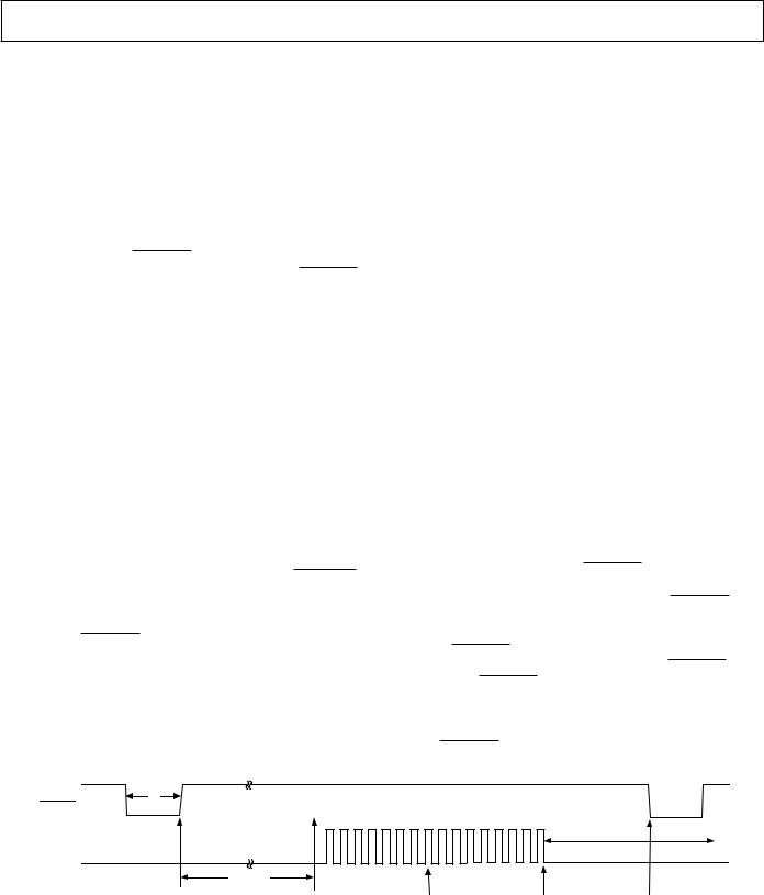
Figure 3 shows the timing and control sequence required to obtain optimum performance from the AD7893. In the sequence shown, conversion is initiated on the rising edge of CONVST, and new data from this conversion is available in the output register of the AD7893 6 μs later. Once the read operation has taken place, a further 600 ns should be allowed before the next rising edge of CONVST to optimize the settling of the track/ hold amplifier before the next conversion is initiated. With the serial clock frequency at its maximum of 8.33 MHz, the achievable throughput rate for the part is 6 μs (conversion time) plus 1.92 μs (read time) plus 0.6 μs (acquisition time). This results in a minimum throughput time of 8.52 μs (equivalent to a throughput rate of 117 kHz).
t1
CONVST
The read operation consists of sixteen serial clock pulses to the output shift register of the AD7893. After sixteen serial clock pulses the shift register is reset and the SDATA line is threestated. If there are more serial clock pulses after the sixteenth clock, the shift register will be moved on past its reset state; however, the shift register will be reset again on the falling edge of the CONVST signal to ensure that the part returns to a known state every conversion cycle. As a result, a read operation from the output register should not straddle across the falling edge of CONVST as the output shift register will be reset in the middle of the read operation, and the data read back into the microprocessor will appear invalid.
The throughput rate of the part can be increased by reading data during conversion. If the data is read during conversion, a throughput time of 6 μs (conversion time) plus 1.5 μs is achieved. This minimum throughput time of 7.5 μs is achieved with a slight reduction in performance from the AD7893. The signal to (noise + distortion) number is likely to degrade by ap-
proximately 1.5 dB while the code flicker from the part will also increase (see AD7893 PERFORMANCE section).
Because the AD7893 is provided in an 8-pin package to minimize board space, the number of pins available for interfacing is very limited. As a result, no status signal is provided from the AD7893 to indicate when conversion is complete. In many applications, this will not be a problem as the data can be read from the AD7893 during conversion or after conversion; however, applications that want to achieve optimum performance from the AD7893 will have to ensure that the data read does not occur during conversion or during 600 ns prior to the rising edge of CONVST. This can be achieved in two ways. The first is to ensure in software that the read operation is not initiated until 6 μs after the rising edge of CONVST. This will only be possible if the software knows when the CONVST command is issued. The second scheme would be to use the CONVST signal as both the conversion start signal and an interrupt signal. The simplest way to do this would be to generate a square wave signal for CONVST with high and low times of 6 μs (see Figure 4). Conversion is initiated on the rising edge of CONVST. The falling edge of CONVST occurs 6 μs later and can be used as either an active low or falling, edge-triggered interrupt signal to tell the processor to read the data from the AD7893. Provided that the read operation is completed 600 ns before the rising edge of CONVST, the AD7893 will operate to specification.
SCLK |
600ns MIN |
|
tCONVERT |
CONVERSION IS INITIATED |
CONVERSION ENDS |
SERIAL READ |
READ OPERATION |
OUTPUT SERIAL |
AND TRACK/HOLD GOES |
6µs LATER |
OPERATION |
SHOULD END 600ns |
SHIFT REGISTER IS |
INTO HOLD |
|
|
PRIOR TO NEXT |
RESET |
|
|
|
RISING EDGE OF |
|
|
|
|
CONVST |
|
Figure 3. Timing Sequence for Optimum Performance from the AD7893
REV. E |
–7– |
AD7893
CONVST
|
|
|
|
|
|
|
|
|
|
|
|
|
|
|
|
|
|
|
|
|
|
|
|
|
|
|
|
|
|
|
|
|
|
|
|
|
|
|
|
|
|
|
|
|
|
|
|
|
|
|
|
|
|
|
|
|
|
|
|
|
|
|
|
|
|
|
|
|
|
|
|
|
|
|
|
|
|
|
|
|
|
|
|
|
|
|
|
|
|
|
|
|
|
|
|
|
|
|
|
|
|
|
|
|
|
|
|
|
|
|
|
|
|
|
|
|
|
|
|
|
|
|
|
|
|
|
|
|
|
|
|
|
|
|
|
|
|
|
|
|
|
|
|
|
|
|
|
|
|
|
|
|
|
|
|
|
|
|
|
|
|
|
|
|
|
|
|
|
|
|
|
|
|
|
|
|
|
|
|
|
|
|
|
|
|
|
|
|
|
|
|
|
|
|
|
|
|
|
|
|
|
|
|
|
|
|
|
|
|
|
|
|
|
|
|
|
|
|
|
|
|
|
|
|
|
|
|
|
|
|
|
|
|
|
|
|
|
|
|
|
|
|
|
|
|
|
|
|
|
|
|
|
|
|
|
|
|
|
|
|
|
|
|
|
|
|
|
|
|
|
|
|
|
|
|
|
|
|
|
|
|
|
|
|
|
|
|
|
|
|
|
|
|
|
|
|
|
|
|
|
|
|
|
|
|
|
|
|
|
|
|
|
|
|
|
|
|
RISING EDGE OF |
||||||||||
|
|
|
|
|
|
COMPLETE |
|
|
|
|
|
|
|
|
|
|
|
|
|
|
|
|
|
|
|
|
|
|
|
|
|
|
||||||||||||||
|
|
|
|
|
|
|
|
|
|
|
|
|
|
|
|
|
|
|
|
|
|
|
|
|
|
|
|
|
|
|
|
|
|
|
|
|
|
|
|
CONVST |
||||||
SCLK |
|
|
|
|
|
|
|
|
|
|
|
|
|
|
|
|
|
|
|
|
|
|
|
|
|
|
|
|
|
|
|
|
|
|
|
|
|
|
|
|
600ns MIN |
|||||
|
|
|
|
tCONVERT |
|
|
|
|
|
|
|
|
|
|
|
|
|
|
|
|
|
|
|
|
|
|
|
|
|
|
|
|
|
|
|
|
|
|
|
|
|
|||||
CONVERSION IS INITIATED |
|
|
CONVST INDICATES |
µP INT SERVICE |
|
|
|
|
|
SERIAL READ |
|
|
READ OPERATION |
|||||||||||||||||||||||||||||||||
AND TRACK/HOLD GOES |
|
|
TO µP THAT |
OR POLLING |
|
|
|
|
|
OPERATION |
|
|
SHOULD END 600ns |
|||||||||||||||||||||||||||||||||
|
INTO HOLD |
|
|
CONVERSION IS |
ROUTINE |
|
|
|
|
|
|
|
|
|
|
|
|
|
|
|
|
|
|
|
|
|
PRIOR TO NEXT |
|||||||||||||||||||
|
|
|
|
|
|
|
|
|
|
|
|
|
|
|
|
|
|
|
|
|
|
|
|
|
|
|
|
|
|
|
|
|
|
|
|
|
|
|
|
|
|
|
||||
Figure 4. CONVST Used as Status Signal
This scheme limits the throughput rate to 12 μs minimum; however, depending on the response time of the microprocessor to the interrupt signal and the time taken by the processor to read the data, this may be the fastest the system could have operated. In any case, the CONVST signal does not have to have a 50:50 duty cycle. This can be tailored to optimize the throughput rate of the part for a given system.
Alternatively, the CONVST signal can be used as a normal narrow pulse width. The rising edge of CONVST can be used as an active high or rising edge-triggered interrupt. A software delay of 6 μs can then be implemented before data is read from the part.
Serial Interface
The serial interface to the AD7893 consists of just two wires, a serial clock input (SCLK) and the serial data output (SDATA). This allows for an easy to use interface to most microcontrollers, DSP processors and shift registers.
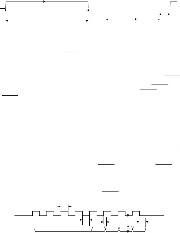
Figure 5 shows the timing diagram for the read operation to the AD7893. The serial clock input (SCLK) provides the clock source for the serial interface. Serial data is clocked out from the SDATA line on the rising edge of this clock and is valid on the falling edge of SCLK. Sixteen clock pulses must be provided to the part to access to full conversion result. The AD7893 provides four leading zeros followed by the 12-bit conversion result starting with the MSB (DB11). The last data bit to be clocked out on the final rising clock edge is the LSB (DB0). On the sixteenth falling edge of SCLK, the SDATA line is disabled (threestated). After this last bit has been clocked out, the SCLK input should return low and remain low until the next serial data read operation. If there are extra clock pulses after the sixteenth
t2
SCLK (I)
THREE-STATE
SDATA (O) |
|
FOUR LEADING ZEROS |
|
clock, the AD7893 will start over again with outputting data from its output register, and the data bus will no longer be three-stated even when the clock stops. Provided that the serial clock has stopped before the next falling edge of CONVST, the AD7893 will continue to operate correctly with the output shift register being reset on the falling edge of CONVST; however, the SCLK line must be low when CONVST goes low in order to reset the output shift register correctly.
The serial clock input does not have to be continuous during the serial read operation. The sixteen bits of data (four leading zeros and 12 bit conversion result) can be read from the AD7893 in a number of bytes; however, the SCLR input must remain low between the two bytes.
Normally, the output register is updated at the end of conversion. If a serial read from the output register is in progress when conversion is complete; however, the updating of the output register is deferred. In this case, the output register is updated when the serial read is completed. If the serial read has not been completed before the next falling edge of CONVST, the output register will be updated on the falling edge of CONVST, and the output shift register count is reset. In applications where the data read has been started and not completed before the falling edge of CONVST, the user must provide a CONVST pulse width of greater than 1.5 μs to ensure correct setup of the AD7893 before the next conversion is initiated. In applications where the output update takes place either at the end of conversion or at the end of a serial read that is completed 1.5 μs before the rising edge of CONVST, the normal pulse width of 50 ns minimum applies to CONVST.
t3 |
t4 |
t5 |
DB11 |
DB10 |
THREE-STATE |
DB0 |
Figure 5. Data Read Operation
–8– |
REV. E |

AD7893
The AD7893 counts the serial clock edges to know which bit from the output register should be placed on the SDATA output. To ensure that the part does not lose synchronization, the serial clock counter is reset on the falling edge of the CONVST input, provided the SCLR line is low. The user should ensure that a falling edge on the CONVST input does not occur while a serial data read operation is in progress.
MICROPROCESSOR/MICROCONTROLLER INTERFACE
The AD7893 provides a two-wire serial interface that can be used for connection to the serial ports of DSP processors and microcontrollers. Figures 6 through 9 show the AD7893 interfaced to a number of different microcontrollers and DSP processors. The AD7893 accepts an external serial clock and, as a result, in all interfaces shown here, the processor/controller is configured as the master, providing the serial clock with the AD7893 configured as the slave in the system.
AD7893-8051 Interface
Figure 6 shows an interface between the AD7893 and the 8XC51 microcontroller. The 8XC51 is configured for its Mode 0 serial interface mode. The diagram shows the simplest form of the interface where the AD7893 is the only part connected to the serial port of the 8XC51 and, therefore, no decoding of the serial read operations is required. It also makes no provisions for monitoring when conversion is complete on the AD7893.
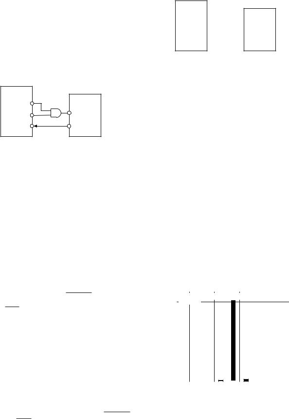
Either of these two tasks can readily be accomplished with minor modifications to the interface. To chip select the AD7893 in systems where more than one device is connected to the 8XC51’s serial port, a port bit configured as an output from one of the 8XC51’s parallel ports can be used to gate on or off the serial clock to the AD7893. A simple AND function on this port bit and the serial clock from the 8XC51 will provide this function. The port bit should be high to select the AD7893 and low when it is not selected.
To monitor the conversion time on the AD7893, a scheme such as previously outlined with CONVST can be used. This can be implemented in two ways. One is to connect the CONVST line to another parallel port bit that is configured as an input. This port bit can then be polled to determine when conversion is complete. An alternative is to use an interrupt driven system, in which case the CONVST line should be connected to the INT1 input of the 8XC51.
8XC51 |
AD7893 |
P3.0 
 SDATA
SDATA
P3.1 

 SCLK
SCLK
The serial clock rate from the 8XC51 is limited to significantly less than the allowable input serial clock frequency with which the AD7893 can operate. As a result, the time to read data from the part will actually be longer than the conversion time of the part. This means that the AD7893 cannot run at its maximum throughput rate when used with the 8XC51.
AD7893-68HC11 Interface
An interface circuit between the AD7893 and the 68HC11 microcontroller is shown in Figure 7. For the interface shown, the 68HC11 SPI port is used, and the 68HC11 is configured in its single-chip mode. The 68HC11 is configured in the master mode with its CPOL bit set to a logic zero and its CPHA bit set to a logic one. As with the previous interface, the diagram shows the simplest form of the interface where the AD7893 is the only part connected to the serial port of the 68HC11 and, therefore, no decoding of the serial read operations is required. It also makes no provisions for monitoring when conversion is complete on the AD7893.
Once again, either of these two tasks can readily be accomplished with minor modifications to the interface. To chip select the AD7893 in systems where more than one device is connected to the 68HC11’s serial port, a port bit, configured as an output from one of the 68HC11’s parallel ports, can be used to gate on or off the serial clock to the AD7893. A simple AND function on this port bit and the serial clock from the 68HC11 will provide this function. The port bit should be high to select the AD7893 and low when it is not selected.
To monitor the conversion time on the AD7893, a scheme such as outlined in the previous interface with CONVST can be used. This can be implemented in two ways. One is to connect the CONVST line to another parallel port bit that is configured as an input. This port bit can then be polled to determine when conversion is complete. An alternative is to use an interrupt driven system, in which case the CONVST line should be connected to the IRQ input of the 68HC11.
The serial clock rate from the 68HC11 is limited to significantly less than the allowable input serial clock frequency with which the AD7893 can operate. As a result, the time to read data from the part will actually be longer than the conversion time of the part. This means that the AD7893 cannot run at its maximum throughput rate when used with the 68HC11.
68HC11 |
AD7893 |
SCK
 SCLK
SCLK
MISO
 SDATA
SDATA
Figure 7. AD7893 to 68HC11 Interface
Figure 6. AD7893 to 8XC51 Interface
REV. E |
–9– |
AD7893
AD7893–ADSP-2105 Interface
An interface circuit between the AD7893 and the ADSP-2105 DSP processor is shown in Figure 8. In the interface shown, the RFS1 output from the ADSP-2105’s SPORT1 serial port is used to gate the serial clock (SCLK1) of the ADSP-2105 before it is applied to the SCLK input of the AD7893. The RFS1 output is configured for active high operation. The interface ensures a noncontinuous clock for the AD7893’s serial clock input with only sixteen serial clock pulses provided, and the serial clock line of the AD7893 remaining low between data transfers. The SDATA line from the AD7893 is connected to the DR1 line of the ADSP-2105’s serial port.
ADSP-2105
RFS1 |
AD7893 |
|
|
SCLK1 |
SCLK |
|
|
DR1 |
SDATA |
Figure 8. AD7893 to ADSP-2105 Interface
The timing relationship between the SCLK1 and RFS1 outputs of the ADSP-2105 are such that the delay between the rising edge of the SCLK1 and the rising edge of an active high RFS1 is up to 25 ns. There is also a requirement that data must be set up 10 ns prior to the falling edge of the SCLK1 to be read correctly by the ADSP-2105. The data access time for the AD7893 is 50 ns from the rising edge of its SCLK input. Assuming a
10 ns propagation delay through the external AND gate, the high time of the SCLK1 output of the ADSP-2105 must be ³ (50 + 25 + 10 + 10) ns, i.e., ³ 95 ns. This means that the serial clock frequency with which the interface of Figure 13 can work with is limited to 5.26 MHz.
An alternative scheme is to configure the ADSP-2105 to accept an external serial clock. In this case, an external noncontinuous serial clock that drives the serial clock inputs of both the ADSP2105 and the AD7893 is provided. In this scheme, the serial clock frequency is limited to 5 MHz by the ADSP-2105.
To monitor the conversion time on the AD7893, a scheme such as outlined in previous interfaces with CONVST can be used. This can be implemented by connecting the CONVST line directly to the IRQ2 input of the ADSP-2105.
AD7893–DSP56000 Interface
Figure 9 shows an interface circuit between the AD7893 and the DSP56000 DSP processor. The DSP5600 is configured for normal mode asynchronous operation with gated clock. It is also set up for a 16-bit word with the gated serial clock being generated by the DSP56000 and appears on the SC0 pin. The SC0 pin should be configured as an output by setting bit SCD0 to 1. In this mode, the DSP56000 provides sixteen serial clock pulses to the AD7893 in a serial read operation. The DSP56000 assumes valid data on the first falling edge of SCK, so the interface is simply two-wire as shown in Figure 9.
To monitor the conversion time on the AD7893, a scheme such as outlined in previous interface examples with CONVST can be used. This can be implemented by connecting the CONVST line directly to the IRQA input of the DSP56000.
DSP56000
AD7893
SRD 
 SDATA
SDATA
SC0
 SCLK
SCLK
Figure 9. AD7893 to DSP56000 Interface
AD7893 PERFORMANCE Linearity
The linearity of the AD7893 is determined by the on-chip 12-bit D/A converter. This is a segmented DAC that is laser trimmed for 12-bit integral linearity and differential linearity. Typical relative numbers for the part are ±1/4 LSB, while the typical DNL errors are ±1/2 LSB.
Noise
In an A/D converter, noise exhibits itself as code uncertainty in dc applications and as the noise floor (in an FFT, for example) in ac applications. In a sampling A/D converter like the AD7893, all information about the analog input appears in the baseband from dc to 1/2 the sampling frequency. The input bandwidth of the track/hold exceeds the Nyquist bandwidth; therefore, an antialiasing filter should be used to remove unwanted signals above fS/2 in the input signal in applications where such signals exist.
Figure 10 shows a histogram plot for 8192 conversions of a dc input using the AD7893. The analog input was set at the center of a code transition. The timing and control sequence used was per Figure 3 where the optimum performance of the ADC was achieved. It can be seen that almost all the codes appear in the one output bin, indicating very good noise performance from the ADC. The rms noise performance for the AD7893-2 for the above plot was 87 mV. Since the analog input range, and hence LSB size, on the AD7893-10 is eight times what it is for the AD7893-2, the same output code distribution results in an output rms noise of 700 mV for the AD7893-10.
|
9000 |
|
|
|
|
|
|
|
|
|
SAMPLING |
FREQUENCY = |
102.4kHz |
|
|
|
|||
|
|
|
|
|
|||||
|
8000 |
TA = +25°C |
|
|
|
|
|
|
|
|
|
|
|
|
|
|
|
||
|
|
|
|
|
|
|
|
|
|
CODE |
7000 |
|
|
|
|
|
|
|
|
|
|
|
|
|
|
|
|
||
6000 |
|
|
|
|
|
|
|
|
|
|
|
|
|
|
|
|
|
||
OF |
5000 |
|
|
|
|
|
|
|
|
OCCURRENCES |
|
|
|
|
|
|
|
|
|
4000 |
|
|
|
|
|
|
|
|
|
|
|
|
|
|
|
|
|
|
|
|
3000 |
|
|
|
|
|
|
|
|
|
|
|
|
|
|
|
|
|
|
|
2000 |
|
|
|
|
|
|
|
|
|
|
|
|
|
|
|
|
|
|
|
1000 |
|
|
|
|
|
|
|
|
|
|
|
|
|
|
|
|
|
|
|
0 |
|
|
|
|
|
|
|
|
|
(X–4) (X–3) (X–2) (X–1) X (X+1) (X+2) (X+3) (X+4) |
||||||||
|
|
||||||||
|
|
|
|
CODE |
|||||
Figure 10. Histogram of 8192 Conversions of a DC Input
–10– |
REV. E |