

бакМИТ_КП2015 / Компоненты по вариантам / АЦП / AD7893-5
.pdfThe same data is presented in Figure 11 as in Figure 10 except that, in this case, the output data read for the device occurs during conversion. This has the effect of injecting noise onto the die while bit decisions are being made; this increases the noise generated by the AD7893. The histogram plot for 8192 conversions of the same dc input now shows a larger spread of codes with the rms noise for the AD7893-2 increasing to 210 μV. This effect will vary depending on where the serial clock edges appear with respect to the bit trials of the conversion process. It is possible to achieve the same level of performance when reading during conversion as when reading after conversion, depending on the relationship of the serial dock edges to the bit trial points.
|
7500 |
|
|
|
|
|
|
|
|
|
|
|
|
|
|
|
|
|
|
|
|
|
|
|
|
|
7000 |
SAMPLING |
|
|
|
|
|
|
|
|
|
|
|
6500 |
FREQUENCY |
= 102.4kHz |
|
|
|
|
|
|
|
|
|
|
TA = +25°C |
|
|
|
|
|
|
|
|
|
|
|
CODE |
6000 |
|
|
|
|
|
|
|
|
|
|
|
5000 |
|
|
|
|
|
|
|
|
|
|
|
|
OF |
5500 |
|
|
|
|
|
|
|
|
|
|
|
4500 |
|
|
|
|
|
|
|
|
|
|
|
|
OCCURRENCES |
|
|
|
|
|
|
|
|
|
|
|
|
4000 |
|
|
|
|
|
|
|
|
|
|
|
|
|
|
|
|
|
|
|
|
|
|
|
|
|
|
3500 |
|
|
|
|
|
|
|
|
|
|
|
|
|
|
|
|
|
|
|
|
|
|
|
|
|
3000 |
|
|
|
|
|
|
|
|
|
|
|
|
|
|
|
|
|
|
|
|
|
|
|
|
|
2500 |
|
|
|
|
|
|
|
|
|
|
|
|
|
|
|
|
|
|
|
|
|
|
|
|
|
2000 |
|
|
|
|
|
|
|
|
|
|
|
|
|
|
|
|
|
|
|
|
|
|
|
|
|
1500 |
|
|
|
|
|
|
|
|
|
|
|
|
|
|
|
|
|
|
|
|
|
|
|
|
|
1000 |
|
|
|
|
|
|
|
|
|
|
|
|
|
|
|
|
|
|
|
|
|
|
|
|
|
500 |
|
|
|
|
|
|
|
|
|
|
|
|
|
|
|
|
|
|
|
|
|
|
|
|
|
0 |
|
|
|
|
|
|
|
|
|
|
|
|
(X–4) (X–3) (X–2) (X–1) X (X+1) (X+2) (X+3) (X+4) |
|||||||||||
|
|
|||||||||||
|
|
|
|
CODE |
||||||||
Figure 11. Histogram of 8192 Conversions with Read During Conversion
Dynamic Performance
With a combined conversion and acquisition time of 7.5 μs, the AD7893 is ideal for wide bandwidth signal processing applications. These applications require information on the ADC’s effect on the spectral content of the input signal. Signal to (noise + distortion) ratio, total harmonic distortion, peak harmonic or spurious noise, and intermodulation distortion are all specified. Figure 12 shows a typical FFT plot of a 10 kHz, 0 V to +2.5 V input after being digitized by the AD7893-2, operating at a 102.4 kHz sampling rate. The signal to (noise + distortion) ratio is 71.5 dB, and the total harmonic distortion is –83 dB.
|
0 |
|
|
|
|
SAMPLE RATE = 102.4kHz |
|
|
|
INPUT FREQUENCY = 10kHz |
|
|
|
SNR = 71.5dB |
|
|
–30 |
TA = +25°C |
|
– dB |
–60 |
|
|
SIGNAL AMPLITUDE |
|
|
|
–80 |
|
|
|
–120 |
|
|
|
|
|
|
|
|
–180 |
25.6 |
51.2 |
|
0 |
FREQUENCY – kHz
SNR IS SIGNAL TO (NOISE AND DISTORTION) RATIO
Figure 12. AD7893 FFT Plot
AD7893
Effective Number of Bits
The formula for signal to (noise + distortion) ratio (see Terminology section) is related to the resolution or number of bits in the converter. Rewriting the formula gives a measure of performance expressed in effective number of bits (N):
N = (SNR – 1.76) / 6.02
where SNR is Signal to (Noise + Distortion) Ratio.
The effective number of bits for a device can be calculated from its measured signal to (noise + distortion) ratio. Figure 13 shows a typical plot of effective number of bits versus frequency for the
AD7893-2 from dc to fSAMPLING/2. The sampling frequency is 102.4 kHz. The plot shows that the AD7893 converts an input
sine wave of 51.2 kHz to an effective numbers of bits of 11, which equates to a signal to (noise + distortion) level of 68 dB.
|
12.0 |
BITSOF |
11.5 |
NUMBER |
11.0 |
EFFECTIVE |
10.5 |
|
|
|
10.0 |
0 |
25.6 |
51.2 |
|
INPUT FREQUENCY – kHz |
|
Figure 13. Effective Number of Bits vs. Frequency
REV. E |
–11– |
AD7893
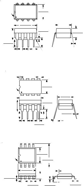
OUTLINE DIMENSIONS
Dimensions shown in inches and (mm).
Plastic DIP (N-8)
8 |
|
5 |
|
|
PIN 1 |
|
0.280 (7.11) |
|
|
|
0.240 (6.10) |
|
||
|
|
|
||
1 |
|
4 |
|
|
0.430 (10.92) |
|
0.325 (8.25) |
||
|
0.348 (8.84) |
|
|
0.300 (7.62) |
0.210 |
|
0.060 (1.52) |
0.195 (4.95) |
|
|
0.015 (0.38) |
|||
(5.33) |
|
0.115 (2.93) |
||
|
|
|
||
MAX |
|
|
|
|
0.160 (4.06) |
|
|
0.130 |
0.015 (0.381) |
|
|
(3.30) |
||
0.115 (2.93) |
|
|
MIN |
0.008 (0.204) |
0.022 (0.558) |
0.100 |
0.070 (1.77) |
SEATING |
|
PLANE |
|
|||
0.014 (0.356) |
(2.54) |
0.045 (1.15) |
|
|
|
|
|||
|
BSC |
|
|
|
Cerdip (Q-8)
0.005 (0.13) MIN |
0.055 (1.4) MAX |
|
|
|
8 |
|
5 |
|
|
PIN 1 |
|
0.310 (7.87) |
|
|
|
0.220 (5.59) |
|
||
|
|
|
||
1 |
|
4 |
|
|
|
|
|
|
0.320 (8.13) |
0.405 (10.29) MAX |
|
0.290 (7.37) |
||
0.200 |
|
0.060 (1.52) |
|
|
|
0.015 (0.38) |
|
||
(5.08) |
|
|
||
|
|
|
|
|
MAX |
|
|
|
|
|
|
|
0.150 |
0.015 (0.38) |
0.200 (5.08) |
|
|
(3.81) |
|
|
|
0.008 (0.20) |
||
0.125 (3.18) |
|
|
MIN |
|
|
|
15° |
||
|
|
|
||
|
|
|
|
|
0.023 (0.58) |
0.100 |
0.070 (1.78) |
SEATING |
0° |
0.014 (0.36) |
(2.54) |
0.030 (0.76) |
|
|
|
BSC |
|
PLANE |
|
SOIC (SO-8)
8 |
5 |
|
|
|
|
0.1574 (4.00) |
|
PIN 1 |
|
0.1497 (3.80) |
|
4 |
0.2440 (6.20) |
||
1 |
|||
|
|
0.2284 (5.80) |
|
0.1968 (5.00) |
|
|
|
0.1890 (4.80) |
|
|
|
0.0098 (0.25) |
|
0.0688 (1.75) |
|
|
0.0532 (1.35) |
||
0.0040 (0.10) |
|
||
|
|
|
|
|
|
|
|
|
|
|
|
0.0500 |
0.0192 (0.49) |
0.0098 (0.25) |
|||||||
(1.27) |
|
0.0138 (0.35) |
0.0075 (0.19) |
||||||
BSC |
|||||||||
|
|
|
|
|
|
||||
|
|
0.0196 (0.50) |
|
|
|
||
|
|
0.0099 (0.25) x 45 ° |
|||||
8° |
|||||||
|
|
|
|
|
|||
|
|
|
|
|
|||
0° |
0.0500 (1.27) |
||||||
|
|
0.0160 (0.41) |
|||||
C1787c–2–1/97
PRINTED IN U.S.A.
–12– |
REV. E |