


ADS8326
SBAS343C –MAY 2007 –REVISED SEPTEMBER 2009 |
www.ti.com |
TIMING INFORMATION
tCYC
CS/SHDN
Power Down
 Sample

 Conversion
tSUCS
DCLOCK
tCSD |
Use positive clock edge for data transfer |
|
DOUT |
Hi-Z |
0 B15 B14 B13 B12 B11 B10 |
B9 B8 B7 B6 B5 B4 B3 B2 B1 B0(1) |
Hi-Z |
|
|
|
(MSB) |
(LSB) |
|
|
|
tSMPL |
|
|
|
|
|
|
tCONV |
|
|
|
NOTE: (1) A minimum of 22 clock cycles are required for 16-bit conversion; 24 clock cycles are shown.
If CS remains low at the end of conversion, a new data stream is shifted out with LSB-first data followed by zeroes indefinitely.
|
|
|
|
|
|
|
|
|
|
|
|
|
|
|
|
|
|
|
|
|
|
|
|
|
|
|
|
|
|
tCYC |
|
|
|
|
|
|
|
|
|
|
|
|
|
|
|
|
|
|
|
|
|
|
||||
|
|
|
|
|
|
|
|
|
|
|
|
|
|
|
|
|
|
|
|
|
|
|
|
|
|
|
|
|
|
|
|
|
|
|
|
|
|
|
|
|
|
|
|
|
|
|
|
|
|
|
|
|
|
|
|
|
CS/SHDN |
|
|
|
|
|
|
|
|
|
|
|
|
|
|
|
|
|
|
|
|
|
|
|
|
|
|
|
|
|
|
|
|
|
|
|
|
|
|
|
|
|
|
|
|
|
|
|
|
|
|
|
|
|
|
|
|
|
|
|
|
|
|
|
|
|
|
|
|
|
|
|
|
|
|
|
|
|
|
|
|
|
|
|
|
|
|
|
|
|
|
|
|
|
|
|
|
|
|
|
|
|
|
|
|
|
|
|
|
|
|
|
|
|
|
|
|
|
|
tSUCS |
|
|
|
|
|
|
|
|
|
|
|
|
|
|
|
|
|
|
|
|
|
|
|
|
|
|
Power Down |
|
|||||||||||||||||||||||
|
|
|
|
|
|
|
|
|
|
|
|
|
|
|
|
|
|
|
|
|
|
|
|
|
|
|
|
|
|
|
|
|||||||||||||||||||||||||
DCLOCK |
|
|
|
|
|
|
|
|
|
|
|
|
|
|
|
|
|
|
|
|
|
|
|
|
|
|
|
|
|
|
|
|
|
|
|
|
|
|
|
|
|
|
|
|
|
|
|
|
|
|
|
|
|
|
|
|
|
|
|
|
|
|
|
|
|
|
|
|
|
|
|
|
|
|
|
|
|
|
|
|
|
|
|
|
|
|
|
|
|
|
|
|
|
|
|
|
|
|
|
|
|
|
|
|
|
|
|
|
|
|
|
||
|
|
|
|
|
|
|
|
|
|
|
|
|
|
|
|
|
|
|
|
|
|
|
|
|
|
|
|
|
|
|
|
|
|
|
|
|
|
|
|
|
|
|
|
|
|
|
|
|
|
|
|
|
|
|
|
|
|
|
|
|
tCSD |
|
|
|
|
|
|
|
|
|
|
|
|
|
|
|
|
|
|
|
|
|
|
|
|
|
|
|
|
|
|
|
|
|
|
|
|
|
|
|
|
||||||||||||
|
|
|
|
|
|
|
|
|
|
|
|
|
|
|
|
|
|
|
|
|
|
|
|
|
|
|
|
|
|
|
|
|
|
|
|
|
|
|
|
|
|
|||||||||||||||
|
DOUT |
|
|
Hi-Z |
B15 |
B14 |
B6 |
B5 |
B4 |
B3 |
B2 |
B1 |
B0 B1 |
B2 |
B3 |
B4 |
B5 |
B0 |
B11 |
B12 |
B13 |
B14 |
(2) |
Hi-Z |
|
|||||||||||||||||||||||||||||||
|
|
|
|
|
|
|
|
|
|
|
|
0 |
B15 |
|
|
|||||||||||||||||||||||||||||||||||||||||
|
|
|
|
|
|
|
|
|
|
|
|
|
|
|
|
|
|
|
|
|
|
|
|
|
|
|
|
|
|
|
|
|
|
|
|
|
|
|
|
|
|
|
|
|
|
|
|
|
|
|
|
|
|
|
|
|
|
|
|
|
|
|
|
tSMPL |
|
|
(MSB) |
|
tCONV |
(LSB) |
|
|
|
|
|
|
|
|
|
|
|
|
|
|
|
|
|
(MSB) |
|
||||||||||||||||||||||||
|
|
|
|
|
|
|
|
|
|
|
|
|
|
|
|
|
|
|
|
|
|
|
|
|
|
|
|
|
|
|
|
|
|
|
|
|
|
|
|
|||||||||||||||||
|
|
|
|
|
|
|
|
|
|
|
|
|
|
|
|
|
|
|
|
|
|
|
|
|
|
|
|
|
|
|
|
|
|
|
|
|
|
|
|
|
|
|
|
|
|
|
|
|
|
|
|
|
|
|
|
|
NOTE: (2) After completing the data transfer, if further clocks are applied with CS low, the A/D converter will output zeroes indefinitely.
|
|
|
1.4V |
|
|
|
|
|
|
|
|
|
|
|
|
|
|
|
|
|
|
|
|
|
|
|
|
|||||
|
|
|
|
|
|
|
|
|
3kΩ |
|
|
|
|
|
|
|
|
|
|
|
|
|
90% |
|||||||||
|
|
|
|
|
|
|
|
|
|
|
|
|
|
|
|
|
|
|
|
|
|
|||||||||||
|
|
|
|
|
|
|
|
|
|
|
||||||||||||||||||||||
|
|
|
|
|
|
|
|
|
|
|
|
DOUT |
|
|
|
|
|
|
|
|
|
|
|
|
|
|
||||||
|
DOUT |
|
|
|
|
|
|
|
|
|
Test Point |
|
|
|
|
|
|
|
|
|
|
|
|
|
|
|
|
|
|
10% |
||
|
|
|
|
|
|
|
|
|
|
|
|
|
|
|
|
|
|
|
|
|
|
|
|
|
|
|
|
|||||
|
|
|
|
|
|
|
|
|
|
|
|
|
|
|
|
|
|
|
|
|
|
|
|
|||||||||
|
|
|
|
|
|
|
|
|
|
|
||||||||||||||||||||||
|
|
|
|
|
|
|
|
|
|
|
|
tr |
|
|
|
|
|
|
|
|
|
|
|
|
|
|
|
|
|
|
tf |
|
|
|
|
|
|
|
|
|
|
100pF |
|
|
|
|
|
|
|
|
|
|
|
|
|
|
|
|
|
|
|
||||
|
|
|
|
|
|
|
|
|
CLOAD |
|
||||||||||||||||||||||
|
|
|
|
|
|
|
|
|
|
|
|
Voltage Waveforms for DOUT Rise and Fall Times, tr, tf |
||||||||||||||||||||
|
|
|
|
|
|
|
|
|
||||||||||||||||||||||||
|
Load Circuit for tdDO, tr, and tf |
|
||||||||||||||||||||||||||||||
|
|
|
|
|
|
|
|
|
|
|
|
|
Test Point |
|
||||||||||||||||||
|
|
|
|
|
|
|
|
|
|
|
|
|
|
|
|
|
|
|
|
|
|
|
|
|
|
|
|
|
|
|
|
|
DCLOCK |
|
|
|
|
|
|
|
|
|
|
|
|
|
|
|
|
|
|
|
|
|
VDD |
|
|||||||||
|
|
|
|
|
|
|
|
|
|
|
|
|
|
|
|
|
|
|
|
|
|
|
|
|
||||||||
|
|
|
tdDO |
|
|
|
DOUT |
|
|
|
|
|
|
|
|
3kΩ |
|
|
tdis Waveform 2, ten |
|||||||||||||
|
|
|
|
|
|
|
|
|
|
|
|
|
|
|
||||||||||||||||||
|
|
|
|
|
|
|
|
|
|
|
|
|
|
|
|
|
|
|
|
|
|
|
|
|
tdis Waveform 1 |
|||||||
|
|
|
|
|
|
|
|
|
|
|
|
|
|
|
|
|
|
|
|
|
|
|
|
|
|
|
|
|
|
|
|
|
DOUT |
|
|
|
|
|
|
|
|
|
|
|
|
|
|
|
|
|
|
100pF |
|
||||||||||||
|
|
|
|
|
|
|
|
|
|
|
|
|
|
|
|
|
|
|
||||||||||||||
|
|
|
|
|
|
|
|
|
|
|
|
|
|
|
|
|
|
CLOAD |
|
|
|
|
|
|
|
|
|
|||||
|
thDO |
|
|
|
|
|
|
|
|
|
|
|
|
|
|
|
|
|
|
|
|
|
|
|
|
|
||||||
|
|
|
|
|
|
|
|
|
|
|
|
|
|
|
|
|
|
|
Load Circuit for tdis and ten |
|
||||||||||||
|
|
|
|
|
|
|
|
|
|
|
|
|
|
|
|
|
|
|
|
|||||||||||||
|
|
|
|
|
|
|
|
|
|
|
|
|
|
|
|
|
|
|
|
|
|
|||||||||||
|
Voltage Waveforms for DOUT Delay Times, tdDO |
|
||||||||||||||||||||||||||||||
CS/SHDN |
90% |
CS/SHDN |
|
|
|
|
|
|
|
|
|||
|
|
|
|
|
|
|
DOUT |
90% |
DCLOCK |
1 |
4 |
5 |
|
Waveform 1(3) |
|
|
|
|
||
|
|
|
|
|
||
|
|
tdis |
|
|
|
|
D |
OUT |
10% |
DOUT |
|
|
B15 |
Waveform 2(4) |
|
|
|
|
||
|
|
|
|
ten |
||
|
|
|
|
|
|
|
|
|
Voltage Waveforms for tdis |
|
|
Voltage Waveforms for ten |
|
|
|
|
|
|
||
NOTES: (3) Waveform 1 is for an output with internal conditions such that |
|
|
|
|
||
the output is high unless disabled by the output control. |
|
|
|
|
||
(4) Waveform 2 is for an output with internal conditions such that |
|
|
|
|
||
the output is low unless disabled by the output control. |
|
|
|
|
||
Figure 1. Timing Diagrams and Test Circuits for the Parameters in Table 1
8 |
Submit Documentation Feedback |
Copyright © 2007–2009, Texas Instruments Incorporated |
Product Folder Link(s): ADS8326

|
|
|
|
|
|
|
|
ADS8326 |
www.ti.com |
|
|
|
SBAS343C –MAY 2007–REVISED SEPTEMBER 2009 |
||||
|
|
|
TIMING INFORMATION (continued) |
|
|
|
||
|
|
|
Table 1. Timing Characteristics |
|
|
|
||
|
|
|
|
|
|
|
|
|
SYMBOL |
|
DESCRIPTION |
MIN |
|
TYP |
MAX |
UNIT |
|
|
|
|
|
|
|
|
|
|
tSMPL |
|
Analog input sample time |
4.5 |
|
|
5.0 |
DCLOCKs |
|
tCONV |
|
Conversion time |
|
|
16 |
|
DCLOCKs |
|
tCYC |
|
Complete cycle time |
22 |
|
|
|
DCLOCKs |
|
tCSD |
|
|
falling to DCLOCK low |
|
|
|
0 |
ns |
|
CS |
|
|
|
||||
tSUCS |
|
|
falling to DCLOCK rising |
20 |
|
|
|
ns |
|
CS |
|
|
|
||||
tHDO |
|
DCLOCK falling to current DOUT not valid |
5 |
|
15 |
|
ns |
|
tDIS |
|
|
rising to DOUT tri-state |
|
|
70 |
100 |
ns |
|
CS |
|
|
|||||
tEN |
|
DCLOCK falling to DOUT enabled |
|
|
20 |
50 |
ns |
|
tF |
|
DOUT fall time |
|
|
5 |
25 |
ns |
|
tR |
|
DOUT rise time |
|
|
7 |
25 |
ns |
|
Copyright © 2007–2009, Texas Instruments Incorporated |
Submit Documentation Feedback |
9 |
Product Folder Link(s): ADS8326
ADS8326
SBAS343C –MAY 2007 –REVISED SEPTEMBER 2009 |
www.ti.com |
ILE(LSB)
TYPICAL CHARACTERISTICS: VDD = +5V
At TA = +25°C, VDD = +5V, VREF = +5V. fSAMPLE = 250kHz, fCLK = 24 × fSAMPLE, unless otherwise noted.
|
|
INTEGRAL LINEARITY ERROR |
|
|
|
|
|
DIFFERENTIAL LINEARITY ERROR |
|
|
||||||||||
|
|
|
|
vs |
|
|
|
|
|
|
|
|
|
vs |
|
|
|
|
||
|
|
|
|
CODE |
|
|
|
|
|
|
|
|
|
CODE |
|
|
|
|
||
3 |
|
|
|
|
|
|
|
|
|
|
3 |
|
|
|
|
|
|
|
|
|
2 |
|
|
|
|
|
|
|
|
|
|
2 |
|
|
|
|
|
|
|
|
|
|
|
|
|
|
|
|
|
|
|
|
|
|
|
|
|
|
|
|
||
1 |
|
|
|
|
|
|
|
|
|
DLE(LSB) |
1 |
|
|
|
|
|
|
|
|
|
|
|
|
|
|
|
|
|
|
|
|
|
|
|
|
|
|
|
|||
0 |
|
|
|
|
|
|
|
|
|
0 |
|
|
|
|
|
|
|
|
|
|
|
|
|
|
|
|
|
|
|
|
|
|
|
|
|
|
|
|
|
||
−1 |
|
|
|
|
|
|
|
|
|
|
−1 |
|
|
|
|
|
|
|
|
|
|
|
|
|
|
|
|
|
|
|
|
|
|
|
|
|
|
|
|
||
−2 |
|
|
|
|
|
|
|
|
|
|
−2 |
|
|
|
|
|
|
|
|
|
|
|
|
|
|
|
|
|
|
|
|
|
|
|
|
|
|
|
|
||
−3 |
|
|
|
|
|
|
|
|
|
|
−3 |
|
|
|
|
|
|
|
|
|
|
|
|
|
|
|
|
|
|
|
|
|
|
|
|
|
|
|
|
||
0000h |
4000h |
8000h |
C000h |
FFFFh |
|
0000h |
4000h |
8000h |
C000h |
FFFFh |
||||||||||
|
|
|
|
Output Code |
|
|
|
|
|
|
|
|
|
Output Code |
|
|
|
|
||
|
|
|
|
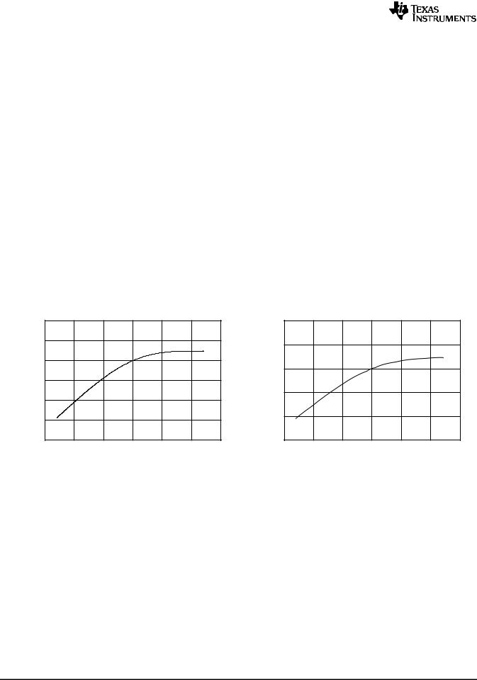
Figure 2. |
|
|
|
|
|
|
|
|
|
Figure 3. |
|
|
|
|
||
|
|
CHANGE IN OFFSET |
|
|
|
|
|
|
|
vs |
|
|
|
|
|
TEMPERATURE |
|
|
|
|
0.50 |
|
|
|
|
|
|
0.25 |
|
|
|
|
|
Deltafrom+25°C(LSB) |
Deltafrom+25°C(LSB) |
|
|
|
|
|
|
0 |
|
|
|
|
|
|
−0.25 |
|
|
|
|
|
|
−0.50 |
|
|
|
|
|
|
−0.75 |
|
|
|
|
|
|
−1.00 |
|
|
|
|
|
|
−50 |
−25 |
0 |
25 |
50 |
75 |
100 |
|
|
|
Temperature (°C) |
|
|
|
CHANGE IN GAIN vs TEMPERATURE
0.50
0.25
0
−0.25
−0.50
−0.75
−50 |
−25 |
0 |
25 |
50 |
75 |
100 |
Temperature (°C)
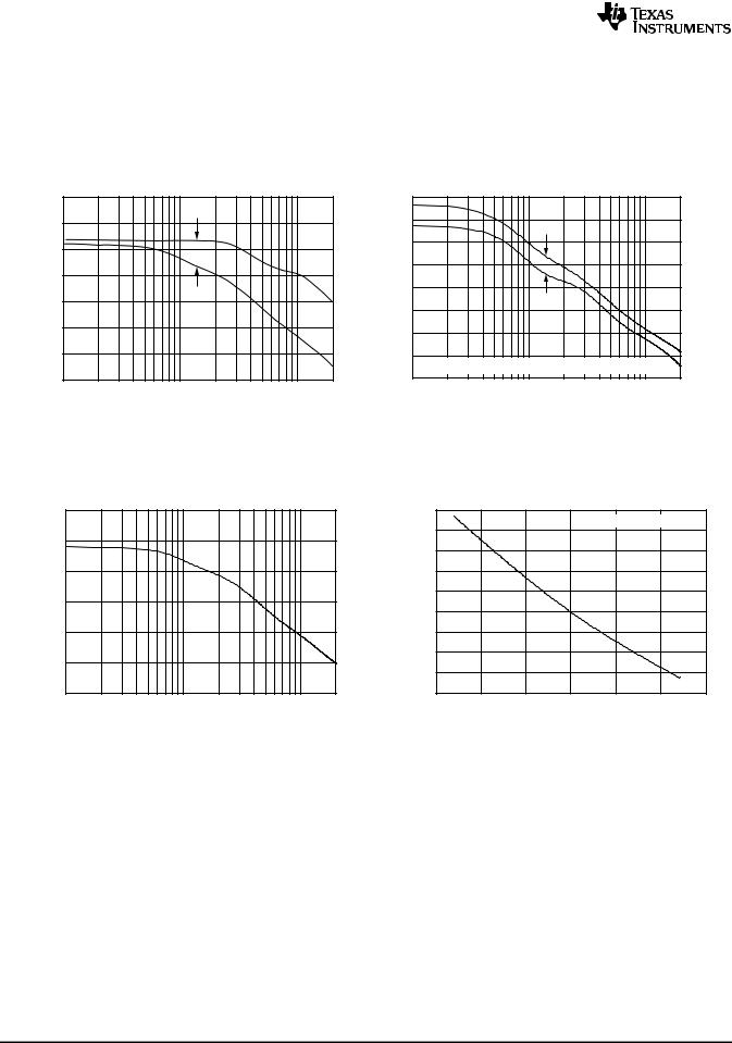
Figure 4. |
Figure 5. |
10 |
Submit Documentation Feedback |
Copyright © 2007–2009, Texas Instruments Incorporated |
Product Folder Link(s): ADS8326
ADS8326
www.ti.com |
SBAS343C –MAY 2007–REVISED SEPTEMBER 2009 |
TYPICAL CHARACTERISTICS: VDD = +5V (continued)
At TA = +25°C, VDD = +5V, VREF = +5V. fSAMPLE = 250kHz, fCLK = 24 × fSAMPLE, unless otherwise noted.
CHANGE IN OFFSET vs
COMMON-MODE VOLTAGE
|
30 |
|
|
|
|
|
|
|
|
(LSB) |
25 |
|
|
|
|
|
|
|
|
20 |
|
|
|
|
|
|
|
|
|
=0V |
|
|
|
|
|
|
|
|
|
15 |
|
|
|
|
|
|
|
|
|
CM |
|
|
|
|
|
|
|
|
|
|
|
|
|
|
|
|
|
|
|
V |
10 |
|
|
|
|
|
|
|
|
TO |
|
|
|
|
|
|
|
|
|
|
|
|
|
|
|
|
|
|
|
RELATIVE |
5 |
|
|
|
|
|
|
|
|
0 |
|
|
|
|
|
|
|
|
|
DELTA |
−5 |
|
|
|
|
|
|
|
|
|
−10 |
|
|
|
|
|
|
|
|
|
−0.5 |
−0.4 −0.3 −0.2 −0.1 |
0 |
0.1 |
0.2 |
0.3 |
0.4 |
0.5 |
0.6 |
VCM (V)
Figure 6.
FREQUENCY SPECTRUM
(8192 point FFT, fIN = 1.9836kHz, –0.2dB)
|
0 |
|
|
−20 |
|
Amplitude(dB) |
−40 |
|
−60 |
||
|
||
|
−80 |
−100
−120
−140
−160
0 |
25 |
50 |
75 |
100 |
125 |
Frequency (kHz)
CHANGE IN GAIN vs
COMMON-MODE VOLTAGE
|
30 |
|
|
|
|
|
|
|
|
(LSB) |
25 |
|
|
|
|
|
|
|
|
20 |
|
|
|
|
|
|
|
|
|
=0V |
|
|
|
|
|
|
|
|
|
15 |
|
|
|
|
|
|
|
|
|
CM |
|
|
|
|
|
|
|
|
|
|
|
|
|
|
|
|
|
|
|
V |
10 |
|
|
|
|
|
|
|
|
TO |
|
|
|
|
|
|
|
|
|
|
|
|
|
|
|
|
|
|
|
RELATIVE |
5 |
|
|
|
|
|
|
|
|
0 |
|
|
|
|
|
|
|
|
|
DELTA |
−5 |
|
|
|
|
|
|
|
|
|
−10 |
|
|
|
|
|
|
|
|
|
−0.5 |
−0.4 −0.3 −0.2 −0.1 |
0 |
0.1 |
0.2 |
0.3 |
0.4 |
0.5 |
0.6 |
VCM (V)
Figure 7.
FREQUENCY SPECTRUM
(8192 point FFT, fIN = 9.9792kHz, –0.2dB)
|
0 |
|
|
−20 |
|
Amplitude(dB) |
−40 |
|
−60 |
||
|
||
|
−80 |
|
|
−100 |
−120
−140
−160
0 |
25 |
50 |
75 |
100 |
125 |
Frequency (kHz)
Figure 8. |
Figure 9. |
Copyright © 2007–2009, Texas Instruments Incorporated |
Submit Documentation Feedback |
11 |
Product Folder Link(s): ADS8326
ADS8326
SBAS343C –MAY 2007 –REVISED SEPTEMBER 2009 |
www.ti.com |
TYPICAL CHARACTERISTICS: VDD = +5V (continued)
At TA = +25°C, VDD = +5V, VREF = +5V. fSAMPLE = 250kHz, fCLK = 24 × fSAMPLE, unless otherwise noted.
SNRandSINAD(dB)
SIGNAL-TO-NOISE AND |
SPURIOUS-FREE DYNAMIC RANGE AND |
SIGNAL-TO-NOISE + DISTORTION |
TOTAL HARMONIC DISTORTION |
vs |
vs |
INPUT FREQUENCY |
INPUT FREQUENCY |
100 |
|
|
|
|
105 |
|
|
−105 |
|
|
SNR |
|
|
|
100 |
|
|
−100 |
|
95 |
|
|
|
|
SFDR |
|
|
||
|
|
|
|
|
|
|
|
||
|
|
|
|
|
|
|
|
|
|
90 |
|
|
|
|
95 |
|
|
−95 |
|
|
|
|
|
|
|
|
|
|
|
|
|
|
|
SFDR(dB) |
90 |
|
|
−90 |
THD(dB) |
85 |
|
|
|
|
|
|
|
||
|
|
|
|
|
|
|
|
|
|
|
SINAD |
|
|
|
85 |
|
|
−85 |
|
80 |
|
|
|
|
THD(1) |
|
|
|
|
|
|
|
|
80 |
|
−80 |
|
||
|
|
|
|
|
|
|
|
||
75 |
|
|
|
|
75 |
|
|
−75 |
|
|
|
|
|
|
|
|
|
||
70 |
|
|
|
|
70 |
|
|
−70 |
|
|
|
|
|
|
|
NOTE: (1) First nine harmonics of the input frequency. |
|
|
|
65 |
|
|
|
|
65 |
|
|
−65 |
|
1 |
10 |
100 |
200 |
|
1 |
10 |
100 |
200 |
|
|
Frequency (kHz) |
|
|
|
|
Frequency (kHz) |
|
|
|
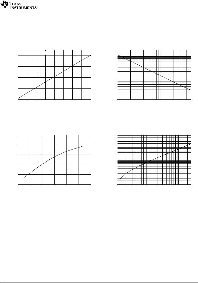
Figure 10. |
Figure 11. |
EFFECTIVE NUMBER OF BITS |
CHANGE IN SIGNAL-TO-NOISE + DISTORTION |
vs |
vs |
INPUT FREQUENCY |
TEMPERATURE |
|
16.0 |
|
|
|
ENOB(Bits) |
15.0 |
|
|
°C(dB)+25Deltafrom |
14.0 |
|
|
||
|
|
|
|
|
|
13.0 |
|
|
|
|
12.0 |
|
|
|
|
11.0 |
|
|
|
|
10.0 |
|
|
|
|
1 |
10 |
100 |
200 |
0.25
fIN = 1.98364kHz, −0.2dB
0.20
0.15
0.10
0.05
0
−0.05
−0.10
−0.15
−0.20
−50 |
−25 |
0 |
25 |
50 |
75 |
100 |
Frequency (kHz) |
Temperature (°C) |
Figure 12. |
Figure 13. |
12 |
Submit Documentation Feedback |
Copyright © 2007–2009, Texas Instruments Incorporated |
Product Folder Link(s): ADS8326
ADS8326
www.ti.com |
SBAS343C –MAY 2007–REVISED SEPTEMBER 2009 |
TYPICAL CHARACTERISTICS: VDD = +5V (continued)
At TA = +25°C, VDD = +5V, VREF = +5V. fSAMPLE = 250kHz, fCLK = 24 × fSAMPLE, unless otherwise noted.
SIGNAL-TO-NOISE + DISTORTION vs
INPUT LEVEL
|
100 |
|
|
|
|
|
|
|
|
|
fIN = 1.98364kHz, −0.2dB |
|
|
|
|
||||
|
90 |
|
|
|
|
|
|
|
|
|
80 |
|
|
|
|
|
|
|
|
SINAD(dB) |
70 |
|
|
|
|
|
|
|
|
60 |
|
|
|
|
|
|
|
|
|
50 |
|
|
|
|
|
|
|
|
|
|
|
|
|
|
|
|
|
|
|
|
40 |
|
|
|
|
|
|
|
|
|
30 |
|
|
|
|
|
|
|
|
|
20 |
|
|
|
|
|
|
|
|
|
10 |
|
|
|
|
|
|
|
|
|
−80 |
−70 |
−60 |
−50 |
−40 |
−30 |
−20 |
−10 |
0 |
Input Level (dB)
PEAK-TO-PEAK NOISE FOR A DC INPUT vs
REFERENCE VOLTAGE
200 |
|
|
100 |
|
|
(LSB) |
|
|
10 |
|
|
PeakNoise |
|
|
Peak-to- |
|
|
1 |
|
|
0.1 |
1 |
5 |
Reference Voltage (V)
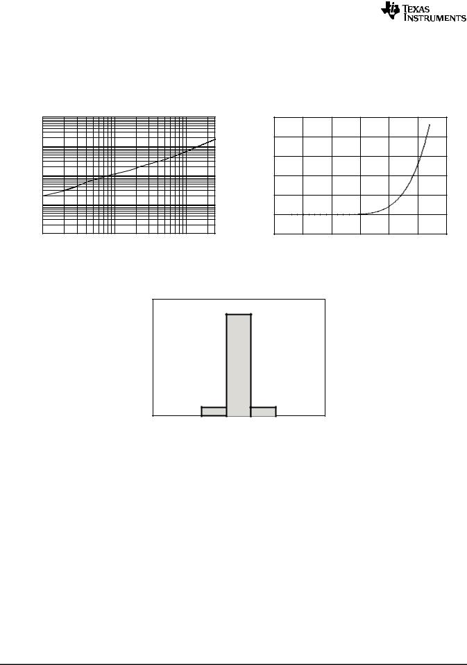
Figure 14. |
Figure 15. |
SupplyCurrent(mA)
|
|
SUPPLY CURRENT |
|
|
|
|
|
SUPPLY CURRENT |
|
|
|
|
|
|
vs |
|
|
|
|
|
vs |
|
|
|
|
TEMPERATURE |
|
|
|
|
|
SAMPLING RATE |
|
|
|
1.84 |
|
|
|
|
|
|
|
10 |
|
|
|
1.83 |
|
|
|
|
|
|
|
1 |
|
|
|
|
|
|
|
|
|
|
(mA) |
|
|
|
|
1.82 |
|
|
|
|
|
|
|
|
|
|
|
|
|
|
|
|
|
SupplyCurrent |
|
|
|
|
|
|
|
|
|
|
|
|
0.1 |
|
|
|
|
|
|
|
|
|
|
|
|
|
|
|
|
1.81 |
|
|
|
|
|
|
|
|
|
|
|
1.80 |
|
|
|
|
|
|
|
0.01 |
|
|
|
|
|
|
|
|
|
|
|
|
|
|
|
1.79 |
|
|
|
|
|
|
|
0.001 |
|
|
|
−50 |
−25 |
0 |
25 |
50 |
75 |
100 |
|
1 |
10 |
100 |
250 |
|
|
|
Temperature (°C) |
|
|
|
|
Sampling Rate (kHz) |
|
|
|
|
|
Figure 16. |
|
|
|
|
|
Figure 17. |
|
|
|
Copyright © 2007–2009, Texas Instruments Incorporated |
Submit Documentation Feedback |
13 |
Product Folder Link(s): ADS8326
ADS8326
SBAS343C –MAY 2007 –REVISED SEPTEMBER 2009 |
www.ti.com |
TYPICAL CHARACTERISTICS: VDD = +5V (continued)
At TA = +25°C, VDD = +5V, VREF = +5V. fSAMPLE = 250kHz, fCLK = 24 × fSAMPLE, unless otherwise noted.
ReferenceCurrent( A)
REFERENCE CURRENT |
POWER-DOWN CURRENT |
vs |
vs |
SAMPLING RATE |
TEMPERATURE |
1000 |
|
|
|
|
30 |
|
|
|
|
|
|
|
|
|
|
(nA) |
28 |
|
|
|
|
|
|
100 |
|
|
|
|
|
|
|
|
|
|
|
|
|
|
DownCurrent |
|
|
|
|
|
|
|
|
|
|
|
|
26 |
|
|
|
|
|
|
|
|
|
|
|
|
|
|
|
|
|
|
|
10 |
|
|
|
|
24 |
|
|
|
|
|
|
|
|
|
|
Power- |
22 |
|
|
|
|
|
|
1 |
|
|
|
|
|
|
|
|
|
|
|
|
|
|
|
|
|
|
|
|
|
|
|
|
|
|
|
|
20 |
|
|
|
|
|
|
0.1 |
|
|
|
|
18 |
|
|
|
|
|
|
1 |
10 |
100 |
250 |
|
−50 |
−25 |
0 |
25 |
50 |
75 |
100 |
|
Sampling Rate (kHz) |
|
|
|
|
|
|
Temperature (°C) |
|
|
|
Figure 18. |
Figure 19. |
OUTPUT CODE HISTOGRAM FOR A DC INPUT
(8192 Conversions)
|
|
|
6990 |
|
|
|
OCCURRENCE |
|
|
|
|
|
|
|
|
592 |
|
610 |
|
|
0 |
0 |
|
|
|
0 |
0 |
7FFC |
7FFD |
7FFE |
7FFF |
8000 |
8001 |
8002 |
CODE
Figure 20.
14 |
Submit Documentation Feedback |
Copyright © 2007–2009, Texas Instruments Incorporated |
Product Folder Link(s): ADS8326