


ADS8326
www.ti.com |
SBAS343C –MAY 2007–REVISED SEPTEMBER 2009 |
THEORY OF OPERATION
The ADS8326 is a classic Successive Approximation Register (SAR) Analog-to-Digital (A/D) converter. The architecture is based on capacitive redistribution that inherently includes a sample-and-hold function. The converter is fabricated on a 0.6μ CMOS process. The architecture and process allow the ADS8326 to acquire and convert an analog signal at up to 250,000 conversions per second while consuming less than 10mW from VDD.
Differential linearity for the ADS8326 is factory-adjusted via a package-level trim procedure. The state of the trim elements is stored in non-volatile memory and is continuously updated after each acquisition cycle, just prior to the start of the successive approximation operation. This process ensures that one complete conversion cycle always returns the part to its factory-adjusted state in the event of a power interruption.
The ADS8326 requires an external reference, an external clock, and a single power source (VDD). The external reference can be any voltage between 0.1V and VDD. The value of the reference voltage directly sets the range of the analog input. The reference input current depends on the conversion rate of the ADS8326.
The external clock can vary between 24kHz (1kHz throughput) and 6.0MHz (250kHz throughput). The duty cycle of the clock is essentially unimportant, as long as the minimum high and low times are at least 200ns (VDD = 4.75V or greater). The minimum clock frequency is set by the leakage on the internal capacitors to the ADS8326.
The analog input is provided to two input pins: +IN and –IN. When a conversion is initiated, the differential input on these pins is sampled on the internal capacitor array. While a conversion is in progress, both inputs are disconnected from any internal function.
The digital result of the conversion is clocked out by the DCLOCK input and is provided serially (most significant bit first) on the DOUT pin.
The digital data that is provided on the DOUT pin is for the conversion currently in progress–there is no
pipeline delay. It is possible to continue to clock the ADS8326 after the conversion is complete and to obtain the serial data least significant bit first. See the Timing Information section for more information.
Copyright © 2007–2009, Texas Instruments Incorporated |
Submit Documentation Feedback |
19 |
Product Folder Link(s): ADS8326
ADS8326
SBAS343C –MAY 2007 –REVISED SEPTEMBER 2009 |
www.ti.com |
ANALOG INPUT
The analog input of ADS8326 is differential. The +IN and –IN input pins allow for a differential input signal. The amplitude of the input is the difference between the +IN and –IN input, or (+IN) – (–IN). Unlike some converters of this type, the –IN input is not resampled later in the conversion cycle. When the converter goes into Hold mode or conversion, the voltage difference between +IN and –IN is captured on the internal capacitor array.
The range of the –IN input is limited to –0.3V to +0.5V. As a result of this limitation, the differential input could be used to reject signals that are common to both inputs in the specified range. Thus, the –IN input is best used to sense a remote signal ground that may move slightly with respect to the local ground potential.
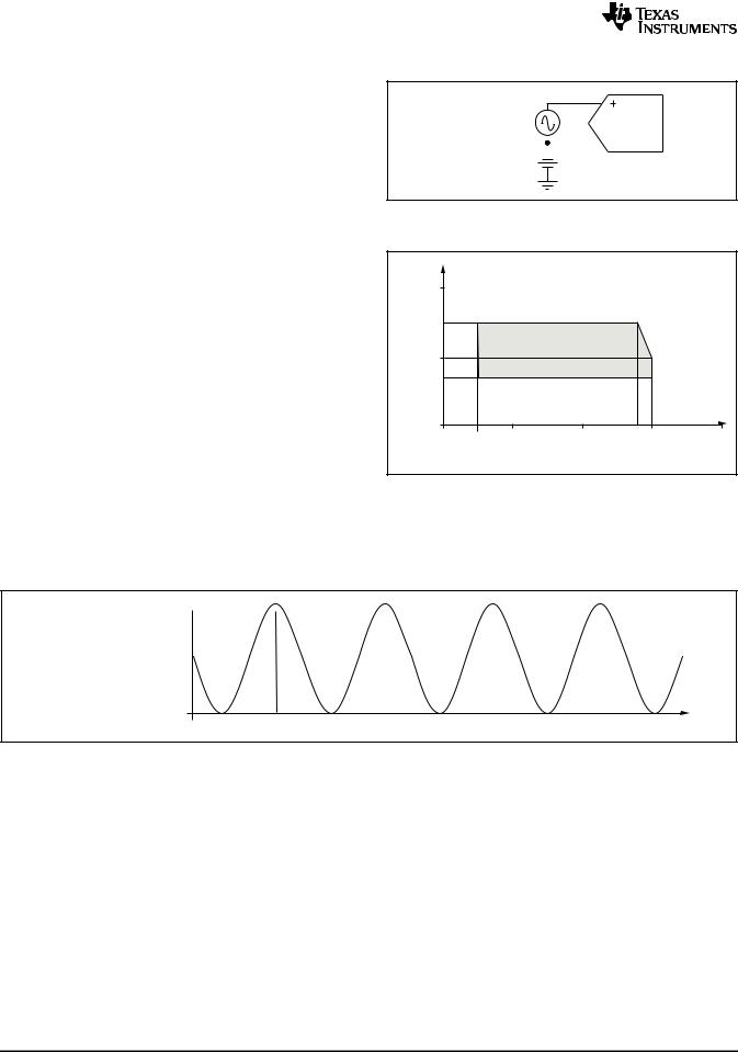
The general method for driving the analog input of the ADS8326 is shown in Figure 38 and Figure 40. The –IN input is held at the common-mode voltage. The +IN input swings from –IN (or common-mode voltage)
to –IN + VREF (or common-mode voltage + VREF ), and the peak-to-peak amplitude is +VREF . The value of VREF determines the range over which the
common-mode voltage may vary, as shown in Figure 39. Figure 6 and Figure 7 (+5V), and Figure 25 and Figure 26 (+2.7V) illustrate the typical change in gain and offset as a function of the common-mode voltage applied to the –IN pin.
0V to +VREF |
|
|
ADS8326 |
|||
Peak-to-Peak |
|
|
||||
|
|
|
|
|
||
|
|
|
|
|
|
|
|
|
|
|
|
|
|
Common-Mode
Voltage
Figure 38. Methods of Driving the ADS8326
(V) |
1 |
|
|
|
|
|
|
|
|
|
|
|
|
VDD = 5V |
|
Range |
0.5 |
|
|
|
|
|
|
|
|
|
|
|
|
|
|
CommonVoltage |
0 |
|
|
|
|
|
|
−0.3 |
|
|
|
|
|
|
|
|
|
|
|
|
|
|
|
|
−1 |
|
|
|
|
|
|
|
2 |
2.5 |
3 |
4 |
4.8 |
5 |
6 |
|
|
|
|
VREF (V) |
|
|
|
Figure 39. +IN Analog Input: Common-Mode
Voltage Range vs VREF
Common-Mode Voltage + VREF 
 +IN
+IN
+VREF
Common-Mode Voltage |
t |
−IN = Common-Mode Voltage
NOTE: The maximum differential voltage between +IN and –IN of the ADS8326 is VREF. See Figure 39 for a further explanation of the common-mode voltage range for differential inputs.
Figure 40. Differential Input Mode of the ADS8326
20 |
Submit Documentation Feedback |
Copyright © 2007–2009, Texas Instruments Incorporated |
Product Folder Link(s): ADS8326
|
|
|
|
|
|
|
|
|
|
|
|
ADS8326 |
||
www.ti.com |
|
|
|
|
|
|
|
|
SBAS343C –MAY 2007–REVISED SEPTEMBER 2009 |
|||||
The |
input current |
required by the analog |
inputs |
Single-Ended |
|
|
||||||||
depends on a number of factors: sample rate, input |
|
|
||||||||||||
|
|
|
|
|||||||||||
voltage, source impedance, and power-down mode. |
|
|
|
48PF |
||||||||||
Essentially, the current into the ADS8326 charges the |
10Ω |
+IN |
50Ω |
|||||||||||
|
||||||||||||||
|
|
|
|
|
|
|
|
|
|
|
|
|||
internal capacitor array during the sample |
period. |
OPA365 |
|
|
|
|||||||||
|
1000PF |
|
|
|||||||||||
After this capacitance has been fully charged, there is |
|
|
|
|||||||||||
|
|
ADS8326 |
|
|||||||||||
no further input current. The |
source of the |
analog |
|
|
|
|||||||||
|
|
|
|
|||||||||||
input |
voltage |
must |
be able |
to |
charge |
the |
input |
|
−IN |
50Ω |
48PF |
|||
|
|
|||||||||||||
capacitance (48pF) to a 16-bit settling level within 4.5 |
|
|
|
|||||||||||
|
|
|
|
|||||||||||
clock cycles (0.750μs). When the converter goes into |
|
|
|
|
||||||||||
Hold mode, or while it is in Power-Down mode, the |
|
|
|
|
||||||||||
input impedance is greater than 1GΩ. |
|
|
|
|
Differential |
|
|
|||||||
Care must be taken regarding the absolute analog |
|
|
|
|
||||||||||
input |
voltage. |
To |
maintain |
the |
linearity |
of |
the |
10Ω |
+IN |
50Ω |
48PF |
|||
converter, the –IN input should not drop below GND – |
|
|||||||||||||
|
|
|
||||||||||||
OPA365 |
|
|
|
|||||||||||
0.3V or exceed GND + 0.5V. The +IN input should |
|
1000PF |
|
|
||||||||||
always remain within the range of GND – 0.3V to VDD |
|
|
|
|
||||||||||
+ 0.3V, or –IN to –IN + VREF , whichever limit is |
|
1NF |
ADS8326 |
|
||||||||||
|
|
|
|
|||||||||||
reached first. Outside of these ranges, the converter |
10Ω |
|
50Ω |
48PF |
||||||||||
linearity may not meet |
specifications. To |
minimize |
−IN |
|
||||||||||
|
|
|
||||||||||||
OPA365 |
|
|
|
|||||||||||
noise, low bandwidth |
input |
signals with |
low-pass |
|
|
|
||||||||
|
1000PF |
|
|
|||||||||||
filters should be used. In each case, care should be |
|
|
|
|||||||||||
|
|
|
|
|||||||||||
taken to ensure that the output impedance of the |
|
|
|
|
||||||||||
sources driving the +IN and –IN inputs are matched. |
Figure 41. Single-Ended and Differential Methods |
|||||||||||||
Often, a small capacitor (20pF) between the positive |
||||||||||||||
of Interfacing the ADS8326 |
|
|||||||||||||
and negative inputs helps to match their impedance. |
|
|||||||||||||
|
|
|
|
|||||||||||
To obtain maximum performance from the ADS8326, |
|
|
|
|
||||||||||
the input circuit from Figure 41 is recommended. |
|
|
|
|
|
|||||||||
Copyright © 2007–2009, Texas Instruments Incorporated |
Submit Documentation Feedback |
21 |
Product Folder Link(s): ADS8326