


ADS8325
SBAS226C –MARCH 2002 –REVISED AUGUST 2007
LAYOUT
For optimum performance, care should be taken with the physical layout of the ADS8325 circuitry. This will be particularly true if the reference voltage is low and/or the conversion rate is high. At a 100kHz conversion rate, the ADS8325 makes a bit decision every 416ns. That is, for each subsequent bit decision, the digital output must be updated with the results of the last bit decision, the capacitor array appropriately switched and charged, and the input to the comparator settled to a 16-bit level all within one clock cycle.6
The basic SAR architecture is sensitive to spikes on the power supply, reference, and ground connections that occur just prior to latching the comparator output. Thus, during any single conversion for an n-bit SAR converter, there are n windows in which large external transient voltages can easily affect the conversion result. Such spikes might originate from switching power supplies, digital logic, and high-power devices, to name a few. This particular source of error can be very difficult to track down if the glitch is almost synchronous to the converter's DCLOCK signal as the phase difference between the two changes with time and temperature, causing sporadic misoperation.
With this in mind, power to the ADS8325 should be clean and well-bypassed. A 0.1μF ceramic bypass capacitor should be placed as close as possible to the ADS8325 package. In addition, a 1μF to 10μF capacitor and a 5Ω or 10Ω series resistor may be used to low-pass filter a noisy supply.
The reference should be similarly bypassed with a 47μF capacitor. Again, a series resistor and large capacitor can be used to low-pass filter the reference voltage. If the reference voltage originates from an op amp, make sure that the op amp can drive the bypass capacitor without oscillation (the series
www.ti.com
resistor can help in this case). Keep in mind that while the ADS8325 draws very little current from the reference on average, there are still instantaneous current demands placed on the external input and reference circuitry.
Texas Instruments' OPA627 op amp provides optimum performance for buffering both the signal and reference inputs. For low-cost, low-voltage, single-supply applications, the OPA2350 or OPA2340 dual op amps are recommended.
Also, keep in mind that the ADS8325 offers no inherent rejection of noise or voltage variation in regards to the reference input. This is of particular concern when the reference input is tied to the power supply. Any noise and ripple from the supply will appear directly in the digital results. While high-frequency noise can be filtered out as described in the previous paragraph, voltage variation due to the line frequency (50Hz or 60Hz) can be difficult to remove.
The GND pin on the ADS8325 should be placed on a clean ground point. In many cases, this will be the analog ground. Avoid connecting the GND pin too close to the grounding point for a microprocessor, microcontroller, or digital signal processor. If needed, run a ground trace directly from the converter to the power-supply connection point. The ideal layout will include an analog ground plane for the converter and associated analog circuitry.
22 |
Submit Documentation Feedback |
Copyright © 2002–2007, Texas Instruments Incorporated |
Product Folder Link(s): ADS8325

ADS8325
www.ti.com
SBAS226C –MARCH 2002 –REVISED AUGUST 2007
APPLICATION CIRCUITS
Figure 39 shows a basic data acquisition system. The ADS8325 input range is connected to 2.5V or 4.096V. The 5Ω resistor and 1μF to 10μF capacitor filters the microcontroller noise on the supply, as well as any
high-frequency noise from the supply itself. The exact values should be picked such that the filter provides adequate rejection of noise. Operational amplifiers and voltage reference are connected to analog power supply, AVDD.
DVDD 2.7V to 3.6V
+
0.1µF  10µF
10µF
AVDD |
|
|
|
|
5Ω |
|
2.7V to 5V |
|
|
|
|
|
|
|
REF5025 |
|
|
|
|
|
IN |
OUT |
|
REF |
VDD |
|
|
|
|
|
|
|
+ |
|
0.47µF |
GND |
4.7µF |
|
|
0.1µF |
10µF |
|
|
|
|
|
|
|
|
|
|
|
ADS8325 |
|
|
|
|
|
|
|
|
DSP |
|
|
50Ω |
|
|
|
TMS320C6xx |
|
|
OPA365 |
+IN |
|
|
or |
VCM + (0V to 2.5V) |
|
|
|
|
TMS320C5xx |
|
100pF |
|
|
|
|
||
|
|
|
|
CS |
or |
|
|
|
|
|
|
|
|
|
|
|
1nF |
|
|
TMS320C2xx |
|
|
|
|
DOUT |
|
|
|
|
|
|
|
|
|
|
|
50Ω |
|
|
DCLOCK |
|
|
|
|
|
|
|
|
|
|
OPA365 |
−IN |
|
GND |
GND |
|
VCM |
100pF |
|
|
|
|
|
|
|
|
|
|
|
|
|
|
|
|
|
DVDD |
|
|
|
|
|
|
4.5V to 5.5V |
+
0.1µF  10µF
10µF
AVDD |
5Ω |
4.3V to 5.5V |
|
REF5040 |
|
|
|
IN |
OUT |
REF |
VDD |
|
|
|
|
+ |
|
0.47µF |
GND |
4.7µF |
0.1µF |
10µF |
|
|
|||
|
|
|
ADS8325 |
|
|
50Ω |
|
|
Microcontroller |
|
OPA365 |
+IN |
|
or |
|
0V to 4.096V |
|
|
DSP |
|
|
100pF |
CS |
|
|
|
|
|
|
|
|
|
DOUT |
|
|
|
|
DCLOCK |
|
|
|
−IN |
GND |
GND |
Figure 39. Two Examples of a Basic Data Acquisition System
Copyright © 2002–2007, Texas Instruments Incorporated |
Submit Documentation Feedback |
23 |
Product Folder Link(s): ADS8325

ADS8325 |
|
|
|
|
www.ti.com |
SBAS226C –MARCH 2002 –REVISED AUGUST 2007 |
|
|
|
Revision History |
|
Changes from Revision B (June 2007) to Revision C |
Page |
|
∙ Changed note for DRB package............................................................................................................................................ |
7 |
|
∙ Changed second timing diagram from the top; moved Hi-Z to span the entire range of tSMPL ............................................. |
8 |
|
Changes from Revision A (June 2003) to Revision B |
Page |
|
∙ Changed format of document to current standard look ......................................................................................................... |
1 |
|
∙ Changed RON and C(SAMPLE) values in Equivalent Input Circuit.............................................................................................. |
3 |
|
∙ Added missing value from Digital Inputs, Input Current, B Grade (typo)............................................................................... |
3 |
|
∙ Added missing values from Sampling Dynamics, B Grade (typo) ......................................................................................... |
5 |
|
∙ Changed DRB package pinout drawing to include thermal pad outline (not to scale) .......................................................... |
7 |
|
∙ Changed timing diagram (added new diagram to existing figures) ....................................................................................... |
8 |
|
∙ Added Peak-to-Peak Noise For a DC Input vs Reference Voltage plot ............................................................................. |
11 |
|
∙ Changed input capcitance from 20pF to 40pF (regarding the source of the analog input voltage) .................................... |
16 |
|
∙ |
Changed Figure 31 ............................................................................................................................................................. |
17 |
∙ Changed Figure 33 capacitor from 47F to 47μF (typo) ....................................................................................................... |
18 |
|
∙ Changed VFS from 7FFFH to FFFFH in Figure 36............................................................................................................... |
20 |
|
∙ |
Changed Figure 39 ............................................................................................................................................................. |
23 |
24 |
Submit Documentation Feedback |
Copyright © 2002–2007, Texas Instruments Incorporated |
Product Folder Link(s): ADS8325

PACKAGE OPTION ADDENDUM
www.ti.com |
6-Aug-2007 |
|
|
PACKAGING INFORMATION
Orderable Device |
Status (1) |
Package |
Package |
Pins Package Eco Plan (2) |
Lead/Ball Finish |
MSL Peak Temp (3) |
||
|
|
Type |
Drawing |
|
Qty |
|
|
|
ADS8325IBDGKR |
ACTIVE |
MSOP |
DGK |
8 |
2500 |
Green (RoHS & |
CU NIPDAU |
Level-2-260C-1 YEAR |
|
|
|
|
|
|
no Sb/Br) |
|
|
ADS8325IBDGKRG4 |
ACTIVE |
MSOP |
DGK |
8 |
2500 |
Green (RoHS & |
CU NIPDAU |
Level-2-260C-1 YEAR |
|
|
|
|
|
|
no Sb/Br) |
|
|
ADS8325IBDGKT |
ACTIVE |
MSOP |
DGK |
8 |
250 |
Green (RoHS & |
CU NIPDAU |
Level-2-260C-1 YEAR |
|
|
|
|
|
|
no Sb/Br) |
|
|
ADS8325IBDGKTG4 |
ACTIVE |
MSOP |
DGK |
8 |
250 |
Green (RoHS & |
CU NIPDAU |
Level-2-260C-1 YEAR |
|
|
|
|
|
|
no Sb/Br) |
|
|
ADS8325IBDRBR |
ACTIVE |
SON |
DRB |
8 |
2500 |
Green (RoHS & |
CU NIPDAU |
Level-2-260C-1 YEAR |
|
|
|
|
|
|
no Sb/Br) |
|
|
ADS8325IBDRBRG4 |
ACTIVE |
SON |
DRB |
8 |
2500 |
Green (RoHS & |
CU NIPDAU |
Level-2-260C-1 YEAR |
|
|
|
|
|
|
no Sb/Br) |
|
|
ADS8325IBDRBT |
ACTIVE |
SON |
DRB |
8 |
250 |
Green (RoHS & |
CU NIPDAU |
Level-2-260C-1 YEAR |
|
|
|
|
|
|
no Sb/Br) |
|
|
ADS8325IBDRBTG4 |
ACTIVE |
SON |
DRB |
8 |
250 |
Green (RoHS & |
CU NIPDAU |
Level-2-260C-1 YEAR |
|
|
|
|
|
|
no Sb/Br) |
|
|
ADS8325IDGKR |
ACTIVE |
MSOP |
DGK |
8 |
2500 |
Green (RoHS & |
CU NIPDAU |
Level-2-260C-1 YEAR |
|
|
|
|
|
|
no Sb/Br) |
|
|
ADS8325IDGKT |
ACTIVE |
MSOP |
DGK |
8 |
250 |
Green (RoHS & |
CU NIPDAU |
Level-2-260C-1 YEAR |
|
|
|
|
|
|
no Sb/Br) |
|
|
ADS8325IDGKTG4 |
ACTIVE |
MSOP |
DGK |
8 |
250 |
Green (RoHS & |
CU NIPDAU |
Level-2-260C-1 YEAR |
|
|
|
|
|
|
no Sb/Br) |
|
|
ADS8325IDRBR |
ACTIVE |
SON |
DRB |
8 |
2500 |
Green (RoHS & |
CU NIPDAU |
Level-2-260C-1 YEAR |
|
|
|
|
|
|
no Sb/Br) |
|
|
ADS8325IDRBRG4 |
ACTIVE |
SON |
DRB |
8 |
2500 |
Green (RoHS & |
CU NIPDAU |
Level-2-260C-1 YEAR |
|
|
|
|
|
|
no Sb/Br) |
|
|
ADS8325IDRBT |
ACTIVE |
SON |
DRB |
8 |
250 |
Green (RoHS & |
CU NIPDAU |
Level-2-260C-1 YEAR |
|
|
|
|
|
|
no Sb/Br) |
|
|
ADS8325IDRBTG4 |
ACTIVE |
SON |
DRB |
8 |
250 |
Green (RoHS & |
CU NIPDAU |
Level-2-260C-1 YEAR |
|
|
|
|
|
|
no Sb/Br) |
|
|
(1)The marketing status values are defined as follows: ACTIVE: Product device recommended for new designs.
LIFEBUY: TI has announced that the device will be discontinued, and a lifetime-buy period is in effect.
NRND: Not recommended for new designs. Device is in production to support existing customers, but TI does not recommend using this part in a new design.
PREVIEW: Device has been announced but is not in production. Samples may or may not be available. OBSOLETE: TI has discontinued the production of the device.
(2)Eco Plan - The planned eco-friendly classification: Pb-Free (RoHS), Pb-Free (RoHS Exempt), or Green (RoHS & no Sb/Br) - please check http://www.ti.com/productcontent for the latest availability information and additional product content details.
TBD: The Pb-Free/Green conversion plan has not been defined.
Pb-Free (RoHS): TI's terms "Lead-Free" or "Pb-Free" mean semiconductor products that are compatible with the current RoHS requirements for all 6 substances, including the requirement that lead not exceed 0.1% by weight in homogeneous materials. Where designed to be soldered at high temperatures, TI Pb-Free products are suitable for use in specified lead-free processes.
Pb-Free (RoHS Exempt): This component has a RoHS exemption for either 1) lead-based flip-chip solder bumps used between the die and package, or 2) lead-based die adhesive used between the die and leadframe. The component is otherwise considered Pb-Free (RoHS compatible) as defined above.
Green (RoHS & no Sb/Br): TI defines "Green" to mean Pb-Free (RoHS compatible), and free of Bromine (Br) and Antimony (Sb) based flame retardants (Br or Sb do not exceed 0.1% by weight in homogeneous material)
(3)MSL, Peak Temp. -- The Moisture Sensitivity Level rating according to the JEDEC industry standard classifications, and peak solder temperature.
Addendum-Page 1

PACKAGE OPTION ADDENDUM
www.ti.com |
6-Aug-2007 |
|
|
Important Information and Disclaimer:The information provided on this page represents TI's knowledge and belief as of the date that it is provided. TI bases its knowledge and belief on information provided by third parties, and makes no representation or warranty as to the accuracy of such information. Efforts are underway to better integrate information from third parties. TI has taken and continues to take reasonable steps to provide representative and accurate information but may not have conducted destructive testing or chemical analysis on incoming materials and chemicals. TI and TI suppliers consider certain information to be proprietary, and thus CAS numbers and other limited information may not be available for release.
In no event shall TI's liability arising out of such information exceed the total purchase price of the TI part(s) at issue in this document sold by TI to Customer on an annual basis.
Addendum-Page 2

PACKAGE MATERIALS INFORMATION
www.ti.com |
6-Aug-2007 |
|
|
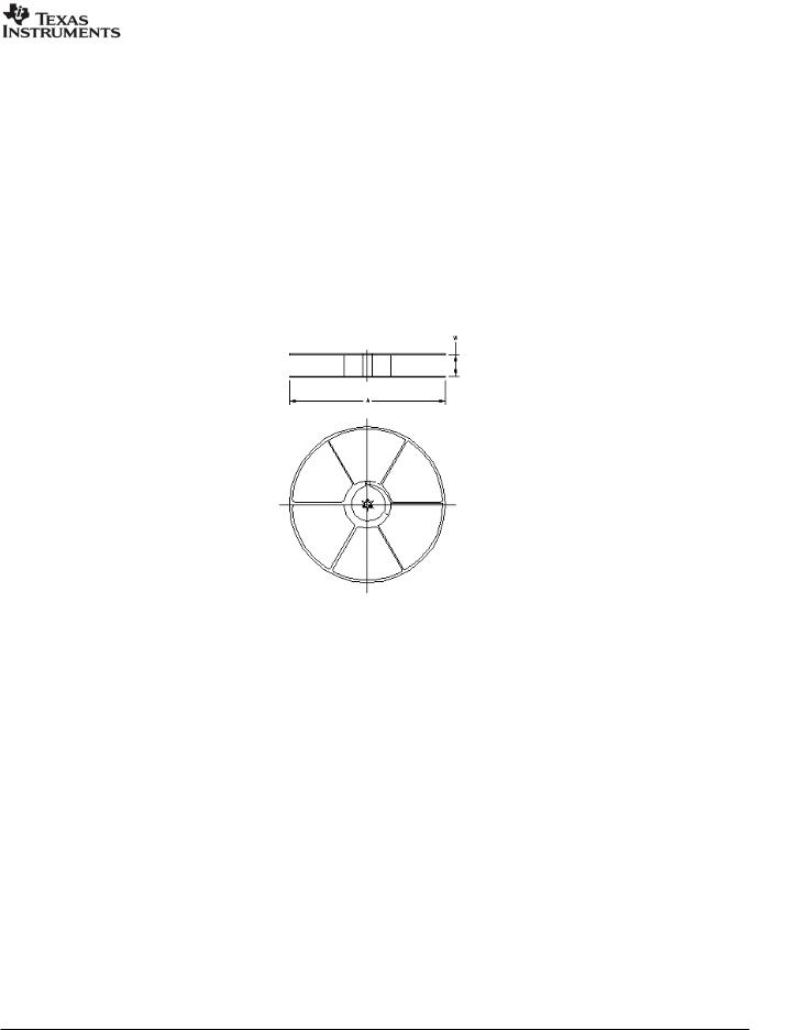
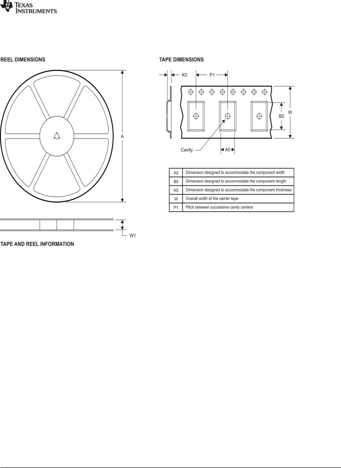
TAPE AND REEL INFORMATION
Pack Materials-Page 1
PACKAGE MATERIALS INFORMATION
www.ti.com |
|
|
|
|
|
|
|
|
|
|
6-Aug-2007 |
|
|
|
|
|
|
|
|
|
|
|
|
|
|
|
|
|
|
|
|
|
|
|
|
|
|
|
Device |
Package |
Pins |
Site |
Reel |
Reel |
A0 (mm) |
B0 (mm) |
K0 (mm) |
P1 |
W |
|
Pin1 |
|
|
|
|
Diameter |
Width |
|
|
|
(mm) |
(mm) |
|
Quadrant |
|
|
|
|
(mm) |
(mm) |
|
|
|
|
|
|
|
ADS8325IBDGKR |
DGK |
8 |
MLA |
330 |
12 |
5.2 |
3.3 |
1.6 |
12 |
12 |
|
NONE |
|
|
|
|
|
|
|
|
|
|
|
|
|
ADS8325IBDGKT |
DGK |
8 |
MLA |
330 |
12 |
5.2 |
3.3 |
1.6 |
12 |
12 |
|
NONE |
ADS8325IBDRBR |
DRB |
8 |
TUA |
330 |
12 |
3.3 |
3.3 |
1.1 |
8 |
12 |
|
Q2 |
|
|
|
|
|
|
|
|
|
|
|
|
|
ADS8325IBDRBT |
DRB |
8 |
TUA |
330 |
12 |
3.3 |
3.3 |
1.1 |
8 |
12 |
|
Q2 |
|
|
|
|
|
|
|
|
|
|
|
|
|
ADS8325IDGKR |
DGK |
8 |
MLA |
330 |
12 |
5.2 |
3.3 |
1.6 |
12 |
12 |
|
NONE |
ADS8325IDGKT |
DGK |
8 |
MLA |
330 |
12 |
5.2 |
3.3 |
1.6 |
12 |
12 |
|
NONE |
|
|
|
|
|
|
|
|
|
|
|
|
|
ADS8325IDRBR |
DRB |
8 |
TUA |
330 |
12 |
3.3 |
3.3 |
1.1 |
8 |
12 |
|
Q2 |
|
|
|
|
|
|
|
|
|
|
|
|
|
ADS8325IDRBT |
DRB |
8 |
TUA |
330 |
12 |
3.3 |
3.3 |
1.1 |
8 |
12 |
|
Q2 |
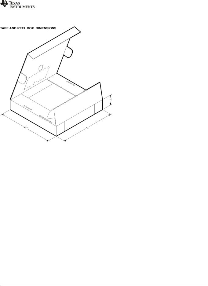
TAPE AND REEL BOX INFORMATION
Device |
Package |
Pins |
Site |
Length (mm) |
Width (mm) |
Height (mm) |
|
|
|
|
|
|
|
ADS8325IBDGKR |
DGK |
8 |
MLA |
390.0 |
348.0 |
63.0 |
|
|
|
|
|
|
|
ADS8325IBDGKT |
DGK |
8 |
MLA |
390.0 |
348.0 |
63.0 |
ADS8325IBDRBR |
DRB |
8 |
TUA |
0.0 |
0.0 |
0.0 |
|
|
|
|
|
|
|
ADS8325IBDRBT |
DRB |
8 |
TUA |
0.0 |
0.0 |
0.0 |
|
|
|
|
|
|
|
ADS8325IDGKR |
DGK |
8 |
MLA |
390.0 |
348.0 |
63.0 |
ADS8325IDGKT |
DGK |
8 |
MLA |
390.0 |
348.0 |
63.0 |
ADS8325IDRBR |
DRB |
8 |
TUA |
0.0 |
0.0 |
0.0 |
|
|
|
|
|
|
|
ADS8325IDRBT |
DRB |
8 |
TUA |
0.0 |
0.0 |
0.0 |
Pack Materials-Page 2

PACKAGE MATERIALS INFORMATION
www.ti.com |
6-Aug-2007 |
|
|
Pack Materials-Page 3

PACKAGE MATERIALS INFORMATION
www.ti.com |
16-Aug-2012 |
|
|
TAPE AND REEL INFORMATION
*All dimensions are nominal
Device |
Package |
Package |
Pins |
SPQ |
Reel |
Reel |
A0 |
B0 |
K0 |
P1 |
W |
Pin1 |
|
Type |
Drawing |
|
|
Diameter |
Width |
(mm) |
(mm) |
(mm) |
(mm) |
(mm) |
Quadrant |
|
|
|
|
|
(mm) |
W1 (mm) |
|
|
|
|
|
|
ADS8325IBDGKR |
VSSOP |
DGK |
8 |
2500 |
330.0 |
12.4 |
5.3 |
3.4 |
1.4 |
8.0 |
12.0 |
Q1 |
|
|
|
|
|
|
|
|
|
|
|
|
|
ADS8325IBDGKT |
VSSOP |
DGK |
8 |
250 |
180.0 |
12.4 |
5.3 |
3.4 |
1.4 |
8.0 |
12.0 |
Q1 |
|
|
|
|
|
|
|
|
|
|
|
|
|
ADS8325IBDRBR |
SON |
DRB |
8 |
2500 |
330.0 |
12.4 |
3.3 |
3.3 |
1.1 |
8.0 |
12.0 |
Q2 |
ADS8325IBDRBT |
SON |
DRB |
8 |
250 |
180.0 |
12.4 |
3.3 |
3.3 |
1.1 |
8.0 |
12.0 |
Q2 |
ADS8325IDGKR |
VSSOP |
DGK |
8 |
2500 |
330.0 |
12.4 |
5.3 |
3.4 |
1.4 |
8.0 |
12.0 |
Q1 |
|
|
|
|
|
|
|
|
|
|
|
|
|
ADS8325IDGKT |
VSSOP |
DGK |
8 |
250 |
180.0 |
12.4 |
5.3 |
3.4 |
1.4 |
8.0 |
12.0 |
Q1 |
|
|
|
|
|
|
|
|
|
|
|
|
|
ADS8325IDRBR |
SON |
DRB |
8 |
2500 |
330.0 |
12.4 |
3.3 |
3.3 |
1.1 |
8.0 |
12.0 |
Q2 |
ADS8325IDRBT |
SON |
DRB |
8 |
250 |
180.0 |
12.4 |
3.3 |
3.3 |
1.1 |
8.0 |
12.0 |
Q2 |
|
|
|
|
|
|
|
|
|
|
|
|
|
Pack Materials-Page 1
PACKAGE MATERIALS INFORMATION
www.ti.com |
16-Aug-2012 |
|
|
*All dimensions are nominal
Device |
Package Type |
Package Drawing |
Pins |
SPQ |
Length (mm) |
Width (mm) |
Height (mm) |
|
|
|
|
|
|
|
|
ADS8325IBDGKR |
VSSOP |
DGK |
8 |
2500 |
367.0 |
367.0 |
35.0 |
ADS8325IBDGKT |
VSSOP |
DGK |
8 |
250 |
210.0 |
185.0 |
35.0 |
|
|
|
|
|
|
|
|
ADS8325IBDRBR |
SON |
DRB |
8 |
2500 |
367.0 |
367.0 |
35.0 |
|
|
|
|
|
|
|
|
ADS8325IBDRBT |
SON |
DRB |
8 |
250 |
210.0 |
185.0 |
35.0 |
ADS8325IDGKR |
VSSOP |
DGK |
8 |
2500 |
367.0 |
367.0 |
35.0 |
|
|
|
|
|
|
|
|
ADS8325IDGKT |
VSSOP |
DGK |
8 |
250 |
210.0 |
185.0 |
35.0 |
|
|
|
|
|
|
|
|
ADS8325IDRBR |
SON |
DRB |
8 |
2500 |
367.0 |
367.0 |
35.0 |
ADS8325IDRBT |
SON |
DRB |
8 |
250 |
210.0 |
185.0 |
35.0 |
|
|
|
|
|
|
|
|
Pack Materials-Page 2
IMPORTANT NOTICE
Texas Instruments Incorporated and its subsidiaries (TI) reserve the right to make corrections, enhancements, improvements and other changes to its semiconductor products and services per JESD46, latest issue, and to discontinue any product or service per JESD48, latest issue. Buyers should obtain the latest relevant information before placing orders and should verify that such information is current and complete. All semiconductor products (also referred to herein as “components”) are sold subject to TI’s terms and conditions of sale supplied at the time of order acknowledgment.
TI warrants performance of its components to the specifications applicable at the time of sale, in accordance with the warranty in TI’s terms and conditions of sale of semiconductor products. Testing and other quality control techniques are used to the extent TI deems necessary to support this warranty. Except where mandated by applicable law, testing of all parameters of each component is not necessarily performed.
TI assumes no liability for applications assistance or the design of Buyers’ products. Buyers are responsible for their products and applications using TI components. To minimize the risks associated with Buyers’ products and applications, Buyers should provide adequate design and operating safeguards.
TI does not warrant or represent that any license, either express or implied, is granted under any patent right, copyright, mask work right, or other intellectual property right relating to any combination, machine, or process in which TI components or services are used. Information published by TI regarding third-party products or services does not constitute a license to use such products or services or a warranty or endorsement thereof. Use of such information may require a license from a third party under the patents or other intellectual property of the third party, or a license from TI under the patents or other intellectual property of TI.
Reproduction of significant portions of TI information in TI data books or data sheets is permissible only if reproduction is without alteration and is accompanied by all associated warranties, conditions, limitations, and notices. TI is not responsible or liable for such altered documentation. Information of third parties may be subject to additional restrictions.
Resale of TI components or services with statements different from or beyond the parameters stated by TI for that component or service voids all express and any implied warranties for the associated TI component or service and is an unfair and deceptive business practice. TI is not responsible or liable for any such statements.
Buyer acknowledges and agrees that it is solely responsible for compliance with all legal, regulatory and safety-related requirements concerning its products, and any use of TI components in its applications, notwithstanding any applications-related information or support that may be provided by TI. Buyer represents and agrees that it has all the necessary expertise to create and implement safeguards which anticipate dangerous consequences of failures, monitor failures and their consequences, lessen the likelihood of failures that might cause harm and take appropriate remedial actions. Buyer will fully indemnify TI and its representatives against any damages arising out of the use of any TI components in safety-critical applications.
In some cases, TI components may be promoted specifically to facilitate safety-related applications. With such components, TI’s goal is to help enable customers to design and create their own end-product solutions that meet applicable functional safety standards and requirements. Nonetheless, such components are subject to these terms.
No TI components are authorized for use in FDA Class III (or similar life-critical medical equipment) unless authorized officers of the parties have executed a special agreement specifically governing such use.
Only those TI components which TI has specifically designated as military grade or “enhanced plastic” are designed and intended for use in military/aerospace applications or environments. Buyer acknowledges and agrees that any military or aerospace use of TI components which have not been so designated is solely at the Buyer's risk, and that Buyer is solely responsible for compliance with all legal and regulatory requirements in connection with such use.
TI has specifically designated certain components as meeting ISO/TS16949 requirements, mainly for automotive use. In any case of use of non-designated products, TI will not be responsible for any failure to meet ISO/TS16949.
Products |
|
Applications |
|
Audio |
www.ti.com/audio |
Automotive and Transportation |
www.ti.com/automotive |
Amplifiers |
amplifier.ti.com |
Communications and Telecom |
www.ti.com/communications |
Data Converters |
dataconverter.ti.com |
Computers and Peripherals |
www.ti.com/computers |
DLP® Products |
www.dlp.com |
Consumer Electronics |
www.ti.com/consumer-apps |
DSP |
dsp.ti.com |
Energy and Lighting |
www.ti.com/energy |
Clocks and Timers |
www.ti.com/clocks |
Industrial |
www.ti.com/industrial |
Interface |
interface.ti.com |
Medical |
www.ti.com/medical |
Logic |
logic.ti.com |
Security |
www.ti.com/security |
Power Mgmt |
power.ti.com |
Space, Avionics and Defense |
www.ti.com/space-avionics-defense |
Microcontrollers |
microcontroller.ti.com |
Video and Imaging |
www.ti.com/video |
RFID |
www.ti-rfid.com |
|
|
OMAP Applications Processors |
www.ti.com/omap |
TI E2E Community |
e2e.ti.com |
Wireless Connectivity |
www.ti.com/wirelessconnectivity |
|
|
Mailing Address: Texas Instruments, Post Office Box 655303, Dallas, Texas 75265
Copyright © 2014, Texas Instruments Incorporated