

|
|
|
|
|
|
ADS8325 |
|
www.ti.com |
|
|
|
SBAS226C –MARCH 2002 –REVISED AUGUST 2007 |
|||
|
|
|
|
||||
50Ω |
+IN |
50Ω |
40pF |
50Ω |
+IN |
50Ω |
40pF |
|
|
|
|
||||
OPA365 |
|
|
OPA365 |
|
|
||
|
|
|
|
|
|
||
|
100pF |
|
|
100pF |
|
|
|
|
|
|
|
|
|
|
|
|
|
ADS8325 |
|
1nF |
|
ADS8325 |
|
|
−IN |
50Ω |
40pF |
50Ω |
−IN |
50Ω |
40pF |
|
|
|
|
|
|||
|
|
|
|
|
|
||
|
|
|
|
OPA365 |
|
|
|
|
|
|
|
100pF |
|
|
|
|
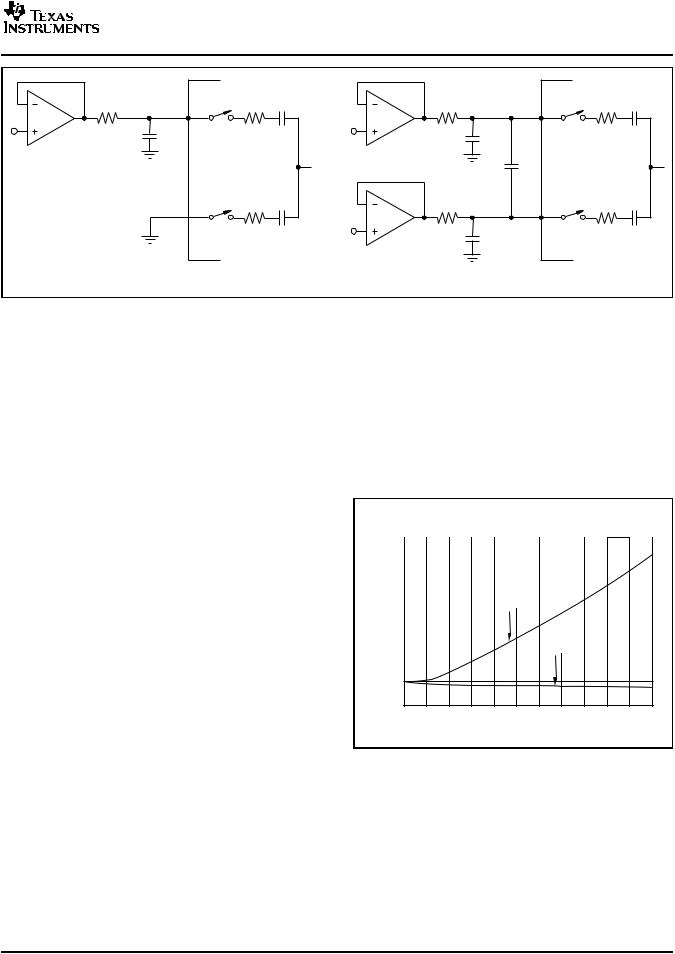
Single-Ended |
|
|
Differential |
|
|
|
Figure 31. Single-Ended and Differential Methods of Interfacing the ADS8325
REFERENCE INPUT
The external reference sets the analog input range. The ADS8325 will operate with a reference in the range of 2.5V to VDD. There are several important implications to this.
As the reference voltage is reduced, the analog voltage weight of each digital output code is reduced. This is often referred to as the Least Significant Bit (LSB) size and is equal to the reference voltage divided by 65,536. This means that any offset or gain error inherent in the A/D converter will appear to increase, in terms of LSB size, as the reference voltage is reduced. For a reference voltage of 2.5V, the value of LSB is 38.15μV, and for reference voltage of 5V, the LSB is 76.3μV.
The noise inherent in the converter will also appear to increase with lower LSB size. With a 5V reference, the internal noise of the converter typically contributes only 1.5LSBs peak-to-peak of potential error to the output code. When the external reference is 2.5V, the potential error contribution from the internal noise will be 2 times larger (3LSBs). The errors due to the internal noise are Gaussian in nature and can be reduced by averaging consecutive conversion results.
For more information regarding noise, consult Figure 9, Peak-to-Peak Noise vs Reference Voltage. Note that Figure 10, Effective Number Of Bits vs Input Frequency, is calculated based on the converter’s signal-to-(noise + distortion) ratio with a 1kHz, 0dB input signal. SINAD is related to ENOB as follows:
SINAD = 6.02 × ENOB + 1.76
As the difference between the power-supply voltage and reference voltage increases, the gain and offset performance of the converter will decrease. Figure 32 shows the typical change in gain and offset as a function of the difference between the power-supply voltage and reference voltage. For the combination of
VDD = 2.7V and VREF = 2.5V, or VDD = 5V and VREF = 5V, offset and gain error will be minimal. The most
dramatic difference in offset can be seen when VDD = 5V and VREF = 2.5V.
CHANGE IN OFFSET AND GAIN vs
SUPPLY/REFERENCE DIFFERENTIAL
|
3.0 |
|
|
|
|
|
|
|
|
2.5 |
|
|
|
|
|
|
|
|
|
|
|
|
|
|
|
|
Delta(mV) |
2.0 |
|
|
|
|
|
|
|
|
|
|
|
|
|
|
||
|
|
|
|
|
|
|
|
|
1.5 |
|
Offset |
|
|
|
|
||
|
|
|
|
|
|
|
||
|
|
|
|
|
|
|
|
|
|
|
|
|
|
|
|
|
|
|
1.0 |
|
|
|
|
|
|
|
|
|
|
|
|
|
|
|
|
|
|
|
|
|
|
Gain |
|
|
|
0.5 |
|
|
|
|
|
|
|
|
|
|
|
|
|
|
|
|
|
|
|
|
|
|
|
|
|
0
−0.5
00.25 0.50 0.75 1.00 1.25 1.50 1.75 2.00 2.25 2.50 2.75
VDD to VREF (V)
Figure 32. Change in Offset and Gain vs the Difference Between Power-Supply and Reference Voltage
Copyright © 2002–2007, Texas Instruments Incorporated |
Submit Documentation Feedback |
17 |
Product Folder Link(s): ADS8325
ADS8325
SBAS226C –MARCH 2002 –REVISED AUGUST 2007
With lower reference voltages, extra care should be taken to provide a clean layout including adequate bypassing, a clean power supply, a low-noise reference, and a low-noise input signal. Due to the lower LSB size, the converter will also be more sensitive to external sources of error, such as nearby digital signals and electromagnetic interference.
The equivalent input circuit for the reference voltage is presented in Figure 33. The 5kΩ resistor presents a constant load during the conversion process. At the same time, an equivalent capacitor of 20pF is switched. To obtain optimum performance from the ADS8325, special care must be taken in designing the interface circuit to the reference input pin. To ensure a stable reference voltage, a 47μF tantalum capacitor with low ESR should be connected as close as possible to the input pin. If a high output impedance reference source is used, an additional operational amplifier with a current limiting resistor must be placed in front of the capacitors.
|
ADS8325 |
100Ω |
20pF |
VREF |
|
OPA340 |
|
47µF |
5kΩ |
Figure 33. Input Reference Circuit and its Interface
When the ADS8325 is in power-down mode, the input resistance of the reference pin will have a value of 5GΩ. Since the input capacitors must be recharged before the next conversion starts, an operational amplifier with good dynamic characteristics must be used to buffer the reference input.
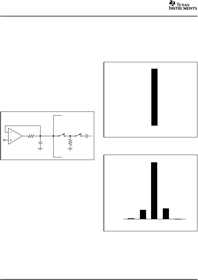
NOISE
The transition noise of the ADS8325 itself is extremely low (see Figure 34 and Figure 35); it is much lower than competing A/D converters. These histograms were generated by applying a low-noise DC input and initiating 5000 conversions. The digital output of the A/D converter will vary in output code due to the internal noise of the ADS8325. This is true for all 16-bit, SAR-type A/D converters. Using a histogram to plot the output codes, the distribution should appear bell-shaped with the peak of the bell curve representing the nominal code for the input value. The ±1σ, ±2σ, and ±3σ distributions will represent the 68.3%, 95.5%, and 99.7%, respectively, of all codes. The transition noise can be calculated by
www.ti.com
dividing the number of codes measured by 6 and this will yield the ±3σ distribution, or 99.7%, of all codes. Statistically, up to three codes could fall outside the distribution when executing 1000 conversions. The ADS8325, with < 3 output codes for the ±3σ distribution, will yield a < ±0.5LSBs of transition noise. Remember, to achieve this low-noise performance, the peak-to-peak noise of the input signal and reference must be < 50μV.
4005
VDD = 5.0V
VREF = 5.0V
519 |
|
476 |
|
||
0 |
|
|
|
|
0 |
|
|
|
|
|
|
7FFD 7FFE 7FFF |
8000 |
8001 |
|||
|
|
Code |
|
|
|
Figure 34. 5000 Conversion Histogram of a DC
Input
VDD = 2.7V |
|
3499 |
|
|
VREF = 2.5V |
|
|
|
|
|
649 |
|
683 |
|
|
|
|
|
|
90 |
|
|
|
79 |
7FFD |
7FFE |
7FFF |
8000 |
8001 |
|
|
Code |
|
|
Figure 35. 5000 Conversion Histogram of a DC
Input
18 |
Submit Documentation Feedback |
Copyright © 2002–2007, Texas Instruments Incorporated |
Product Folder Link(s): ADS8325