

Lab work performance.
Demonstrate presence of your home preparation for lab work to your instructor.
Pass test of 10 questions.
Get a permission to begin the work.
Mount the scheme of experiment 3A on the breadboard and perform it.
Make a conclusion about functionality of the scheme. Compare your results with theoretical ones.
Demonstrate your results to your instructor. If your results are correct you may dismount your scheme, if no – find the mistake.
Repeat steps 4 to 6 for experiment 3B, 3C, 3D.
Be ready to answer your instructor’s questions in process of work.
Complete your work, dismount your schemes, clean your working place.
Answer your instructor’s final questions, obtain your mark.
Ask your instructor’s permission to leave.
Experiment 3A.Realize the following circuit on a breadboard. Do not forget to connect 7thpin of 7404 chip to GND (0V) and 14thpin to VCC (+5V). Connecting X-input to either GND or VCC based on the following table, fill in the blanks. Write ON or OFF for LEDs.

-
INPUT
OUTPUT
X
LED1
LED2
1
0V
2
5V
As a result, this truth table belongs to a …………………………….
Experiment 3B.Realize the following circuit on a breadboard. Connecting X, and Y inputs to either GND or VCC based on the following table, fill in the blanks. Write ON or OFF for LEDs, and a voltage value for F.

|
|
|
|
INPUTS |
OUTPUTS | ||
|
|
X |
Y |
LED1 |
LED2 |
LED3 |
F (V) |
|
1 |
0V |
0V |
|
|
|
|
|
2 |
0V |
5V |
|
|
|
|
|
3 |
5V |
0V |
|
|
|
|
|
4 |
5V |
5V |
|
|
|
|
As a result this truth table belongs to a ……………………………………………….
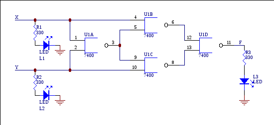
Experiment 3C.Realize the following circuit on a breadboard. Do not forget to connect 7thpin of 7400 chip to GND (0V) and 14thpin to VCC (+5V). Connecting X-input to either GND or VCC based on the following table, fill in the blanks. Write ON or OFF for LEDs.
|
|
|
|
INPUTS |
OUTPUTS | ||
|
|
X |
Y |
LED1 |
LED2 |
LED3 |
F (V) |
|
1 |
0V |
0V |
|
|
|
|
|
2 |
0V |
5V |
|
|
|
|
|
3 |
5V |
0V |
|
|
|
|
|
4 |
5V |
5V |
|
|
|
|
As a result this truth table belongs to a ………………………………….
Experiment 3D.Design XNOR gate on the same scheme basis. Draw the XNOR scheme with application of Scheme Design System.
|
|
|
|
INPUTS |
OUTPUTS | ||
|
|
X |
Y |
LED1 |
LED2 |
LED3 |
F (V) |
|
1 |
0V |
0V |
|
|
|
|
|
2 |
0V |
5V |
|
|
|
|
|
3 |
5V |
0V |
|
|
|
|
|
4 |
5V |
5V |
|
|
|
|
As a result this truth table belongs to a ………………………………….