

Test questions
1. A decoder is a combinatioal circuit that
A. converts binary information from n input lines to a maximum of 2nunique output lines
B. has 2n(or less) unique input lines and n output lines
C. selects binary information from one of many input lines and direct it to a single output line
D. receives information on a single line and transmits this information on one of 2npossible output lines
E. Converts binary information from n input lines to m output lines
2. Output of 1*4 demultiplexer is D1. What are selection lines?

A. 00 B. 01 C. 10 D. 11 E. any of them
3. What signals for XYZ inputs are applied if active output is D0?
A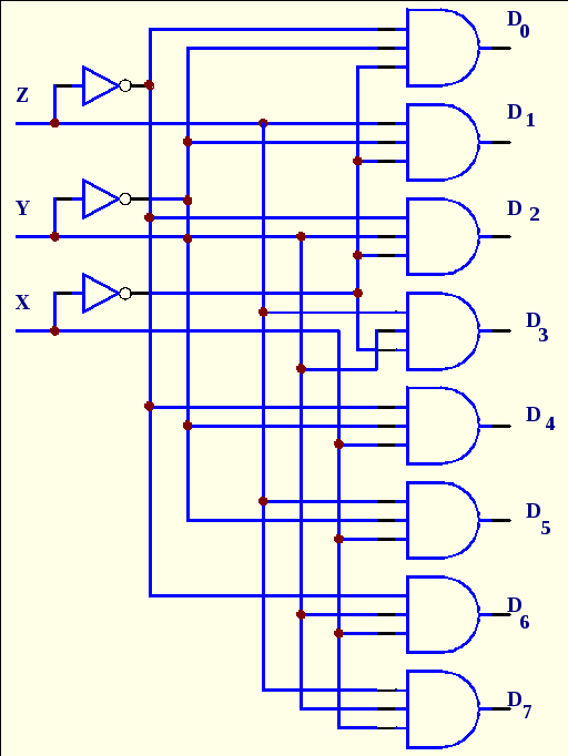 .0,
0, 0
.0,
0, 0
B. 0, 1, 1
C. 1, 0, 0
D. 0, 1, 0
E. 0, 0, 1
4. Decoder is __________ component.
A. SSI B. MSI C. LSI D. VLSI E. SSI or MSI
5. What function F1is implemented with a decoder and external gate?
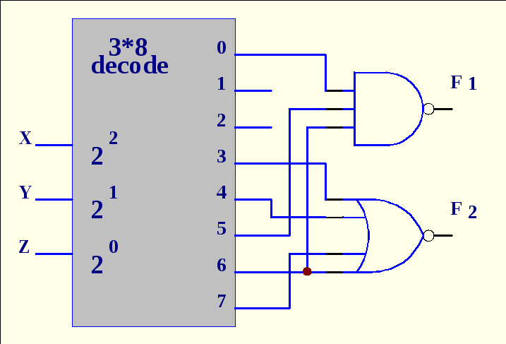
A. 0
B. 1
C. XY
D. X`Y`
E. XYZ`
6. What statement is correct?
A. A decoder can be realized on the basis of OR gates.
B. A decoder can be used as a MUX.
C. A decoder can be used as a data selector.
D. A 3-to-8 line decoder can be used for a binary-to-BCD conversion.
E. A 3-to-8 line decoder can be used for a binary-to-octal conversion.
7. What input signals must be applied to WXYZ for the circuit below if D8is generated as output?
A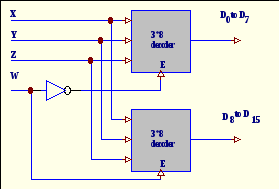 .
0110
.
0110
B. 0111
C. 1000
D. 1001
E. 1010
8. Fill in the gaps.
If we use NAND gates for decoder the outputs will be active-____. It means that only one output will be _______ at the moment, others will be _____.
A. HIGH, HIGH, LOW B. HIGH, LOW, HIGH C. LOW, HIGH, HIGH
D. LOW, LOW, HIGH E. all answers are wrong
9. DUX sometimes is called
A. code converter B. data selector C. data distributor
D. decoder E. all answers are correct
10. The scheme in question 3 is________.
A. 1-of-8 decoder B. 3-to-8 line decoder C. binary-to-octal decoder
D. A,B,C are correct E. A,B,C are wrong
Laboratory work # 9. Encoder.
Aims: investigate operation of the octal-to-binary encoder.
Preparation to lab work.
Learn the information about encoder
Consider the scheme of experiment 9A and define the results theoretically. Draw the scheme using Scheme Design System.
Implement the scheme of octal-to-binary encoder using OR gates and draw the scheme with application of Scheme Design System. This will be the scheme for the experiment 9B.
Answer the question below in written form.
What is an encoder?
What is a priority encoder?
Show the principal scheme of octal-to-binary and explain why D0is not connected with any of OR gates.
What discrepancy may be for this scheme? lab work performance.
Demonstrate presence of your home preparation for lab work to your instructor.
Pass test of 10 questions.
Get a permission to begin the work.
Mount the scheme of experiment 9A on the breadboard and perform it. Fill in the table.
Make a conclusion about functionality of the scheme. Compare your results with theoretical ones.
Demonstrate your results to your instructor. If your results are correct you may dismount your scheme, if no – find the mistake.
Repeat steps 4-6 for experiment 9B.
Be ready to answer your instructor’s questions in process of work.
Complete your work, dismount your schemes, clean your working place.
Answer your instructor’s final questions, obtain your mark.
Ask your instructor’s permission to leave.
Experiment 9A. Realize the following circuit on a breadboard. Connecting D0-D7to GND or VCC based on the following table, fill in the blanks. Write ON or OFF for LEDs. Remember that EI is active LOW enable input: a HIGH on this input forces all outputs to their inactive (HIGH) state; EO is active-LOW enable output: this output pin goes LOW when all inputs are inactive (HIGH) and EI is LOW; GS is active-LOW group signal output: this output pin goes LOW whenever any of the inputs are active (LOW) and EI is LOW.
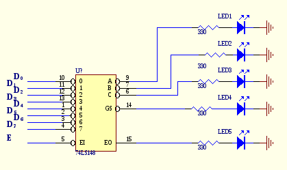
|
|
|
INPUTS |
OUTPUTS | ||||||||||||
|
|
|
(EI)’ |
D0’ |
D1’ |
D2’ |
D3’ |
D4’ |
D5’ |
D6’ |
D7’ |
GS’ |
A |
B |
C |
EO’ |
|
|
1 |
5 |
x |
x |
x |
x |
x |
x |
x |
x |
|
|
|
|
|
|
|
2 |
0 |
5 |
5 |
5 |
5 |
5 |
5 |
5 |
5 |
|
|
|
|
|
|
|
3 |
0 |
x |
x |
x |
x |
x |
x |
x |
0 |
|
|
|
|
|
|
|
4 |
0 |
x |
x |
x |
x |
x |
x |
0 |
5 |
|
|
|
|
|
|
|
5 |
0 |
x |
x |
x |
x |
x |
0 |
5 |
5 |
|
|
|
|
|
|
|
6 |
0 |
x |
x |
x |
x |
0 |
5 |
5 |
5 |
|
|
|
|
|
|
|
7 |
0 |
x |
x |
x |
0 |
5 |
5 |
5 |
5 |
|
|
|
|
|
|
|
8 |
0 |
x |
x |
0 |
5 |
5 |
5 |
5 |
5 |
|
|
|
|
|
|
|
9 |
0 |
x |
0 |
5 |
5 |
5 |
5 |
5 |
5 |
|
|
|
|
|
|
|
10 |
0 |
0 |
5 |
5 |
5 |
5 |
5 |
5 |
5 |
|
|
|
|
|
Experiment 9B. Implement the scheme of octal-to-binary encoder using OR gates and mount it on the breadboard. Fill in the table below. Compare your results with the table above.
|
|
|
INPUTS |
OUTPUTS | |||||||||
|
|
|
D0 |
D1 |
D2 |
D3 |
D4 |
D5 |
D6 |
D7 |
A |
B |
C |
|
|
1 |
5 |
0 |
0 |
0 |
0 |
0 |
0 |
0 |
|
|
|
|
|
2 |
0 |
5 |
0 |
0 |
0 |
0 |
0 |
0 |
|
|
|
|
|
3 |
5 |
5 |
0 |
0 |
0 |
0 |
0 |
0 |
|
|
|
|
|
4 |
0 |
0 |
5 |
0 |
0 |
0 |
0 |
0 |
|
|
|
|
|
5 |
0 |
5 |
5 |
0 |
0 |
0 |
0 |
0 |
|
|
|
|
|
6 |
0 |
0 |
5 |
0 |
0 |
5 |
0 |
0 |
|
|
|
|
|
7 |
0 |
0 |
0 |
5 |
0 |
0 |
0 |
0 |
|
|
|
|
|
8 |
0 |
0 |
0 |
0 |
5 |
0 |
0 |
0 |
|
|
|
|
|
9 |
0 |
0 |
5 |
5 |
5 |
5 |
5 |
5 |
|
|
|
|
|
10 |
0 |
5 |
5 |
5 |
5 |
5 |
5 |
5 |
|
|
|
Conclusion.