

Test questions
1. A multiplexer is a combinational circuit that
A.converts binary information from n input lines to a maximum of 2nunique output lines
B. has 2n(or less) unique input lines and n output lines
C. selects binary information from one of many input lines and direct it to a single output line
D. receives information on a single line and transmits this information on one of 2npossible output lines
E. converts binary information from n input lines to m output lines
2. Strobe is
A. Enable input of decoder b. Disable input of decoder
C. enable input of multiplexer D. disable input of demultiplexer
E. Disable input of multiplexer
3. What will the output signal of 4*1 multiplexer be if selection lines S1S0=11?

A. I0
B. I1
C. I2
D. I3
E. any of them
4. What are selection lines of 4*1 multiplexer if output signal Y=I1?
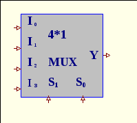
A. 00
B. 01
C. 10
D. 11
E. any of them
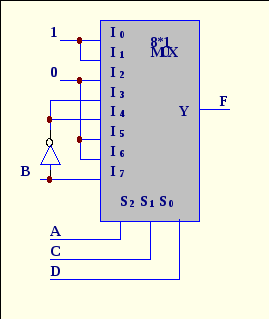
5. What function is implemented with multiplexer?
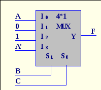
A. F(A,B,C)=Σ(2,3,5,6)
B. F(A,B,C)=Σ(1,3,5,6)
C. F(A,B,C)=Σ(2,3,5,7)
D.F(A,B,C)=Σ(2,3,4,6)
E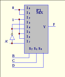 .
F(A,B,C)=Σ(1,3,5,7)
.
F(A,B,C)=Σ(1,3,5,7)
6. What function is implemented with multiplexer?
A. F(A,B,C,D)= Σ(2,5,6,7,10,11,12,13,14)
B. F(A,B,C,D)= Σ(0,1,3,4,7,14)
C. F(A,B,C,D)= Σ(0,1,3,4,8,15)
D. F(A,B,C,D)= Σ(0,1,3,4,8,9,15)
E. F(A,B,C,D)= Σ(0,1,3,5,7,14,15)
7. Decoder is __________ component.
A. SSI B. MSI C. LSI D. VLSI E. SSI or MSI
8. For the circuit below if selection lines S2S1S0=011 the output Z will be ____, if S2S1S0=100, Z will be ____, if S2S1S0=001, Z will be ____.

A. 1,1,0 B. 0,1,1 C. 1,1,1 D. 0,1,0 E.1,0,1
9. For the circuit in question 8 the output Z is equal to _____ for periods of time between t3and t4, t4and t5, t5and t6.
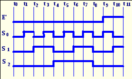
A. 0,1,1 B. 0,1,0 C. 1,1,1 D. 0,0,1 E. 1,0,1
10. What function is implemented with multiplexer?
A. F(A,B,C,D)= Σ(0,1,3,4,5,8,15)
B. F(A,B,C,D)= Σ(0,1,3,4,7,14)
C. F(A,B,C,D)= Σ(0,1,3,4,8,15)
D. F(A,B,C,D)= Σ(0,1,3,4,8,9,15)
E. F(A,B,C,D)= Σ(0,1,3,5,7,14,15)
Laboratory work # 11. D- flip-flop.
Aims: investigate operation of the D-flip-flop.
Preparation to lab work.
Learn the information about flip-flops.
Consider the scheme of experiment 11A and define the results theoretically. Draw the circuit with application of Scheme Design System.
Draw the D-flip-flop implemented with NAND gates (using Scheme Design System) for the experiment 11B.
Answer the question below in written form.
What circuit is called sequential?
What sequential circuit is called synchronous?
What sequential circuit is called asynchronous?
What is a master-clock generator?
What circuits are called clocked sequential circuits?
What is a flip-flop?
What types of flip-flops do you know?
Show truth tables for all types of flip-flops.
Show the typical schemes of RS, D, T, JK-flip-flops and describe their operation. (Use Scheme Design System).
What is a master-slave flip-flop?
What is setup time and hold time for flip-flop?
Show excitation tables for all types of flip-flops.
What types of flip-flops’ triggering do you know?