

Laboratory work # 2. Realization of logic gates with transistors.
Aims: define what logic gates are realized schematically, learn the gates’ properties. Compare experimental results with theoretical foundations about logic gates.
Improve skills of the schemes’ preparation.
Preparation to lab work.
Learn the information about transistors.
Show bipolar transistor’s characteristics.
Consider experiments’ schemes and draw them with application of Scheme Design System. Analyze what gates are realized on the schemes’ basis. Fill in the tables theoretically.
Answer the questions below in written form.
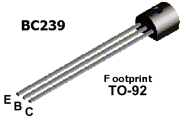
What is a bipolar transistor?
What are names of a bipolar transistor’s electrodes?
How to define situation of a bipolar transistor’s electrodes?
What are conditions to have a bipolar transistor ON(OFF)?
What types of bipolar transistors do you know?
What are typical silicon transistor’s parameters?
What modes of a bipolar transistor’s operation do you know?
Lab work performance.
Demonstrate presence of your home preparation for lab work to your instructor.
Pass test of 10 questions.
Get a permission to begin the work.
Mount the first scheme of experiment 2 on the breadboard and perform it.
Make a conclusion about functionality of the scheme. Compare your results with theoretical ones.
Demonstrate your results to your instructor. If your results are correct you may dismount your scheme, if no – find the mistake.
Repeat steps 4 to 6 for the second and third schemes of experiment 2.
Be ready to answer your instructor’s questions in process of work.
Complete your work, dismount your schemes, clean your working place.
Answer your instructor’s final questions, obtain your mark.
Ask your instructor’s permission to leave.
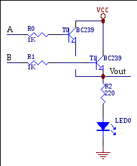
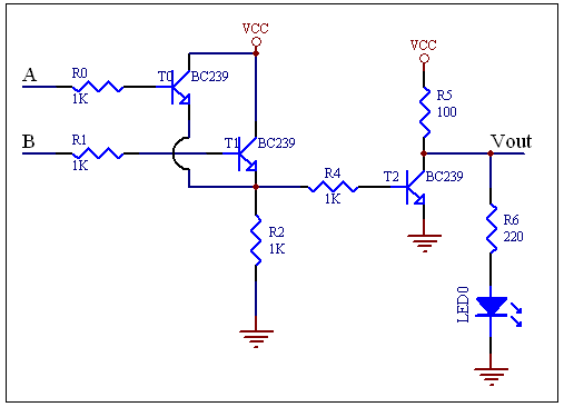
Experiment 2.Realize the following circuit on a breadboard. Connecting A, and B inputs to either GND or VCC based on the following table, fill in the blanks. Write ON or OFF for LEDs.
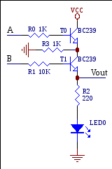

|
INPUTS OUTPUTS
A B LED Vout 1 0V 0V
2 0V 5V
3 5V 0V
4 5V 5V
| ||||||||||||||||||||||||||||||||||||||||||||||||||||||||||||
This is …………… Gate This is a ……………. Gate
|
INPUTS OUTPUTS
A B LED Vout 1 0V 0V
2 0V 5V
3 5V 0V
4 5V 5V
| ||||||||||||||||||||||||||||||||||||||||||||||||||||||||||||
This is …………… Gate This is a ……………. Gate