- •Suleyman demirel university
- •Contents
- •Preface
- •Preliminaries 1. Resistors’ colored codes.
- •Preliminaries 2. Measurements with digital multimeter.
- •Laboratory work # 1. Diode applications
- •Preparation to lab work.
- •Lab work performance.
- •Test questions
- •Laboratory work # 2. Realization of logic gates with transistors.
- •Preparation to lab work.
- •Lab work performance.
- •Test questions
- •A. On, on, on b. On, on, off c. Off,on, off
- •A. 1 p-n-junction b. 2 p-n-junctions c. 3 p-n-junctions
- •A. On, on, on b. On, on, off c. Off,on, off
- •A. On, on, on b. On, off, off c. Off,on, off
- •Laboratory work # 3. Logic gates.
- •Preparation to lab work.
- •Lab work performance.
- •Test questions
- •A. 1 b. 2 c. 3 d. 4 e. 5
- •A. Xor b. Xnor c. Nor d. Nand e. And
- •5. Nor is dual to a. Xor b. Xnor c. Nor d. Nand e. And
- •6. Or is complement to a. Xor b. Xnor c. Nor d. Nand e. And
- •A.1 b.2 c.3 d.4 e 5
- •Laboratory work # 4. Seven-segment displays
- •Preparation to lab work.
- •Lab work performance.
- •Test questions
- •A. Makes the several systems compatible b. Makes the two systems compatible c. Makes the two systems compatible even though each uses a different binary code
- •A. 0,0,1 b.1,0,1 c.1,1,0 d.0,1,0 e. 0,1,1
- •Laboratory work # 5. Four-bit binary parallel adder.
- •Preparation to lab work.
- •Lab work performance.
- •Test questions
- •A. Binary numbers b. Binary variables
- •A.Sequential; three
- •Test questions
- •A.Sequential; three b. Sequential; two c. Combinational; two d. Combinational; three e. Sequential or combinational; three
- •E. The sum of two bits and a previous carry, … the sum of two bits
- •Lab work performance.
- •Test questions
- •A. 1 b. 2 c. 3 d. 4 e. 5
- •A. Xor b. Xnor c. Nor d. Nand e. And
- •Laboratory work # 8. Decoder and demultiplexer.
- •Preparation to lab work.
- •Lab work performance.
- •Table #1
- •Table #2
- •Test questions
- •E. Converts binary information from n input lines to m output lines
- •Laboratory work # 9. Encoder.
- •Preparation to lab work.
- •What discrepancy may be for this scheme? lab work performance.
- •Test questions
- •Laboratory work # 10.
- •Test questions
- •A. Enable input of decoder b. Disable input of decoder
- •E. Disable input of multiplexer
- •Laboratory work # 11. D- flip-flop.
- •Preparation to lab work.
- •Lab work performance.
- •Test questions
- •A. Rs and clocked rs b.Rs or clocked rs c. D d. Jk e. T
- •A. Rs b. Clocked rs c. D d. Jk e. T
- •A. An expression to describe next state of the circuit
- •A. 1 b. 2 c. 3 d. 4 e. 5
- •Lab work performance.
- •Test questions
- •E. Decoder with enable can be used as multiplexer
- •A. 0000, 0001, 0010, 0011 b. 0000, 1000, 1100, 1110 c. 0000, 1000, 1001, 1010 d. 0000, 1000, 0001, 1001 e. 0000, 0001, 1000, 1001
- •A. 1, 0, 1
- •Test questions
- •A. A, c, d, e, f, g b. A, c, d, e, f c. A, b, c, f, g d. C, d, e, f, g e. A, b, c, d, e, f
- •A. To make a device active b. To provide the normal device’s operation
- •Laboratory work # 14. Bidirectional shift register.
- •Preparation to lab work.
- •Lab work performance.
- •Test questions
Preparation to lab work.
Learn the information about decoder and demultiplexer.
Consider the scheme of experiment 8A and define the results theoretically. Draw the scheme using Scheme Design System.
Construct 3*8 decoder using 2 decoder/demultiplexer ICs (74139) and an inverter for experiment 8B. Draw it using Scheme Design System.
Answer the question below in written form.
What is a decoder?
What is a DUX?
Show the principal scheme of 2*4 decoder with application of Scheme Design System.
What is enable input for a decoder?
Decoder with an enable input can work as ________.
Compare decoder and encoder.
Compare DUX and MUX.
Show the scheme of 2*4 decoder on the basis of NOR gates (use Scheme Design System).
Lab work performance.
Demonstrate presence of your home preparation for lab work to your instructor.
Pass test of 10 questions.
Get a permission to begin the work.
Mount the scheme of experiment 8A on the breadboard and perform it. Fill in table #1.
Make a conclusion about functionality of the scheme. Compare your results with theoretical ones.
Demonstrate your results to your instructor. If your results are correct you may dismount your scheme, if no – find the mistake.
Repeat steps 4-6 for the experiment 8B.
Demonstrate your results to your instructor. If your results are correct you may dismount your scheme, if no – find the mistake.
Be ready to answer your instructor’s questions in process of work.
Complete your work, dismount your schemes, clean your working place.
Answer your instructor’s final questions, obtain your mark.
Ask your instructor’s permission to leave.
Experiment 8A.Realize the circuit below on the breadboard.
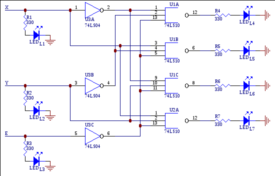
Table #1
|
INPUTS |
OUTPUTS | ||||||||
|
E |
X |
Y |
LED1 |
LED2 |
LED3 |
LED4 |
LED5 |
LED6 |
LED7 |
1 |
0V |
0V |
0V |
|
|
|
|
|
|
|
2 |
0V |
0V |
5V |
|
|
|
|
|
|
|
3 |
0V |
5V |
0V |
|
|
|
|
|
|
|
4 |
0V |
5V |
5V |
|
|
|
|
|
|
|
5 |
5V |
X |
X |
|
|
|
|
|
|
|
As a result, this truth table belongs to a …………………………….
Experiment 8B.Construct 3*8 decoder using 2 decoder/demultiplexer ICs (74139) and an inverter. Mount the scheme on a breadboard and fill the table below.
Table #2
|
INPUTS |
OUTPUTS | ||||||||||||
|
X |
Y |
Z |
L1 |
L2 |
L3 |
L4 |
L5 |
L6 |
L7 |
L8 |
L9 |
L10 |
L11 |
1 |
0V |
0V |
0V |
|
|
|
|
|
|
|
|
|
|
|
2 |
0V |
0V |
5V |
|
|
|
|
|
|
|
|
|
|
|
3 |
0V |
5V |
0V |
|
|
|
|
|
|
|
|
|
|
|
4 |
0V |
5V |
5V |
|
|
|
|
|
|
|
|
|
|
|
5 |
5V |
0V |
0V |
|
|
|
|
|
|
|
|
|
|
|
6 |
5V |
0V |
5V |
|
|
|
|
|
|
|
|
|
|
|
7 |
5V |
5V |
0V |
|
|
|
|
|
|
|
|
|
|
|
8 |
5V |
5V |
5V |
|
|
|
|
|
|
|
|
|
|
|