- •Suleyman demirel university
- •Contents
- •Preface
- •Preliminaries 1. Resistors’ colored codes.
- •Preliminaries 2. Measurements with digital multimeter.
- •Laboratory work # 1. Diode applications
- •Preparation to lab work.
- •Lab work performance.
- •Test questions
- •Laboratory work # 2. Realization of logic gates with transistors.
- •Preparation to lab work.
- •Lab work performance.
- •Test questions
- •A. On, on, on b. On, on, off c. Off,on, off
- •A. 1 p-n-junction b. 2 p-n-junctions c. 3 p-n-junctions
- •A. On, on, on b. On, on, off c. Off,on, off
- •A. On, on, on b. On, off, off c. Off,on, off
- •Laboratory work # 3. Logic gates.
- •Preparation to lab work.
- •Lab work performance.
- •Test questions
- •A. 1 b. 2 c. 3 d. 4 e. 5
- •A. Xor b. Xnor c. Nor d. Nand e. And
- •5. Nor is dual to a. Xor b. Xnor c. Nor d. Nand e. And
- •6. Or is complement to a. Xor b. Xnor c. Nor d. Nand e. And
- •A.1 b.2 c.3 d.4 e 5
- •Laboratory work # 4. Seven-segment displays
- •Preparation to lab work.
- •Lab work performance.
- •Test questions
- •A. Makes the several systems compatible b. Makes the two systems compatible c. Makes the two systems compatible even though each uses a different binary code
- •A. 0,0,1 b.1,0,1 c.1,1,0 d.0,1,0 e. 0,1,1
- •Laboratory work # 5. Four-bit binary parallel adder.
- •Preparation to lab work.
- •Lab work performance.
- •Test questions
- •A. Binary numbers b. Binary variables
- •A.Sequential; three
- •Test questions
- •A.Sequential; three b. Sequential; two c. Combinational; two d. Combinational; three e. Sequential or combinational; three
- •E. The sum of two bits and a previous carry, … the sum of two bits
- •Lab work performance.
- •Test questions
- •A. 1 b. 2 c. 3 d. 4 e. 5
- •A. Xor b. Xnor c. Nor d. Nand e. And
- •Laboratory work # 8. Decoder and demultiplexer.
- •Preparation to lab work.
- •Lab work performance.
- •Table #1
- •Table #2
- •Test questions
- •E. Converts binary information from n input lines to m output lines
- •Laboratory work # 9. Encoder.
- •Preparation to lab work.
- •What discrepancy may be for this scheme? lab work performance.
- •Test questions
- •Laboratory work # 10.
- •Test questions
- •A. Enable input of decoder b. Disable input of decoder
- •E. Disable input of multiplexer
- •Laboratory work # 11. D- flip-flop.
- •Preparation to lab work.
- •Lab work performance.
- •Test questions
- •A. Rs and clocked rs b.Rs or clocked rs c. D d. Jk e. T
- •A. Rs b. Clocked rs c. D d. Jk e. T
- •A. An expression to describe next state of the circuit
- •A. 1 b. 2 c. 3 d. 4 e. 5
- •Lab work performance.
- •Test questions
- •E. Decoder with enable can be used as multiplexer
- •A. 0000, 0001, 0010, 0011 b. 0000, 1000, 1100, 1110 c. 0000, 1000, 1001, 1010 d. 0000, 1000, 0001, 1001 e. 0000, 0001, 1000, 1001
- •A. 1, 0, 1
- •Test questions
- •A. A, c, d, e, f, g b. A, c, d, e, f c. A, b, c, f, g d. C, d, e, f, g e. A, b, c, d, e, f
- •A. To make a device active b. To provide the normal device’s operation
- •Laboratory work # 14. Bidirectional shift register.
- •Preparation to lab work.
- •Lab work performance.
- •Test questions
A.Sequential; three
B. sequential; two
C. combinational; two
D. combinational; three
E. sequential or combinational; three
9. Make addition of binary numbers: 1001 and 1010. Result is
A. 10011 B.1001 C. 1100 D. 11001 E. 10101
10. To construct 6-bit parallel adder we must use cascade of such full-adders IC s as
A. two 2-bit and one 1-bit B. one 2-bit and one 3-bit C.one 4-bit and one 1-bit
D. five 1-bit E. none of above mentioned, because 5-bit parallel adder IC exists itself
LABORATORY WORK # 6.
BCD ADDER.
Aims: investigate BCD adder operation, make an addition according to the task. Compare the results of the addition with ones, made by theoretical way.
PREPARATION TO LAB WORK.
Learn the information about BCD adder and combinational logic.
Draw block diagram of a BCD adder with application of Scheme Design System and compare this scheme with a scheme of experiment #6.
Answer the questions below in written form.
What is a decimal adder?
What is a BCD adder?
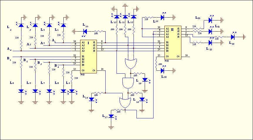
For what purpose do 3 external gates exist in the scheme of BCD adder?
LAB WORK PERFORMANCE.
Demonstrate presence of your home preparation for lab work to your instructor.
Pass test of 10 questions.
Get a permission to begin the work.
Mount the scheme of experiment 6 on the breadboard and perform it.
Make a conclusion about functionality of the scheme. Compare your results with theoretical ones.
Demonstrate your results to your instructor. If your results are correct you may dismount your scheme, if no – find the mistake.
Be ready to answer your instructor’s questions in process of work.
Complete your work, dismount your schemes, clean your working place.
Answer your instructor’s final questions, obtain your mark.
Ask your instructor’s permission to leave.
Experiment 6.Realize the circuit on a breadboard. For 2-input AND take 7408, pins 1,2-inputs, pin 3 output. For 2-input OR take 7432, pins 1,2,4,5-inputs, pins 3,6-outputs. Fill in the tables. Connect pin 5 of 7483 to VCC and pin 12 – to GND. Show ONs or OFFs for LEDs. Tasks for addition:
options |
Inputs of basic adder |
Outputs of basic adder | ||||||||||||
|
L1 |
L2 |
L3 |
L4 |
L5 |
L6 |
L7 |
L8 |
L9 |
L10 |
L11 |
L12 |
L13 |
L14 |
5+9 |
|
|
|
|
|
|
|
|
|
|
|
|
|
|
7+8 |
|
|
|
|
|
|
|
|
|
|
|
|
|
|
4+3 |
|
|
|
|
|
|
|
|
|
|
|
|
|
|
options |
Inputs of correction adder |
Outputs of the circuit | |||||||
|
L15 |
L16 |
L17 |
L18 |
L19 |
L20 |
L21 |
L22 |
L23 |
5+9 |
|
|
|
|
|
|
|
|
|
7+8 |
|
|
|
|
|
|
|
|
|
4+3 |
|
|
|
|
|
|
|
|
|
Conclusion: