

ADSP-BF531/ADSP-BF532/ADSP-BF533
General-Purpose I/O Port F Pin Cycle Timing
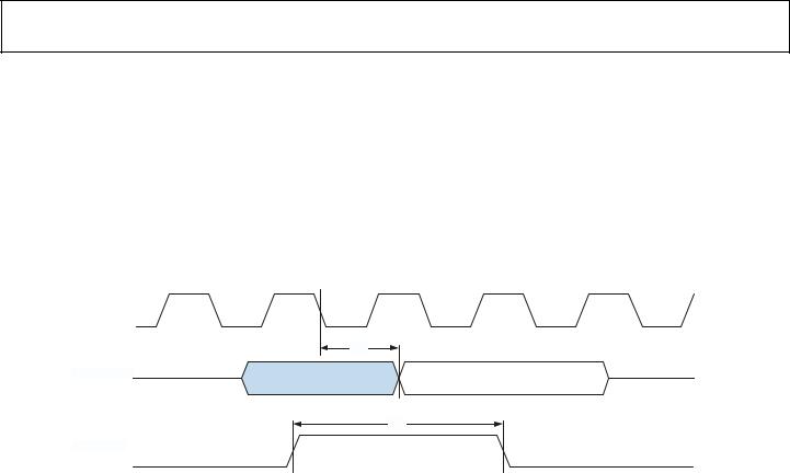
Table 28 and Figure 27 describe GPIO pin operations.
Table 28. General-Purpose I/O Port F Pin Cycle Timing
|
|
VDDEXT = 1.8 V |
VDDEXT = 2.5 V/3.3 V |
|
||
Parameter |
Min |
Max |
Min |
Max |
Unit |
|
Timing Requirement |
|
|
|
|
|
|
tWFI |
GPIO Input Pulse Width |
tSCLK + 1 |
|
tSCLK + 1 |
|
ns |
Switching Characteristic |
|
|
|
|
|
|
tDFO |
GPIO Output Delay from CLKOUT Low |
|
6 |
|
6 |
ns |
CLKOUT
tDFO
PFx (OUTPUT)
GPIO OUTPUT
tWFI
PFx (INPUT)
GPIO INPUT
Figure 27. GPIO Cycle Timing
Rev. E | Page 40 of 60 | July 2007
ADSP-BF531/ADSP-BF532/ADSP-BF533
Timer Cycle Timing
Table 29 and Figure 28 describe timer expired operations. The input signal is asynchronous in width capture mode and exter nal clock mode and has an absolute maximum input frequency of fSCLK/2 MHz.
Table 29. Timer Cycle Timing
|
|
|
VDDEXT = 1.8 V |
VDDEXT = 2.5 V/3.3 V |
|
|
Parameter |
Min |
Max |
Min |
Max |
Unit |
|
Timing Characteristics |
|
|
|
|
|
|
tWL |
Timer Pulse Width Input Low1 (Measured in SCLK Cycles) |
1 |
|
1 |
|
SCLK |
tWH |
Timer Pulse Width Input High1 (Measured in SCLK Cycles) |
1 |
|
1 |
|
SCLK |
Switching Characteristic |
|
|
|
|
|
|
tHTO |
Timer Pulse Width Output2 (Measured in SCLK Cycles) |
1 |
(232–1) |
1 |
(232–1) |
SCLK |
1 The minimum pulse widths apply for TMRx input pins in width capture and external clock modes. They also apply to the PF1 or PPI_CLK input pins in PWM output mode. 2 The minimum time for tHTO is one cycle, and the maximum time for tHTO equals (232–1) cycles.
CLKOUT
tHTO
TMRx
(PWM OUTPUT MODE)
TMRx |
|
tWL |
|
|
|
tWH |
|
|
|
|
|
(WIDTH CAPTURE AND EXTERNAL CLOCK MODES)
Figure 28. Timer PWM_OUT Cycle Timing
Rev. E | Page 41 of 60 | July 2007
ADSP-BF531/ADSP-BF532/ADSP-BF533
JTAG Test and Emulation Port Timing
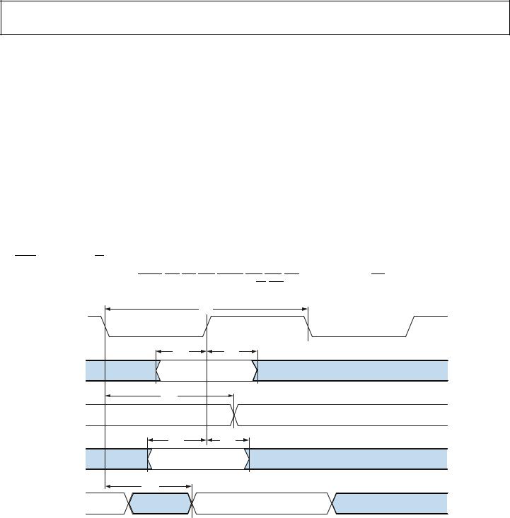
Table 30 and Figure 29 describe JTAG port operations.
Table 30. JTAG Port Timing
|
|
|
|
VDDEXT = 1.8 V |
VDDEXT = 2.5 V/3.3 V |
|
|
Parameter |
Min |
Max |
Min |
Max |
Unit |
||
Timing Requirements |
|
|
|
|
|
||
tTCK |
TCK Period |
20 |
|
20 |
|
ns |
|
tSTAP |
TDI, TMS Setup Before TCK High |
4 |
|
4 |
|
ns |
|
tHTAP |
TDI, TMS Hold After TCK High |
4 |
|
4 |
|
ns |
|
tSSYS |
System Inputs Setup Before TCK High1 |
4 |
|
4 |
|
ns |
|
tHSYS |
System Inputs Hold After TCK High1 |
5 |
|
5 |
|
ns |
|
tTRSTW |
|
Pulse Width2 (Measured in TCK Cycles) |
4 |
|
4 |
|
TCK |
TRST |
|
|
|||||
Switching Characteristics |
|
|
|
|
|
||
tDTDO |
TDO Delay from TCK Low |
|
10 |
|
10 |
ns |
|
tDSYS |
System Outputs Delay After TCK Low3 |
0 |
12 |
0 |
12 |
ns |
|
1System Inputs = DATA15–0, ARDY, TMR2–0, PF15–0, PPI_CLK, RSCLK0–1, RFS0–1, DR0PRI, DR0SEC, TSCLK0–1, TFS0–1, DR1PRI, DR1SEC, MOSI, MISO, SCK, RX,
RESET, NMI, BMODE1–0, BR, PP3–0.
2 50 MHz maximum
3System Outputs = DATA15–0, ADDR19–1, ABE1–0, AOE, ARE, AWE, AMS3–0, SRAS, SCAS, SWE, SCKE, CLKOUT, SA10, SMS, TMR2–0, PF15–0, RSCLK0–1, RFS0–1, TSCLK0–1, TFS0–1, DT0PRI, DT0SEC, DT1PRI, DT1SEC, MOSI, MISO, SCK, TX, BG, BGH, PPI3–0.
|
tTCK |
TCK |
|
tSTAP |
tHTAP |
TMS |
|
TDI |
|
tDTDO |
|
TDO |
|
tSSYS |
tHSYS |
SYSTEM |
|
INPUTS |
|
tDSYS |
|
SYSTEM |
|
OUTPUT |
|
Figure 29. JTAG Port Timing
Rev. E | Page 42 of 60 | July 2007