


ADSP-BF531/ADSP-BF532/ADSP-BF533
TIMING SPECIFICATIONS
Table 12 through Table 15 describe the timing requirements for the ADSP-BF531/ADSP-BF532/ADSP-BF533 processor clocks. Take care in selecting MSEL, SSEL, and CSEL ratios so as not to exceed the maximum core clock and system clock as described
Table 12. Core Clock (CCLK) Requirements—400 MHz Models1
in Absolute Maximum Ratings on Page 23, and the voltage con trolled oscillator (VCO) operating frequencies described in Table 14. Table 14 describes phase-locked loop operating conditions.
|
|
|
TJUNCTION = 125°C |
All2 Other TJUNCTION |
|
Parameter |
Internal Regulator Setting |
Max |
Max |
Unit |
|
fCCLK |
CCLK Frequency (VDDINT =1.14 V Minimum) |
1.20 V |
400 |
400 |
MHz |
fCCLK |
CCLK Frequency (VDDINT =1.045 V Minimum) |
1.10 V |
333 |
364 |
MHz |
fCCLK |
CCLK Frequency (VDDINT =0.95 V Minimum) |
1.00 V |
295 |
333 |
MHz |
fCCLK |
CCLK Frequency (VDDINT =0.85 V Minimum) |
0.90 V |
|
280 |
MHz |
fCCLK |
CCLK Frequency (VDDINT =0.8 V Minimum) |
0.85 V |
|
250 |
MHz |
1 See Ordering Guide on Page 59. |
|
|
|
|
|
2 See Operating Conditions on Page 21. |
|
|
|
|
|
Table 13. Core Clock (CCLK) Requirements—500 MHz, 533 MHz, and 600 MHz Models |
|
|
|||
Parameter |
|
Internal Regulator Setting |
|
|
Max |
Unit |
|
|||
fCCLK |
CCLK Frequency (VDDINT =1.3 V Minimum)1 |
|
|
1.30 V |
|
|
600 |
MHz |
|
|
fCCLK |
CCLK Frequency (VDDINT =1.2 V Minimum)2 |
|
|
1.25 V |
|
|
533 |
MHz |
|
|
fCCLK |
CCLK Frequency (VDDINT =1.14 V Minimum)3 |
|
|
1.20 V |
|
|
500 |
MHz |
|
|
fCCLK |
CCLK Frequency (VDDINT =1.045 V Minimum) |
|
|
1.10 V |
|
|
444 |
MHz |
|
|
fCCLK |
CCLK Frequency (VDDINT =0.95 V Minimum) |
|
|
1.00 V |
|
|
400 |
MHz |
|
|
fCCLK |
CCLK Frequency (VDDINT =0.85 V Minimum) |
|
|
0.90 V |
|
|
333 |
MHz |
|
|
fCCLK |
CCLK Frequency (VDDINT =0.8 V Minimum) |
|
|
0.85 V |
|
|
250 |
MHz |
|
|
1 Applies to 600 MHz models only. See Ordering Guide on Page 59. |
|
|
|
|
|
|
|
|
||
2 Applies to 533 MHz and 600 MHz models only. See Ordering Guide on Page 59. 533 MHz models cannot support internal regulator levels above 1.25 V. |
|
|
|
|||||||
3 Applies to 500 MHz, 533 MHz, and 600 MHz models. See Ordering Guide on Page 59. 500 MHz models cannot support internal regulator levels above 1.20 V. |
|
|
|
|||||||
Table 14. Phase-Locked Loop Operating Conditions |
|
|
|
|
|
|
|
|||
|
|
|
|
|
|
|
|
|||
Parameter |
|
|
|
Min |
Max |
Unit |
|
|||
|
|
|
|
|
|
|
|
|||
fVCO |
Voltage Controlled Oscillator (VCO) Frequency |
|
|
|
50 |
Maximum fCCLK |
MHz |
|
||
Table 15. System Clock (SCLK) Requirements |
|
|
|
|
|
|
|
|
||
|
|
|
|
|
|
|
|
|
|
|
|
|
|
|
|
|
VDDEXT = 1.8 V |
VDDEXT = 2.5 V/3.3 V |
|
|
|
Parameter1 |
|
|
|
Max |
Max |
|
Unit |
|
||
MBGA/PBGA |
|
|
|
|
|
|
|
|
||
fSCLK |
CLKOUT/SCLK Frequency (VDDINT ≥ 1.14 V) |
|
100 |
133 |
|
MHz |
|
|||
fSCLK |
CLKOUT/SCLK Frequency (VDDINT < 1.14 V) |
|
100 |
100 |
|
MHz |
|
|||
LQFP |
|
|
|
|
|
|
|
|
|
|
fSCLK |
CLKOUT/SCLK Frequency (VDDINT ≥ 1.14 V) |
|
100 |
133 |
|
MHz |
|
|||
fSCLK |
CLKOUT/SCLK Frequency (VDDINT < 1.14 V) |
|
83 |
83 |
|
MHz |
|
|||
1 tSCLK (= 1/fSCLK) must be greater than or equal to tCCLK.
Rev. E | Page 24 of 60 | July 2007
ADSP-BF531/ADSP-BF532/ADSP-BF533
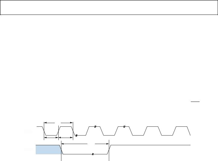
Clock and Reset Timing
Table 16 and Figure 11 describe clock and reset operations. Per Absolute Maximum Ratings on Page 23, combinations of CLKIN and clock multipliers/divisors must not result in core/
Table 16. Clock and Reset Timing
system clocks exceeding the maximum limits allowed for the processor, including system clock restrictions related to supply voltage.
Parameter |
|
|
Min |
Max |
Unit |
Timing Requirements |
|
|
|
||
tCKIN |
CLKIN Period1, 2, 3, 4 |
25.0 |
100.0 |
ns |
|
tCKINL |
CLKIN Low Pulse |
10.0 |
|
ns |
|
tCKINH |
CLKIN High Pulse |
10.0 |
|
ns |
|
tWRST |
|
Asserted Pulse Width Low5 |
11 tCKIN |
|
ns |
RESET |
|
||||
1 Applies to PLL bypass mode and PLL nonbypass mode.
2 CLKIN frequency must not change on the fly.
3Combinations of the CLKIN frequency and the PLL clock multiplier must not exceed the allowed fVCO, fCCLK, and fSCLK settings discussed in Table 12 on Page 24 through
Table 15 on Page 24. Since the default behavior of the PLL is to multiply the CLKIN frequency by 10, the 400 MHz speed grade parts cannot use the full CLKIN period range.
4 If the DF bit in the PLL_CTL register is set, then the maximum tCKIN period is 50 ns.
5Applies after power-up sequence is complete. At power-up, the processor’s internal phase-locked loop requires no more than 2,000 CLKIN cycles, while RESET is asserted, assuming stable power supplies and CLKIN (not including start-up time of external clock oscillator).
tCKIN
CLKIN
tCKINL tCKINH
tWRST
RESET
Figure 11. Clock and Reset Timing
Rev. E | Page 25 of 60 | July 2007
ADSP-BF531/ADSP-BF532/ADSP-BF533
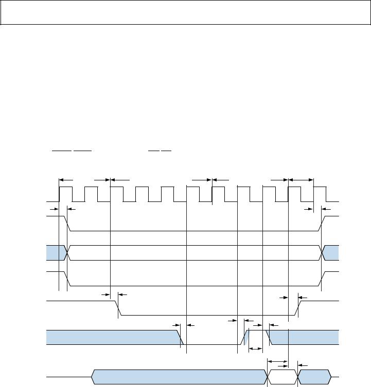
Asynchronous Memory Read Cycle Timing
Table 17. Asynchronous Memory Read Cycle Timing
|
|
VDDEXT = 1.8 V |
VDDEXT = 2.5 V/3.3 V |
|
||
Parameter |
|
Min |
Max |
Min |
Max |
Unit |
Timing Requirements |
|
|
|
|
|
|
tSDAT |
DATA15–0 Setup Before CLKOUT |
2.1 |
|
2.1 |
|
ns |
tHDAT |
DATA15–0 Hold After CLKOUT |
1.0 |
|
0.8 |
|
ns |
tSARDY |
ARDY Setup Before CLKOUT |
4.0 |
|
4.0 |
|
ns |
tHARDY |
ARDY Hold After CLKOUT |
1.0 |
|
0.0 |
|
ns |
Switching Characteristics |
|
|
|
|
|
|
tDO |
Output Delay After CLKOUT1 |
|
6.0 |
|
6.0 |
ns |
tHO |
Output Hold After CLKOUT 1 |
1.0 |
|
0.8 |
|
ns |
1 Output pins include AMS3–0, ABE1–0, ADDR19–1, DATA15–0, AOE, ARE.
|
|
|
HOLD |
SETUP |
PROGRAMMED READ ACCESS |
ACCESS EXTENDED |
1 CYCLE |
|
|||
2 CYCLES |
4 CYCLES |
3 CYCLES |
|
CLKOUT |
|
|
|
tDO |
|
|
tHO |
AMSx |
|
|
|
ABE1–0 |
ABE, ADDRESS |
|
|
|
|
|
|
ADDR19–1 |
|
|
|
AOE |
|
|
|
|
tDO |
|
tHO |
|
|
|
|
ARE |
|
|
|
|
tHARDY |
|
tHARDY |
|
tSARDY |
|
|
ARDY |
|
|
|
|
|
tSARDY |
tSDAT |
|
|
|
|
|
|
|
tHDAT |
DATA15–0 |
|
|
READ |
Figure 12. Asynchronous Memory Read Cycle Timing
Rev. E | Page 26 of 60 | July 2007
ADSP-BF531/ADSP-BF532/ADSP-BF533
Asynchronous Memory Write Cycle Timing
Table 18. Asynchronous Memory Write Cycle Timing
|
|
VDDEXT = 1.8 V |
VDDEXT = 2.5 V/3.3 V |
|
||
Parameter |
|
Min |
Max |
Min |
Max |
Unit |
Timing Requirements |
|
|
|
|
|
|
tSARDY |
ARDY Setup Before CLKOUT |
4.0 |
|
4.0 |
|
ns |
tHARDY |
ARDY Hold After CLKOUT |
1.0 |
|
0.0 |
|
ns |
Switching Characteristics |
|
|
|
|
|
|
tDDAT |
DATA15–0 Disable After CLKOUT |
|
6.0 |
|
6.0 |
ns |
tENDAT |
DATA15–0 Enable After CLKOUT |
1.0 |
|
1.0 |
|
ns |
tDO |
Output Delay After CLKOUT1 |
|
6.0 |
|
6.0 |
ns |
tHO |
Output Hold After CLKOUT 1 |
1.0 |
|
0.8 |
|
ns |
1 Output pins include AMS3–0, ABE1–0, ADDR19–1, DATA15–0, AOE, AWE.
SETUP |
PROGRAMMED WRITE |
ACCESS |
HOLD |
||||
EXTENDED |
|||||||
2 CYCLES |
|
ACCESS 2 CYCLES |
1 CYCLE |
1 CYCLE |
|||
|
|
|
|
|
|
|
|
CLKOUT |
|
tDO |
tHO |
AMSx |
|
ABE1–0 |
|
ABE, ADDRESS |
|
ADDR19–1 |
|
tDO |
tHO |
|
|
AWE |
|
tSARDY |
tHARDY |
ARDY |
|
|
|
|
|
|
tENDAT |
tSARDY |
|
|
|
|
|
tDDAT |
|
|
|
|
|
|
|||||||
DATA15–0 |
|
|
WRITE DATA |
|
|
|
||||||
|
|
|
|
|
|
|
||||||
|
|
|
|
|
|
|
|
|
|
|
|
|
Figure 13. Asynchronous Memory Write Cycle Timing
Rev. E | Page 27 of 60 | July 2007