

ADSP-BF531/ADSP-BF532/ADSP-BF533
SPECIFICATIONS
Component specifications are subject to change without notice.
OPERATING CONDITIONS
Parameter |
Conditions |
Min |
Nominal |
Max |
Unit |
|
|
|
|
|
|
|
|
VDDINT |
Internal Supply Voltage1 |
Nonautomotive 400 MHz and 500 MHz speed grade models2 |
0.8 |
1.2 |
1.32 |
V |
VDDINT |
Internal Supply Voltage1 |
Nonautomotive 533 MHz speed grade models2 |
0.8 |
1.25 |
1.375 |
V |
VDDINT |
Internal Supply Voltage1 |
600 MHz speed grade models2 |
0.8 |
1.30 |
1.45 |
V |
VDDINT |
Internal Supply Voltage1 |
Automotive grade models2 |
0.95 |
1.2 |
1.32 |
V |
VDDEXT |
External Supply Voltage |
Nonautomotive grade models2 |
1.75 |
1.8/2.5/3.3 |
3.6 |
V |
VDDEXT |
External Supply Voltage |
Automotive grade models2 |
2.7 |
3.3 |
3.6 |
V |
VDDRTC |
Real-Time Clock |
Nonautomotive grade models2 |
1.75 |
1.8/2.5/3.3 |
3.6 |
V |
|
Power Supply Voltage |
|
|
|
|
|
VDDRTC |
Real-Time Clock |
Automotive grade models2 |
2.7 |
3.3 |
3.6 |
V |
|
Power Supply Voltage |
|
|
|
|
|
VIH |
High Level Input Voltage3, 4 |
VDDEXT =1.85 V |
1.3 |
|
3.6 |
V |
VIH |
High Level Input Voltage3, 4 |
VDDEXT =Maximum |
2.0 |
|
3.6 |
V |
VIHCLKIN |
High Level Input Voltage5 |
VDDEXT =Maximum |
2.2 |
|
3.6 |
V |
VIL |
Low Level Input Voltage3, 6 |
VDDEXT =1.75 V |
–0.3 |
|
+0.3 |
V |
VIL |
Low Level Input Voltage3, 6 |
VDDEXT =2.25 V |
–0.3 |
|
+0.6 |
V |
TJ |
Junction Temperature |
160-Ball Chip Scale Ball Grid Array (CSP_BGA) @ TAMBIENT = 0°C to +70°C |
0 |
|
+95 |
°C |
TJ |
Junction Temperature |
160-Ball Chip Scale Ball Grid Array (CSP_BGA) @ TAMBIENT = –40°C to +85°C |
–40 |
|
+105 |
°C |
TJ |
Junction Temperature |
160-Ball Chip Scale Ball Grid Array (CSP_BGA) @ TAMBIENT = –40°C to +105°C |
–40 |
|
+125 |
°C |
TJ |
Junction Temperature |
169-Ball Plastic Ball Grid Array (PBGA) @ TAMBIENT = –40°C to +105°C |
–40 |
|
+125 |
°C |
TJ |
Junction Temperature |
169-Ball Plastic Ball Grid Array (PBGA) @ TAMBIENT = –40°C to +85°C |
–40 |
|
+105 |
°C |
TJ |
Junction Temperature |
176-Lead Quad Flatpack (LQFP) @ TAMBIENT = –40°C to +85°C |
–40 |
|
+100 |
°C |
|
|
|
|
|
|
|
1 The regulator can generate VDDINT at levels of 0.85 V to 1.2 V with –5% to +10% tolerance, 1.25 V with–4% to +10% tolerance, and 1.3 V with –0% to +10% tolerance.
2 See Ordering Guide on Page 59.
3 Applies to all input and bidirectional pins except CLKIN.
4The ADSP-BF531/ADSP-BF532/ADSP-BF533 processors are 3.3 V tolerant (always accepts up to 3.6 V maximum VIH), but voltage compliance (on outputs, VOH) depends on the input VDDEXT, because VOH (maximum) approximately equals VDDEXT (maximum). This 3.3 V tolerance applies to bidirectional pins (DATA15–0, TMR2–0, PF15–0, PPI3–0, RSCLK1–0, TSCLK1–0, RFS1–0, TFS1–0, MOSI, MISO, SCK) and input only pins (BR, ARDY, PPI_CLK, DR0PRI, DR0SEC, DR1PRI, DR1SEC, RX, RTXI, TCK, TDI, TMS, TRST, CLKIN, RESET, NMI, and BMODE1–0).
5 Applies to CLKIN pin only.
6 Applies to all input and bidirectional pins.
Rev. E | Page 21 of 60 | July 2007

ADSP-BF531/ADSP-BF532/ADSP-BF533
ELECTRICAL CHARACTERISTICS
|
|
|
|
|
|
Low Power1 |
|
High Speed2 |
|
|
Parameter |
|
|
|
Test Conditions |
Min Typical |
Max |
Min Typical |
Max |
Unit |
|
|
|
|
|
|
|
|
|
|||
VOH |
High Level Output Voltage3 |
@ VDDEXT = 1.75 V, IOH = –0.5 mA |
1.5 |
|
1.5 |
|
V |
|||
VOH |
High Level Output Voltage3 |
@ VDDEXT = 2.25 V, IOH = –0.5 mA |
1.9 |
|
1.9 |
|
V |
|||
VOH |
High Level Output Voltage3 |
@ VDDEXT = 3.0 V, IOH = –0.5 mA |
2.4 |
|
2.4 |
|
V |
|||
VOL |
Low Level Output Voltage3 |
@ VDDEXT = 1.75 V, IOL = 2.0 mA |
|
0.2 |
|
0.2 |
V |
|||
VOL |
Low Level Output Voltage3 |
@ VDDEXT = 2.25 V/3.0 V, IOL = 2.0 mA |
|
0.4 |
|
0.4 |
V |
|||
IIH |
High Level Input Current4 |
@ VDDEXT = Maximum, VIN = VDD Maximum |
|
10.0 |
|
10.0 |
μA |
|||
IIHP |
High Level Input Current JTAG5 |
@ VDDEXT = Maximum, VIN = VDD Maximum |
|
50.0 |
|
50.0 |
μA |
|||
IIL6 |
Low Level Input Current4 |
@ VDDEXT = Maximum, VIN = 0 V |
|
10.0 |
|
10.0 |
μA |
|||
IOZH |
Three-State Leakage Current7 |
@ VDDEXT = Maximum, VIN = VDD Maximum |
|
10.0 |
|
10.0 |
μA |
|||
IOZL6 |
Three-State Leakage Current7 |
@ VDDEXT = Maximum, VIN = 0 V |
|
10.0 |
|
10.0 |
μA |
|||
CIN |
Input Capacitance8 |
fIN = 1 MHz, TAMBIENT = 25°C, VIN = 2.5 V |
4 |
89 |
4 |
89 |
pF |
|||
IDDHIBERNATE |
VDDINT Current in Hibernate State |
VDDEXT = 3.65 V |
50 |
|
50 |
|
μA |
|||
|
|
|
|
|
with voltage regulator off (VDDINT = 0 V) |
|
|
|
|
|
IDDRTC |
VDDRTC Current |
VDDRTC = 3.3 V, TJUNCTION = 25°C |
20 |
|
20 |
|
μA |
|||
|
10 |
VDDINT Current in Deep Sleep Mode |
VDDINT = 0.8 V, TJUNCTION = 25°C |
7.5 |
|
35 |
|
mA |
||
IDDDEEPSLEEP |
|
|
||||||||
IDDSLEEP |
VDDINT Current in Sleep Mode |
VDDINT = 0.8 V, TJUNCTION = 25°C, SCLK = 25 MHz |
10 |
|
37.5 |
|
mA |
|||
|
10, 11 |
VDDINT Current Dissipation (Typical) |
VDDINT = 0.8 V, fCCLK = 50 MHz, TJUNCTION = 25°C |
20 |
|
47 |
|
mA |
||
IDD_TYP |
|
|
||||||||
|
10, 11 |
VDDINT Current Dissipation (Typical) |
VDDINT = 1.14 V, fCCLK = 400 MHz, TJUNCTION = 25°C |
132 |
|
198 |
|
mA |
||
IDD_TYP |
|
|
||||||||
|
10, 11 |
VDDINT Current Dissipation (Typical) |
VDDINT = 1.2 V, fCCLK = 500 MHz, TJUNCTION = 25°C |
|
|
240 |
|
mA |
||
IDD_TYP |
|
|
|
|||||||
|
10, 11 |
VDDINT Current Dissipation (Typical) |
VDDINT = 1.2 V, fCCLK = 533 MHz, TJUNCTION = 25°C |
|
|
250 |
|
mA |
||
IDD_TYP |
|
|
|
|||||||
|
10, 11 |
VDDINT Current Dissipation (Typical) |
VDDINT = 1.3 V, fCCLK = 600 MHz, TJUNCTION = 25°C |
|
|
308 |
|
mA |
||
IDD_TYP |
|
|
|
|||||||
1 |
Applies to all 400 MHz speed grade models. See Ordering Guide on Page 59. |
|
|
|
|
|
||||
2 |
Applies to all 500 MHz, 533 MHz, and 600 MHz speed grade models. See Ordering Guide on Page 59. |
|
|
|
|
|
||||
3 |
Applies to output and bidirectional pins. |
|
|
|
|
|
|
|||
4 |
Applies to input pins except JTAG inputs. |
|
|
|
|
|
|
|||
5 |
Applies to JTAG input pins (TCK, TDI, TMS, |
TRST) |
. |
|
|
|
|
|
|
|
6 |
Absolute value. |
|
|
|
|
|
|
|||
7 |
Applies to three-statable pins. |
|
|
|
|
|
|
|||
8 |
Applies to all signal pins. |
|
|
|
|
|
|
|||
9 |
Guaranteed, but not tested. |
|
|
|
|
|
|
|||
10See Estimating Power for ADSP-BF531/BF532/BF533 Blackfin Processors (EE-229) on the Analog Devices website (www.analog.com)—use site search on “EE-229.” 11Processor executing 75% dual MAC, 25% ADD with moderate data bus activity.
Rev. E | Page 22 of 60 | July 2007
ADSP-BF531/ADSP-BF532/ADSP-BF533
ABSOLUTE MAXIMUM RATINGS
Stresses greater than those listed in the table may cause perma nent damage to the device. These are stress ratings only. Functional operation of the device at these or any other condi tions greater than those indicated in the operational sections of this specification is not implied. Exposure to absolute maximum rating conditions for extended periods may affect device reliability.
PACKAGE INFORMATION
The information presented in Figure 10 and Table 11 provides details about the package branding for the Blackfin processors. For a complete listing of product availability, see the Ordering Guide on Page 59.
Parameter |
Rating |
|
|
Internal (Core) Supply Voltage (VDDINT) |
–0.3 V to +1.4 V |
External (I/O) Supply Voltage (VDDEXT) |
–0.5 V to +3.8 V |
Input Voltage1 |
–0.5 V to +3.8 V |
Output Voltage Swing |
–0.5 V to VDDEXT +0.5 V |
Load Capacitance2 |
200 pF |
Storage Temperature Range |
–65 C to +150°C |
Junction Temperature Under Bias |
125°C |
|
|
1 Applies to 100% transient duty cycle. For other duty cycles see Table 10.
2 For proper SDRAM controller operation, the maximum load capacitance is 50 pF (at 3.3 V) or 30 pF (at 2.5 V) for ADDR19–1, DATA15–0, ABE1–0/SDQM1–0,
CLKOUT, SCKE, SA10, SRAS, SCAS, SWE, and SMS.
Table 10. Maximum Duty Cycle for Input Transient Voltage1
VIN Min (V) |
VIN Max (V)2 |
Maximum Duty Cycle |
–0.50 |
+3.80 |
100% |
–0.70 |
+4.00 |
40% |
–0.80 |
+4.10 |
25% |
–0.90 |
+4.20 |
15% |
–1.00 |
+4.30 |
10% |
|
|
|
1 Applies to all signal pins with the exception of CLKIN, XTAL, VROUT1–0.
2 Only one of the listed options can apply to a particular design.
ESD SENSITIVITY
ESD (electrostatic discharge) sensitive device.
Charged devices and circuit boards can discharge without detection. Although this product features patented or proprietary circuitry, damage may occur on devices subjected to high energy ESD. Therefore, proper ESD precautions should be take to avoid performance degradation or loss of functionality.
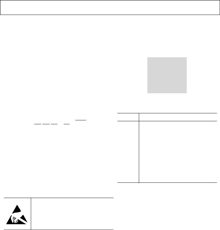
a
ADSP-BF53x
tppZ-cc
vvvvvv.x n.n
yyww country_of_origin
B
Figure 10. Product Information on Package
Table 11. Package Brand Information
Brand Key Field Description
ADSP-BF53x Either ADSP-BF531, ADSP-BF532, or ADSP-BF533
tTemperature Range
pp |
Package Type |
ZRoHS Compliant Part
cc |
See Ordering Guide |
vvvvvv.x |
Assembly Lot Code |
n.nSilicon Revision
yyww |
Date Code |
Rev. E | Page 23 of 60 | July 2007