

TMS320E25
SPRS010B Ð MAY 1987 Ð REVISED NOVEMBER 1990
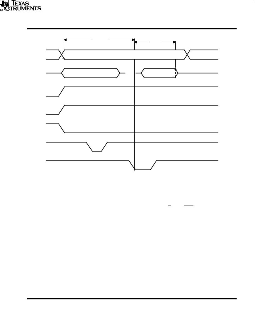
program verify
Programmed bits may be verified with VPP = 12.5 V when G = VIL, E = VIL, and PGM = VIH. Figure 11 shows the timing for the program and verify operation.
Start
Address = First
Location
VCC = 6 ± 0.25 V
VPP = 12.5 V ± 0.25
V
|
X = 0 |
|
|
Program One |
|
|
1-ms Pulse |
|
|
Increment X |
|
No |
|
|
Yes |
Fail |
|
X = 25? |
Verify |
|
One |
|
|
|
|
|
|
Byte |
|
|
Pass |
|
|
Program One |
|
Device |
Pulse of |
|
3X-ms Duration |
|
|
Failed |
|
|
|
|
|
|
No |
Increment |
|
Last |
|
|
Address? |
Address |
|
Yes |
|
|
VCC = VPP = 5 V ± 0.25 V |
|
Fail |
Compare All |
|
|
Bytes to Original |
|
|
Data |
|
Pass
Device
Passed
Figure 10. Fast Programming Flowchart
ADVANCE INFORMATION
POST OFFICE BOX 1443 • HOUSTON, TEXAS 77001 |
61 |
TMS320E25
SPRS010B Ð MAY 1987 Ð REVISED NOVEMBER 1990
INFORMATION ADVANCE
|
|
|
|
|
|
|
Program |
|
|
|
|
|
|
A12-A0 |
|
|
|
|
|
Verify |
VIH |
||||||
|
|
|
|
|
|
||||||||
|
|
|
|
|
|
|
|||||||
|
|
|
|
|
|
|
|||||||
|
|
Address Stable |
|
|
Address N + 1 |
||||||||
|
|
|
|
|
|
|
|
|
|
|
|
|
VIL |
Q8-Q1 |
|
|
|
|
|
|
|
VIH/VOH |
|||||
Data In Stable |
|
HI-Z |
|
Data Out Valid |
|||||||||
|
|
|
|
|
|
|
|
|
|
|
|
|
VIL/VOL |
|
|
|
|
|
|
|
|
|
|
|
|||
|
VPP |
|
|
|
|
|
|
|
VPP |
||||
|
|
|
|
|
|
|
|
VCC |
|||||
|
|
|
|
|
|
|
|
|
|
|
|
|
|
|
VCC |
|
|
|
|
|
|
|
VCC + 1 |
||||
|
|
|
|
|
|
|
|
VCC |
|||||
|
|
|
|
|
|
|
|
|
|
|
|
|
|
|
|
|
|
|
|
|
|
|
|
|
|
|
VIH |
|
|
|
E |
|
|
|
|
|
|
|
|
|
|
|
|
|
|
|
|
|
|
|
|
|
|
|
VIL |
|
|
|
|
|
|
|
|
|
|
|
|
|
VIH |
|
PGM |
|
|
|
|
|
|
|
|
|
|||
|
|
|
|
|
|
|
|
|
|
|
|
|
VIL |
|
|
|
|
|
|
|
|
|
|
|
|
|
VIH |
|
|
G |
|
|
|
|
|
|
|
|
|
||
|
|
|
|
|
|
|
|
|
|
|
|
|
VIL |
Figure 11. Fast Programming Timing
program inhibit
Programming may be inhibited by maintaining a high level input on the E pin or PGM pin.
read
The EPROM contents may be read independent of the programming cycle, provided the RBIT (ROM protect bit) has not been programmed. The read is accomplished by setting E to zero and pulsing G low. The contents of the EPROM location selected by the value on the address inputs appear on Q8-Q1.
output disable
During the EPROM programming process, the EPROM data outputs may be disabled, if desired, by establishing the output disable state. This state is selected by setting the G and PGM pins high. While output disable is selected, Q8-Q1 are placed in the high-impedance state.
ROM protection and verification
This section describes the code protection feature included in the EPROM cell, which protects code against copyright violations. Table 6 shows the programming levels required for protecting and verifying the EPROM. The paragraphs following the table describe the protect and verify functions.
62 |
POST OFFICE BOX 1443 • HOUSTON, TEXAS 77001 |

TMS320E25
SPRS010B Ð MAY 1987 Ð REVISED NOVEMBER 1990
Table 6. TMS320E25 Protect and Verify EPROM Mode Levels
SIGNAL ² |
TMS320E25 PIN |
TMS27C64 PIN |
ROM PROTECT |
PROTECT VERIFY |
|||||||||
|
|
|
|
|
|
|
|
22 |
20 |
VIH |
VIL |
||
|
|
|
E |
|
|
|
|
||||||
|
|
|
|
|
|
|
|
42 |
22 |
VIH |
VIL |
||
|
|
|
G |
|
|
|
|||||||
|
|
|
|
|
|
|
|
41 |
27 |
VIH |
VIH |
||
|
PGM |
|
|||||||||||
|
VPP |
25 |
1 |
VPP |
VCC |
||||||||
|
VCC |
61,35 |
28 |
VCC + 1 |
VCC |
||||||||
|
VSS |
10, 27, 44 |
14 |
VSS |
VSS |
||||||||
CLKIN |
52 |
14 |
VSS |
VSS |
|||||||||
|
|
|
|
|
|
|
|
65 |
14 |
VSS |
VSS |
||
|
|
RS |
|
||||||||||
|
EPT |
24 |
26 |
VPP |
VPP |
||||||||
Q8-Q1 |
18-11 |
11-13, 15-19 |
Q8 = |
|
|
Q8 = RBIT |
|||||||
PULSE |
|
||||||||||||
|
|
|
|
|
|
||||||||
A12-A10 |
40-38 |
2, 23, 21, |
|
X |
X |
||||||||
|
|
|
|
|
|
||||||||
A9-A7 |
37, 36, 34 |
24, 25, 3 |
|
X |
X |
||||||||
|
|
|
|
|
|
|
|
||||||
|
|
A6 |
33 |
4 |
|
X |
VIL |
||||||
|
|
A5 |
32 |
5 |
|
X |
X |
||||||
|
|
|
|
|
|
|
|||||||
|
|
A4 |
31 |
6 |
VIH |
X |
|||||||
A3-A0 |
30-28, 26 |
7-10 |
|
X |
X |
||||||||
² In accordance with TMS27C64.
LEGEND;
VIH = TTL high level; VIL = TTL low level; VCC = 5 V ± 0.25 V
VPP = 12.5 V ± 0.5 V; X = don't care
PULSE = low-going TTL level pulse; RBIT = ROM protect bit.
EPROM protect
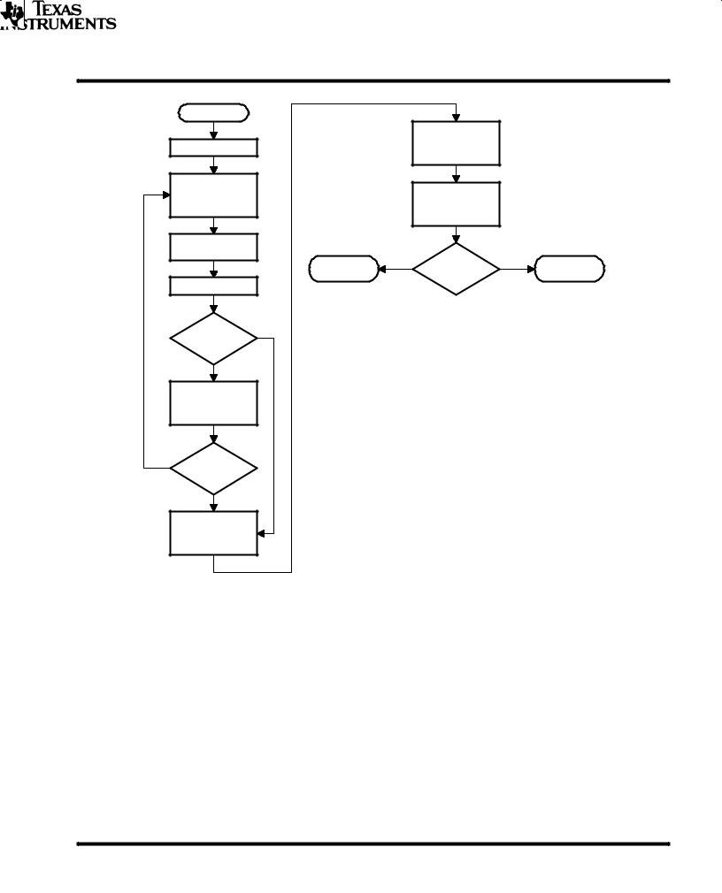
The EPROM protect facility is used to completely disable reading of the EPROM contents to guarantee security of propietary algorithms. This facility is implemented through a unique EPROM cell called the RBIT (EPROM protect bit) cell. Once the contents to be protected are programmed into the EPROM, the RBIT is programmed, disabling access to the EPROM contents and disabling the microprocessor mode on the device. Once programmed, the RBIT can be cleared only by erasing the entire EPROM array with ultraviolet light, thereby maintaining security of the propietary algorithm. Programming the RBIT is accomplished using the EPROM protect cycle, which consists of setting the E, G, PGM, and A4 pins high, VPP and EPT to 2.5 V ± 0.5 V, and pulsing Q8 low. The complete sequence of operations involved in programming the RBIT is shown in the flowchart of Figure 12. The required setups in the figure are detailed in Table 6.
ADVANCE INFORMATION
POST OFFICE BOX 1443 • HOUSTON, TEXAS 77001 |
63 |
TMS320E25
SPRS010B Ð MAY 1987 Ð REVISED NOVEMBER 1990
INFORMATION ADVANCE
Start
|
Program One |
|
X = 0 |
Pulse of 3X-ms |
|
Duration |
|
|
|
|
|
EPROM |
Protect |
|
Protect |
|
|
Setup |
Verify |
|
|
Setup |
|
Program One |
|
|
1-ms Pulse |
|
|
Device |
Verify |
Device |
Failed |
RBIT |
Passed |
X = X + 1
Yes
X = 25?
No
Protect
Verify
Setup
Fail
Verify
RBIT
Pass
EPROM
Protect
Setup
Figure 12. EPROM Protect Flowchart
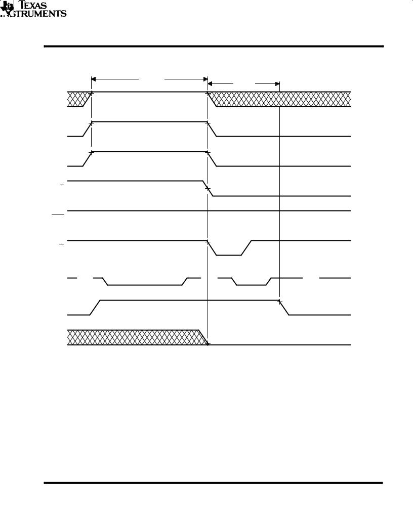
protect verify
Protect verify is used following the EPROM protect to verify correct programming of the RBIT (see Figure 12). When using protect verify, Q8 outputs the state of the RBIT. When RBIT = 1, the EPROM is unprotected; when RBIT = 0, the EPROM is protected. The EPROM protect and verify timings are shown in Figure 13.
64 |
POST OFFICE BOX 1443 • HOUSTON, TEXAS 77001 |
TMS320E25
SPRS010B Ð MAY 1987 Ð REVISED NOVEMBER 1990
Protect
Verify
VIH
A4
VIL
VPP
VPP
VCC
VCC + 1
VCC
VCC
VIH
E
VIL
VIH
PGM
VIL
VIH
G
VIL
VIH/VOH
Q8 |
HI-Z |
|
HI-Z |
|
HI-Z |
VIL/VOL
VPP
EPT
VSS
VIH
A6
VIL
Figure 13. EPROM Protect Timing
ADVANCE INFORMATION
POST OFFICE BOX 1443 • HOUSTON, TEXAS 77001 |
65 |

TMS320 SECOND-GENERATION |
INDEX |
DEVICES |
|
SPRS010B Ð MAY 1987 Ð REVISED NOVEMBER 1990 |
|
|
|
INFORMATION ADVANCE
66 |
POST OFFICE BOX 1443 • HOUSTON, TEXAS 77001 |

NIL
NIL
NIL
SPRS010B Ð MAY 1987 Ð REVISED NOVEMBER 1990
accumulator . . . . . . . . . . . . . . . . . . . . . . . . . . . . . . . 5 adapter socket . . . . . . . . . . . . . . . . . . . . . . . . . . . . 58 addressing modes . . . . . . . . . . . . . . . . . . . . . . . . . 10 ALU . . . . . . . . . . . . . . . . . . . . . . . . . . . . . . . . . . . . . . . 5 architecture . . . . . . . . . . . . . . . . . . . . . . . . . . . . . . . . 5
BIT instruction . . . . . . . . . . . . . . . . . . . . . . . . . . . . . 17 block diagram . . . . . . . . . . . . . . . . . . . . . . . . . . . . . . 6 Bulletin board Service . . . . . . . . . . . . . . . . . . . . . . 18
clock
TMS32020 . . . . . . . . . . . . . . . . . . . . . . . . . . . . . 22 TMS320C25/E25 . . . . . . . . . . . . . . . . . . . . . 28, 29 TMS320C25-50 . . . . . . . . . . . . . . . . . . . . . . 35, 36
description . . . . . . . . . . . . . . . . . . . . . . . . . . . . . . . . . 1 development support . . . . . . . . . . . . . . . . . . . . 18, 19 direct addressing . . . . . . . . . . . . . . . . . . . . . . . 10, 17 DMA documentation support . . . . . . . . . . . . . . . . 20
EPROM protection/verification . . . . . . . . . . . . 58-65 external interface . . . . . . . . . . . . . . . . . . . . . . . . . . . 9
flowcharts
EPROM protect . . . . . . . . . . . . . . . . . . . . . . . . . 63 fast . . . . . . . . . . . . . . . . . . . . . . . . . . . . . . . . . 60, 61
hotline . . . . . . . . . . . . . . . . . . . . . . . . . . . . . . . . . . . . 18 immediate addressing . . . . . . . . . . . . . . . . . . . . . . 10 indirect addressing . . . . . . . . . . . . . . . . . . . . . . 10, 17 instruction set . . . . . . . . . . . . . . . . . . . . . . . . . . 10-16 interrupts . . . . . . . . . . . . . . . . . . . . . . . . . . . . . . . . . . 9 introduction . . . . . . . . . . . . . . . . . . . . . . . . . . . . . . . . 3
key features
TMS320 family . . . . . . . . . . . . . . . . . . . . . . . . . . . 1 TMS32020 . . . . . . . . . . . . . . . . . . . . . . . . . . . . . . 4 TMS320C25/C25-50/E25 . . . . . . . . . . . . . . . . . . 4
mechanical data
TMS32020 . . . . . . . . . . . . . . . . . . . . . . . . . . . . . 55 TMS320C25 . . . . . . . . . . . . . . . . . . . . . . . . . 55, 56 TMS320C25-50 . . . . . . . . . . . . . . . . . . . . . . . . . 56 TMS320E25 . . . . . . . . . . . . . . . . . . . . . . . . . . . . 57
memory
addressing modes . . . . . . . . . . . . . . . . . . . . 10, 17 control . . . . . . . . . . . . . . . . . . . . . . . . . . . . . . . . . . 7 maps . . . . . . . . . . . . . . . . . . . . . . . . . . . . . . . . . . . 8
microcomputer/microprocessor mode
multiplier . . . . . . . . . . . . . . . . . . . . . . . . . . . . . . . . . . 7 multiprocessing . . . . . . . . . . . . . . . . . . . . . . . . . . . . . 9
operation conditions
TMS32020 . . . . . . . . . . . . . . . . . . . . . . . . . . 17, 21 TMS320C25 . . . . . . . . . . . . . . . . . . . . . . . . . . . . 27 TMS320C25-50 . . . . . . . . . . . . . . . . . . . . . . . . . 34 TMS320E25 . . . . . . . . . . . . . . . . . . . . . . . . . 27, 33 overflow . . . . . . . . . . . . . . . . . . . . . . . . . . . . . . . . . . 17
overview
TMS320 . . . . . . . . . . . . . . . . . . . . . . . . . . . . . . . . 5 specification . . . . . . . . . . . . . . . . . . . . . . . . . . . . 20
package types . . . . . . . . . . . . . . . . . . . . . . . . . . . |
. 1-5 |
pin assignments . . . . . . . . . . . . . . . . . . . . . . . . . . |
. . 2 |
pin nomenclature |
|
TMS32020/C25/C25-50 . . . . . . . . . . . . . . . . . |
. . 2 |
TMS320E25 . . . . . . . . . . . . . . . . . . . . . . . . . . . |
. 60 |
pinouts |
|
TMS32020/C25/C25-50 . . . . . . . . . . . . . . . . . |
. . 1 |
TMS320E25 . . . . . . . . . . . . . . . . . . . . . . . . . . . |
. 60 |
programming levels for EPROM . . . . . . . . . . |
58-65 |
repeat feature . . . . . . . . . . . . . . . . . . . . . . . . . . . . |
. 10 |
reflow soldering precaution . . . . . . . . . . . . . . . . . |
. 54 |
serial port . . . . . . . . . . . . . . . . . . . . . . . . . . . . . . . . 7, 9 shifter . . . . . . . . . . . . . . . . . . . . . . . . . . . . . . . . . . . . . 7 specification overview . . . . . . . . . . . . . . . . . . . . . . 20 subroutines . . . . . . . . . . . . . . . . . . . . . . . . . . . . . . . . 9 supply current characteristics . . . . . . . . . . . . . . . . 54 switching characteristics
TMS32020 . . . . . . . . . . . . . . . . . . . . . . . 21, 23-26 TMS320C25/E25 . . . . . . . . . . . . . . . . . . 27, 28-33 TMS320C25-50 . . . . . . . . . . . . . . . . . . . 34, 35-40
timer . . . . . . . . . . . . . . . . . . . . . . . . . . . . . . . . . . . . . . 7 timing diagrams . . . . . . . . . . . . . . . . . . 41-53, 62, 65 TMS320 Second-Generation . . . . . . . . . . . 41-47 TMS32020 . . . . . . . . . . . . . . . . . . . 46, 48, 50, 51 TMS320C25/E25 . . . . . . . . . . . . . . 46, 49, 52, 53
TMS3220 product notification . . . . . . . . . . . . . 17
POST OFFICE BOX 1443 • HOUSTON, TEXAS 77001 |
67 |
IMPORTANT NOTICE
Texas Instruments and its subsidiaries (TI) reserve the right to make changes to their products or to discontinue any product or service without notice, and advise customers to obtain the latest version of relevant information to verify, before placing orders, that information being relied on is current and complete. All products are sold subject to the terms and conditions of sale supplied at the time of order acknowledgement, including those pertaining to warranty, patent infringement, and limitation of liability.
TI warrants performance of its semiconductor products to the specifications applicable at the time of sale in accordance with TI's standard warranty. Testing and other quality control techniques are utilized to the extent TI deems necessary to support this warranty. Specific testing of all parameters of each device is not necessarily performed, except those mandated by government requirements.
CERTAIN APPLICATIONS USING SEMICONDUCTOR PRODUCTS MAY INVOLVE POTENTIAL RISKS OF DEATH, PERSONAL INJURY, OR SEVERE PROPERTY OR ENVIRONMENTAL DAMAGE (ªCRITICAL APPLICATIONSº). TI SEMICONDUCTOR PRODUCTS ARE NOT DESIGNED, AUTHORIZED, OR WARRANTED TO BE SUITABLE FOR USE IN LIFE-SUPPORT DEVICES OR SYSTEMS OR OTHER CRITICAL APPLICATIONS. INCLUSION OF TI PRODUCTS IN SUCH APPLICATIONS IS UNDERSTOOD TO BE FULLY AT THE CUSTOMER'S RISK.
In order to minimize risks associated with the customer's applications, adequate design and operating safeguards must be provided by the customer to minimize inherent or procedural hazards.
TI assumes no liability for applications assistance or customer product design. TI does not warrant or represent that any license, either express or implied, is granted under any patent right, copyright, mask work right, or other intellectual property right of TI covering or relating to any combination, machine, or process in which such semiconductor products or services might be or are used. TI's publication of information regarding any third party's products or services does not constitute TI's approval, warranty or endorsement thereof.
Copyright 1998, Texas Instruments Incorporated