

TMS32020
SPRS010B Ð MAY 1987 Ð REVISED NOVEMBER 1990
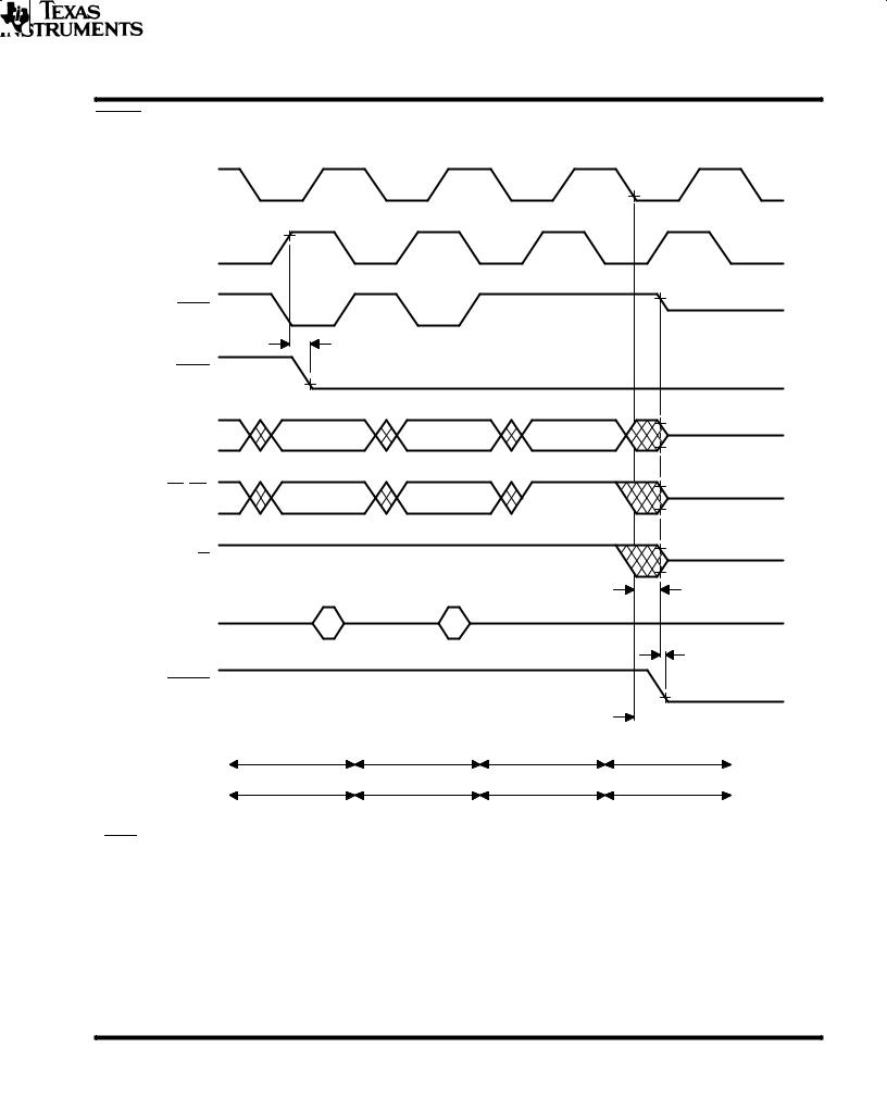
HOLD timing (part B)
CLKOUT1
CLKOUT2
ten(A-C1L)
STRB
 td(C2H-H)²
HOLD
A15-A0 |
Valid |
Valid |
PS, DS, or IS
R/W |
In |
In |

 td(HH-AH)
D15-D0
HOLDA |
|
N + |
2 |
N + 3 |
N/A |
N /A |
N + 2 |
|
N + 3 |
FETCH |
|
|
|
|
Dead |
Dead |
N + 1 |
N + 2 |
|
EXECUTE
ADVANCE INFORMATION
²HOLD is an asynchronous input and can occur at any time during a clock cycle. If the specified timing is met, the exact sequence shown will occur; otherwise, a delay of one CLKOUT2 cycle will occur.
POST OFFICE BOX 1443 • HOUSTON, TEXAS 77001 |
51 |
TMS320C25
INFORMATION ADVANCE
SPRS010B Ð MAY 1987 Ð REVISED NOVEMBER 1990
HOLD timing (part A)
CLKOUT1 |
|
|
|
CLKOUT2 |
|
|
|
STRB |
|
|
|
|
td(C2H-H)² |
|
|
HOLD |
|
|
|
A15-A0 |
N |
N + 1 |
N + 2 |
PS, DS, |
Valid |
Valid |
|
or IS |
|
||
|
|
|
|
R/W |
|
|
|
|
|
|
tdis(C1L-A) |
D15-D0 |
In |
In |
|
|
|
|
tdis(AL-A) |
HOLDA
 td(C1L-AL)
N |
N + 1 |
± |
± |
FETCH |
|
|
|
N ± 2 |
N ± 1 |
N |
± |
EXECUTE |
|
|
|
²HOLD is an asynchronous input and can occur at any time during a clock cycle. If the specified timing is met, the exact sequence shown will occur; otherwise, a delay of one CLKOUT2 cycle will occur.
52 |
POST OFFICE BOX 1443 • HOUSTON, TEXAS 77001 |
TMS320C25
SPRS010B Ð MAY 1987 Ð REVISED NOVEMBER 1990
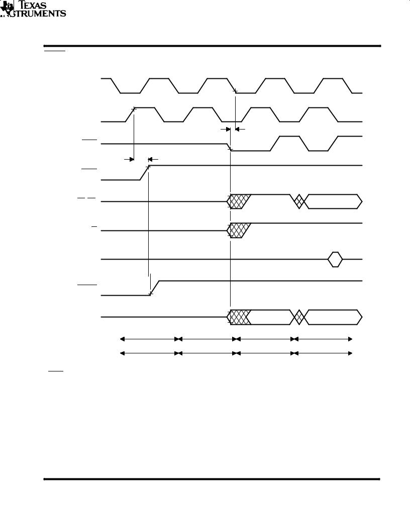
HOLD timing (part B)
CLKOUT1 |
|
CLKOUT2 |
|
|
ten(A-C1L) |
STRB |
|
|
td(C2H-H)² |
HOLD |
|
PS, DS, |
Valid |
or IS |
|
R/W |
|
D15-D0 |
In |

 td(HH-AH)
HOLDA
A15-A0 |
|
N + 2 |
N + 2 |
± |
± |
± |
N + 2 |
FETCH |
|
|
|
± |
± |
± |
N + 1 |
EXECUTE
ADVANCE INFORMATION
²HOLD is an asynchronous input and can occur at any time during a clock cycle. If the specified timing is met, the exact sequence shown will occur; otherwise, a delay of one CLKOUT2 cycle will occur.
POST OFFICE BOX 1443 • HOUSTON, TEXAS 77001 |
53 |
INFORMATION ADVANCE
TMS320 SECOND-GENERATION
DEVICES
SPRS010B Ð MAY 1987 Ð REVISED NOVEMBER 1990
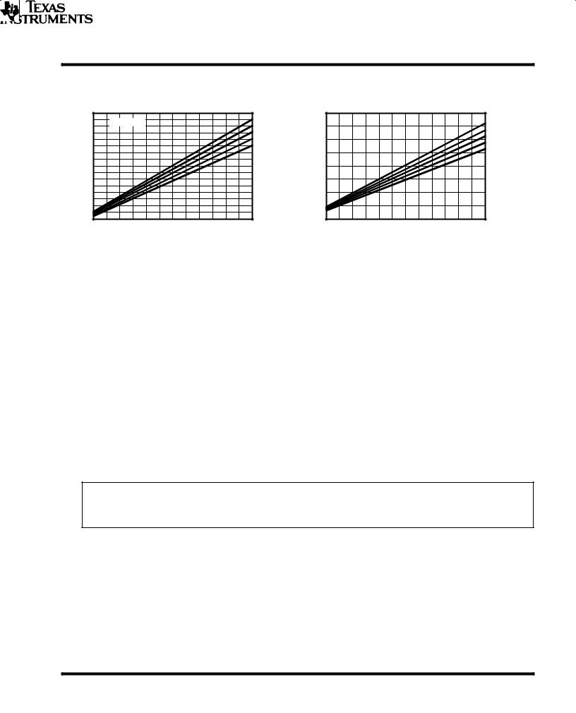
TYPICAL SUPPLY CURRENT CHARACTERISTICS FOR TMS320C25
ICC vs f(CLKIN) and VCC |
ICC vs f(CLKIN) and VCC |
Normal Operating Mode |
Powerdown Mode |
ICC, mA
170
160 TA = 25°C
150
140
130
120
110
100
90
80
70
60
50
40
30
20
10
4 |
8 |
12 |
16 |
20 |
24 |
28 |
32 |
36 |
40 |
44 |
48 |
52 |
f(CLKIN), MHz
VCC = 5.50 V VCC = 5.25 V VCC = 5.00 V VCC = 4.75 V VCC = 4.50 V
ICC, mA
80
70
60
50
40
30
20
10
0
4 |
8 |
12 |
16 |
20 |
24 |
28 |
32 |
36 |
40 |
44 |
48 |
52 |
f(CLKIN), MHz
VCC = 5.50 V VCC = 5.25 V VCC = 5.00 V VCC = 4.75 V VCC = 4.50 V
TMS320C25FNL (PLCC) reflow soldering precautions
Recent tests have identified an industry-wide problem experienced by surface mounted devices exposed to reflow soldering temperatures. This problem involves a package cracking phenomenon sometimes experienced by large (e.g., 68-lead) plastic leaded chip carrier (PLCC) packages during surface mount manufacturing. This phenomenon occur if the TMS320C25FNL is exposed to uncontrolled levels of humidity prior to reflow solder. This moisture can flash to steam during solder reflow, causing sufficient stress to crack the package and compromise device integrity. If the TMS320C25FNL is being socketed, no special handling precautions are required. In addition, once the device is soldered into the board, no special handling precautions are required.
In order to minimize moisture absorption, TI ships the TMS320C25FNL in ªdry packº shipping bags with a RH indicator card and moisture-absorbing desiccant. These moisture-barrier shipping bags will adequately block moisture transmission to allow shelf storage for 12 months from date of seal when stored at less than 60% relative humidity (RH) and less than 30°C. Devices may be stored outside the sealed bags indefinitely if stored at less than 25% RH and 30°C.
Once the bag seal is broken, the devices should be stored at less than 60% RH and 30°C as well as reflow soldered within two days of removal. In the event that either of the above conditions is not met, TI recommends these devices be baked in a clean oven at 125°C and 10% maximum RH for 24 hours. This restores the devices to their ªdry packedº moisture level.
NOTE
Shipping tubes will not withstand the 125°C baking process. Devices should be transferred to a metal tray or tube before baking. Standard ESD precautions should be followed.
In addition, TI recommends that the reflow process not exceed two solder cycles and the temperature not exceed 220°C.
If you have any additional questions or concerns, please contact your local TI representative.
54 |
POST OFFICE BOX 1443 • HOUSTON, TEXAS 77001 |
TMS320 SECOND-GENERATION
DEVICES
SPRS010B Ð MAY 1987 Ð REVISED NOVEMBER 1990
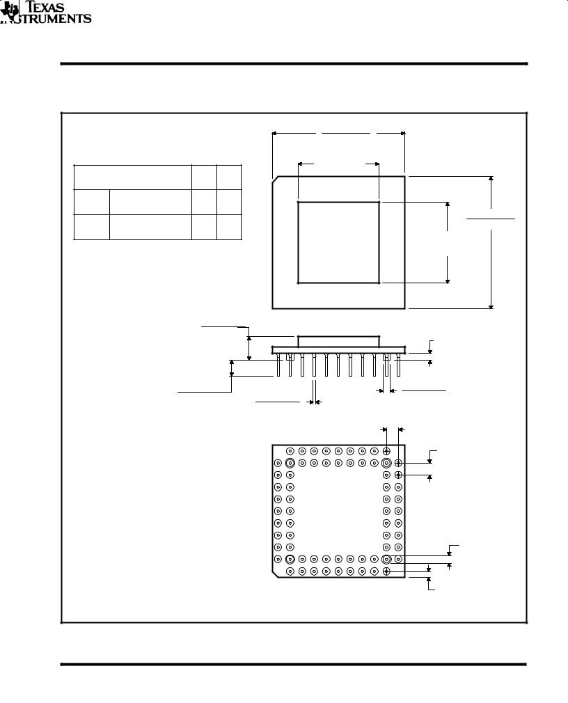
MECHANICAL DATA
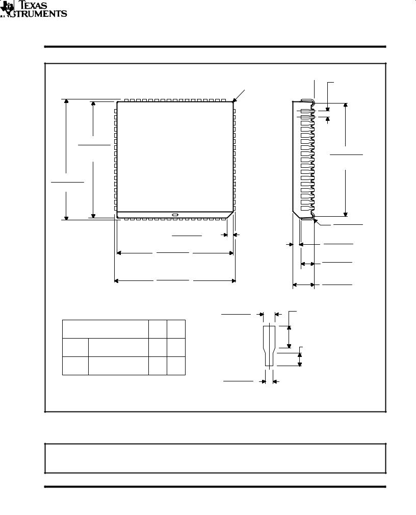
68-pin GB grid array ceramic package (TMS32020, TMS320C25)
|
|
|
|
|
|
|
|
28,448 (1.120) |
|
|
|
|
|
|
|||
|
|
|
|
|
|
|
|
27,432 (1.080) |
|
|
|
|
|
|
|||
Thermal Resistance Characteristics |
|
|
|
|
|
17,02 (0.670) |
|
|
|
|
|
|
|||||
|
|
|
|
|
|
|
|
|
|
|
|
|
|
||||
|
|
|
|
|
|
|
|
|
Nom |
|
|
|
|
|
|
|
|
|
PARAMETER |
MAX |
UNIT |
|
|
|
|
|
|
|
|
|
|
|
|
|
|
RθJA |
Junction-to-free-air |
36 |
°C/W |
|
|
|
|
|
|
|
|
|
|
|
|
|
|
thermal resistance |
|
|
|
|
|
|
|
|
|
|
|
|
28,448 (1.120) |
|
|||
|
|
|
|
|
|
|
|
|
|
|
|
|
|
|
|
|
|
RθJC |
Junction-to-case |
6 |
°C/W |
|
|
|
|
|
|
|
|
|
|
|
|
27,432 (1.080) |
|
thermal resistance |
|
|
|
|
|
|
|
|
|
|
|
17,02 |
|
||||
|
|
|
|
|
|
|
|
|
|
|
|
|
|
|
|
||
|
|
|
|
|
|
|
|
|
|
|
|
|
|
|
(0.670) |
|
|
|
|
|
|
|
|
|
|
|
|
|
|
|
|
|
Nom |
|
|
|
|
4,953 (0.195) |
|
|
|
|
|
|
|
|
|
|
|
|
|
INFORMATION |
|
|
|
2,032 (0.080) |
|
|
|
|
|
|
|
|
|
|
|
1,397 (0.055) |
|||
|
|
|
|
|
|
|
|
|
|
|
|
|
|
|
|||
|
|
|
|
|
|
|
|
|
|
|
|
|
|
|
Max |
||
|
|
|
|
|
|
|
|
|
|
|
|
|
|
|
|
|
|
|
3,302 (0.130) |
|
|
|
|
|
|
|
|
|
1,575 (0.062) |
Dia |
ADVANCE |
||||
|
2,794 (0.110) |
0,508 (0.020) |
|
|
|
|
|
|
|
1,473 (0.058) |
|||||||
|
|
|
|
0,406 (0.016) |
|
|
|
|
|
|
|
|
|
|
|
||
|
|
|
|
|
|
|
|
|
|
|
|
|
|
2,54 |
|
|
|
|
|
|
|
|
|
|
|
|
|
|
|
|
|
(0.100) |
|
||
|
|
|
|
L |
|
|
|
|
|
|
|
|
|
T.P. |
2,54 |
||
|
|
|
|
|
|
|
|
|
|
|
|
|
|
||||
|
|
|
|
K |
|
|
|
|
|
|
|
|
|
|
(0.100) |
||
|
|
|
|
|
|
|
|
|
|
|
|
|
|
T.P. |
|||
|
|
|
|
|
|
|
|
|
|
|
|
|
|
|
|||
|
|
|
|
J |
|
|
|
|
|
|
|
|
|
|
|
||
|
|
|
|
|
|
|
|
|
|
|
|
|
|
|
|
|
|
|
|
|
|
H |
|
|
|
|
|
|
|
|
|
|
|
|
|
|
|
|
|
G |
|
|
|
|
|
|
|
|
|
|
|
|
|
|
|
|
|
F |
|
|
|
|
|
|
|
|
|
|
|
|
|
|
|
|
|
E |
|
|
|
|
|
|
|
|
|
|
|
|
|
|
|
|
|
D |
|
|
|
|
|
|
|
|
|
|
|
|
|
|
|
|
|
C |
|
|
|
|
|
|
|
|
|
|
|
1,524 (0.060) |
|
|
|
|
|
|
|
|
|
|
|
|
|
|
|
|
Nom |
|
|
|
|
|
|
B |
|
|
|
|
|
|
|
|
|
|
|
|
|
|
|
|
|
|
|
|
|
|
|
|
|
|
|
|
4 Places |
|
|
|
|
|
|
A |
|
|
|
|
|
|
|
|
|
|
|
|
|
|
|
|
|
1 |
2 |
3 |
4 |
5 |
6 |
7 |
8 |
9 |
10 11 |
|
1,27 |
|
|
|
|
|
|
|
|
|
|
|
|
|
|
|
|
|
|
||
|
|
|
|
|
|
|
|
|
|
|
|
|
|
|
(0.050) |
|
|
|
|
|
|
|
|
|
|
|
|
|
|
|
|
|
Nom |
|
|
|
ALL LINEAR DIMENSIONS ARE IN MILLIMETERS AND PARENTHETICALLY IN INCHES |
|
|
||||||||||||||
POST OFFICE BOX 1443 • HOUSTON, TEXAS 77001 |
55 |
TMS320C25
TMS320C25-50
SPRS010B Ð MAY 1987 Ð REVISED NOVEMBER 1990
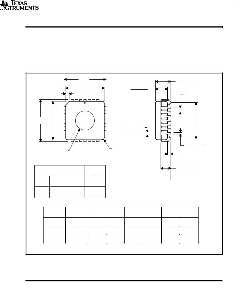
68-lead plastic leaded chip carrier package (TMS320C25 and TMS320C25-50)
|
|
|
|
|
|
Seating |
|
|
|
|
|
|
|
Plane |
1,27 (0.050) T.P. |
|
|
|
|
|
|
|
|
|
|
|
|
|
0,25 (0.010) R Max |
|
(see Note B) |
|
|
|
|
|
|
|
|
|
|
|
|
|
3 Places |
|
|
|
24,33 (0.956) |
|
|
|
|
|
|
|
24,13 (0.950) |
|
|
|
|
23,62 (0.930) |
|
|
(see Note A) |
|
|
|
|
||
|
|
|
|
|
23,11 (0.910) |
||
|
|
|
|
|
|
|
|
|
|
|
|
|
|
|
(At Seating Plane) |
|
25,27 (0.995) |
|
|
|
|
|
|
|
25,02 (0.985) |
|
|
|
|
|
|
ADVANCE |
|
|
|
|
|
|
0,94 (0.037) |
|
|
|
1,22 (0.048) |
|
|
0,69 (0.027) R |
|
|
|
|
×45° |
|
|
||
|
|
|
1,07 (0.042) |
|
1,35 (0.053) |
||
|
|
24,33 (0.956) |
|
|
1,19 (0.047) ×45° |
||
INFORMATION |
|
|
24,13 (0.950) |
|
|
2,79 (0.110) |
|
|
|
(see Note A) |
|
|
|||
|
|
|
|
2,41 (0.095) |
|||
|
|
|
|
|
|
||
|
|
25,27 (0.995) |
|
|
4,50 (0.177) |
||
|
|
25,02 (0.985) |
|
|
|||
|
|
|
|
4,24 (0.167) |
|||
|
|
|
|
|
|
||
Thermal Resistance Characteristics |
0,81 (0.032) |
1,52 (0.060) |
|||||
0,66 (0.026) |
Min |
|
|||||
|
|
|
|
|
|||
|
PARAMETER |
MAX |
UNIT |
|
|
|
|
RθJA |
Junction-to-free-air |
46 |
°C/W |
|
0,64 (0.025) |
||
|
|
||||||
|
thermal resistance |
|
|||||
|
|
Min |
|
||||
|
|
|
|
|
|
|
|
|
RθJC |
Junction-to-case |
11 |
°C/W |
|
|
|
|
thermal resistance |
|
|
|
|||
|
|
|
|
|
0,51 (0.020) |
|
|
|
|
|
|
|
0,36 (0.014) |
|
|
|
|
|
|
|
Lead Detail |
|
|
|
|
ALL LINEAR DIMENSIONS ARE IN MILLIMETERS AND PARENTHETICALLY IN INCHES |
|||||
NOTES: A. Centerline of center pin, each side, is within 0,10 (0.004) of package centerline as determined by this dimension.
B. Location of each pin is within 0,127 (0.005) of true position with respect to center pin on each side.
WARNING
When reflow soldering is required, refer to page 54 for special handling instructions.
56 |
POST OFFICE BOX 1443 • HOUSTON, TEXAS 77001 |
TMS320E25
SPRS010B Ð MAY 1987 Ð REVISED NOVEMBER 1990
MECHANICAL DATA
68-lead FZ CER-QUAD, ceramic leaded chip carrier package (TMS320E25 only)
This hermetically-sealed chip carrier package consists of a ceramic base, ceramic cap, and a 68-lead frame. Hermetic sealing is accomplished with glass. The FZ package is intended for both socketor surfacemounting. Having a Sn/Pb ratio of 60/40, the tin/lead-coated leads do not require special cleaning or processing when being surface-mounted.
A |
4,57 (0.180) |
(see Note 2) |
3,94 (0.155) |
B |
3,55 (0.140) |
1,02 (0.040) × 45° |
3,05 (0.120) |
1,27 (0.050) Typ |
(see Note 3)
A |
|
|
|
|
|
|
|
|
C |
|
B |
|
|
|
|
|
|
|
(At Seating |
||
(see Note 2) |
|
|
|
|
0,81 (0.032) |
|
|
|||
|
|
|
|
|
|
|
|
Plane) |
||
|
|
|
|
|
|
0,66 (0.026) |
|
|
|
|
|
|
|
|
|
|
|
|
|
0,51 (0.020) |
|
(see Note 1) |
|
|
|
0,64 (0.025) |
|
|
0,36 (0.014) |
|||
|
|
|
|
|
|
|||||
|
|
|
R |
|
|
|
|
|||
|
|
|
|
|
|
|
|
1,016 (0.040) Min |
||
|
|
|
|
|
Max |
|
|
|
||
|
|
|
|
|
|
|
|
Ref |
||
|
|
|
|
|
3 Places |
|
|
|||
|
|
|
|
|
|
|
|
|||
Thermal Resistance Characteristics |
|
|
|
|
3,05 (0.120) |
|||||
|
|
|
|
|
|
|
|
|
||
|
PARAMETER |
|
MAX |
UNIT |
|
|
|
|
2,29 (0.090) |
|
RθJA |
Junction-to-free-air |
49 |
°C/W |
|
|
|
Seating Plane |
|||
thermal resistance |
|
|
|
|||||||
|
|
|
|
|
|
|
|
(see Note 4) |
||
RθJC |
Junction-to-case |
8 |
°C/W |
|
|
|
|
|
||
thermal resistance |
|
|
|
|
|
|||||
|
JEDEC |
NO. OF |
|
A |
|
|
B |
|
C |
|
|
|
|
|
|
|
|
|
|||
OUTLINE TERMINALS |
MIN |
MAX |
MIN |
MAX |
MIN |
MAX |
||||
MO-087AA |
28 |
|
12,32 |
12,57 |
10,92 |
11,56 |
10,41 |
10,92 |
||
(0.485) |
(0.465) |
(0.430) |
(0.455) |
(0.410) |
(0.430) |
|||||
|
|
|
||||||||
MO-087AB |
44 |
|
17,40 |
17,65 |
16,00 |
16,64 |
15,49 |
16,00 |
||
(0.685) |
(0.695) |
(0.630) |
(0.655) |
(0.610) |
(0.630) |
|||||
|
|
|
||||||||
|
±±± |
68 |
|
25,02 |
25,27 |
23,62 |
24,26 |
23,11 |
23,62 |
|
|
(0.985) |
(0.995) |
(0.930) |
(0.955) |
(0.910) |
(0.930) |
||||
|
|
|
||||||||
ALL LINEAR DIMENSIONS ARE IN MILLIMETERS AND PARENTHETICALLY IN INCHES
NOTES: 1. Glass is optional, and the diameter is dependent on device application.
2.Centerline of center pin, each side, is within 0,10 (0.004) of package centerline as determined by dimension B.
3.Location of each pin is within 0,127 (0.005) of true position with respect to center pin on each side.
4.The lead contact points are within 0,15 (0.006) of being planar.
ADVANCE INFORMATION
POST OFFICE BOX 1443 • HOUSTON, TEXAS 77001 |
57 |
TMS320E25
SPRS010B Ð MAY 1987 Ð REVISED NOVEMBER 1990
programming the TMS320E25 EPROM cell
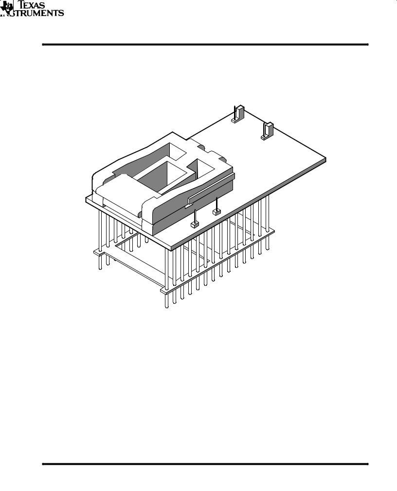
The TMS320E25 includes a 4K × 16-bit EPROM, implemented from an industry-standard EPROM cell, to perform prototyping and early field testing and to achieve low-volume production. When used with a 4K-word masked-ROM TMS320C25, the TMS320E25 yields a high-volume, low-cost production as a result of more migration paths for data. An EPROM adapter socket (part # TMDX3270120), shown in Figure 8, is available to provide 68-pin to 28-pin conversion for programming the TMS320E25.
INFORMATION ADVANCE
Figure 8. EPROM Adapter Socket
Key features of the EPROM cell include standard programming and verification. For security against copyright violations, the EPROM cell features an internal protection mechanism to prevent proprietary code from being read. The protection feature can be used to protect reading the EPROM contents. This section describes erasure, fast programming and verification, and EPROM protection and verification.
fast programming and verification
The TMS320E25 EPROM cell is programmed using the same family and device codes as the TMS27C64 8K × 8-bit EPROM. The TMS27C64 EPROM series are ultraviolet-light erasable, electrically programmable read-only memories, fabricated using HVCMOS technology. The TMS27C64 is pin-compatible with existing 28-pin ROMs and EPROMs. The TMS320E25, like the TMS27C64, operates from a single 5-V supply in the read mode; however, a 12.5-V supply is needed for programming. All programming signals are TTL level. For programming outside the system, existing EPROM programmers can be used. Locations may be programmed singly, in blocks, or at random. When programmed in blocks, the data is loaded into the EPROM cell one byte at a time, the high byte first and the low byte second.
58 |
POST OFFICE BOX 1443 • HOUSTON, TEXAS 77001 |
TMS320E25
SPRS010B Ð MAY 1987 Ð REVISED NOVEMBER 1990
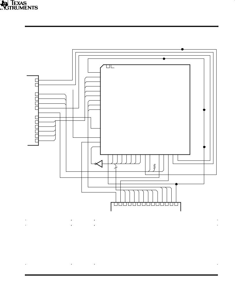
Figure 9 shows the wiring conversion to program the TMS320E25 using the 28-pin pinout of the TMS27C64. The pin nomenclature table provides a description of the TMS27C64 pins. The code to be programmed into the device should be serial mode. The TMS320E25 uses 13 address lines to address the 4K-word memory in byte format.
|
|
|
|
|
|
|
|
|
|
|
|
|
9 |
8 |
|
|
|
|
|
|
|
|
|
|
|
|
|
|
|
|
|
|
|
|
|
|
|
|
|
RS |
|
|
|
|
|
|
|
|
|
|
|
|
|
|
||||
|
|
|
|
|
|
|
|
|
|
|
|
|
|
|
|
|
|
|
|
|
|
|
|
|
|
|
|
|
|
|
|
|
|
|
|
|
|
|
|
|
|
|
|
|
|
|
|
|
|
|
|
|||||||
|
|
|
|
|
|
|
|
|
|
|
|
|
|
|
|
|
|
|
|
|
|
|
|
|
|
|
|
|
|
|
|
|
|
|
|
|
|
|
|
|
|
|
|
|
|
|
|
|
|
|
|
|||||||
|
|
|
|
|
|
|
|
|
|
|
|
|
|
|
|
|
|
|
|
|
|
|
|
|
|
|
|
|
|
|
|
|
|
|
|
|
|
|
|
|
|
|
|
|
|
|
|
|
|
|
|
|
|
|||||
|
|
|
|
|
|
|
|
|
|
|
|
|
|
7 |
|
|
6 |
|
5 |
|
4 |
|
3 |
|
2 |
|
|
1 |
|
68 |
|
67 |
|
66 |
|
65 |
|
64 |
|
63 |
|
62 |
|
61 |
|
|
|
|||||||||||
TMS27C64 |
|
D7 |
|
10 |
|
|
|
|
|
|
|
|
|
|
|
|
|
|
|
|
|
|
|
|
|
|
|
|
|
|
|
|
|
|
|
|
|
|
|
60 |
|
|
||||||||||||||||
|
|
11 |
|
|
|
|
|
|
|
|
|
|
|
|
|
|
|
|
|
|
|
|
|
|
|
|
|
|
|
|
|
|
|
|
|
|
|
59 |
|
|
||||||||||||||||||
28 |
|
VCC |
|
|
|
|
|
|
|
|
|
|
|
|
|
|
|
|
|
|
|
|
|
|
|
|
|
|
|
|
|
|
|
|
|
|
|
|
|
|
|
|||||||||||||||||
|
|
|
|
|
|
|
|
|
|
|
|
|
|
|
|
|
|
|
|
|
|
|
|
|
|
|
|
|
|
|
|
|
|
|
|
|
|
|
||||||||||||||||||||
|
|
D6 |
|
|
|
|
|
|
|
|
|
|
|
|
|
|
|
|
|
|
|
|
|
|
|
|
|
|
|
|
|
|
|
|
|
|
|
|
|
|
||||||||||||||||||
|
|
12 |
|
|
|
|
|
|
|
|
|
|
|
|
|
|
|
|
|
|
|
|
|
|
|
|
|
|
|
|
|
|
|
|
|
|
|
58 |
|
|
||||||||||||||||||
|
|
|
|
|
|
|
|
|
|
|
|
|
|
|
|
|
|
|
|
|
|
|
|
|
|
|
|
|
|
|
|
|
|
|
|
|
|
|
|
|
|
|
|
|
|
|
|
|
|
|
||||||||
27 |
|
PGM |
|
D5 |
|
|
|
|
|
|
|
|
|
|
|
|
|
|
|
|
|
|
|
|
|
|
|
|
|
|
|
|
|
|
|
|
|
|
|
|
|
|
||||||||||||||||
|
|
|
13 |
|
|
|
|
|
|
|
|
|
|
|
|
|
|
|
|
|
|
|
|
|
|
|
|
|
|
|
|
|
|
|
|
|
|
|
57 |
|
|
|||||||||||||||||
|
EPT |
|
|
|
|
|
|
|
|
|
|
|
|
|
|
|
|
|
|
|
|
|
|
|
|
|
|
|
|
|
|
|
|
|
|
|
|
|
|
|
|
|||||||||||||||||
26 |
|
|
D4 |
|
|
|
|
|
|
|
|
|
|
|
|
|
|
|
|
|
|
|
|
|
|
|
|
|
|
|
|
|
|
|
|
|
|
|
|
|
|
|||||||||||||||||
|
|
|
14 |
|
|
|
|
|
|
|
|
|
|
|
|
|
|
|
|
|
|
|
|
|
|
|
|
|
|
|
|
|
|
|
|
|
|
|
56 |
|
|
|||||||||||||||||
|
A8 |
|
|
|
|
|
|
|
|
|
|
|
|
|
|
|
|
|
|
|
|
|
|
|
|
|
|
|
|
|
|
|
|
|
|
|
|
|
|
|
||||||||||||||||||
25 |
|
|
D3 |
|
|
|
|
|
|
|
|
|
|
|
|
|
|
|
|
|
|
|
|
|
|
|
|
|
|
|
|
|
|
|
|
|
|
|
|
|
|
|||||||||||||||||
|
|
|
15 |
|
|
|
|
|
|
|
|
|
|
|
|
|
|
|
|
|
|
|
|
|
|
|
|
|
|
|
|
|
|
|
|
|
|
|
55 |
|
|
|||||||||||||||||
|
A9 |
|
|
|
|
|
|
|
|
|
|
|
|
|
|
|
|
|
|
|
|
|
|
|
|
|
|
|
|
|
|
|
|
|
|
|
|
|
|
|
||||||||||||||||||
24 |
|
|
D2 |
|
|
|
|
|
|
|
|
|
|
|
|
|
|
|
|
|
|
|
|
|
|
|
|
|
|
|
|
|
|
|
|
|
|
|
|
|
|
|||||||||||||||||
|
|
|
16 |
|
|
|
|
|
|
|
|
|
|
|
|
|
|
|
|
|
|
|
|
|
|
|
|
|
|
|
|
|
|
|
|
|
|
|
54 |
|
|
|||||||||||||||||
|
A11 |
|
|
|
|
|
|
|
|
|
|
|
|
|
|
|
|
|
|
|
|
|
|
|
|
|
|
|
|
|
|
|
|
|
|
|
|
|
|
|
||||||||||||||||||
23 |
|
|
D1 |
|
|
|
|
|
|
|
|
|
|
|
|
|
|
|
|
|
|
|
|
|
|
|
|
|
|
|
|
|
|
|
|
|
|
|
|
|
|
|||||||||||||||||
|
|
|
17 |
|
|
|
|
|
|
|
|
|
|
|
|
|
|
|
|
|
|
|
|
|
|
|
|
|
|
|
|
|
|
|
|
|
|
|
53 |
|
|
|||||||||||||||||
|
|
|
|
|
|
|
|
|
|
|
|
|
|
|
|
|
|
|
|
|
|
|
|
|
|
|
|
|
|
|
|
|
|
|
|
|
|
|
|
|
|
|
|
|
|
|
|
|
|
|
||||||||
22 |
|
G |
|
D0 |
|
|
|
|
|
|
|
|
|
|
|
|
|
|
TMS320E25 |
|
|
|
|
|
|
|
|
|
|
|
|
CLKIN |
||||||||||||||||||||||||||
|
|
|
18 |
|
|
|
|
|
|
|
|
|
|
|
|
|
|
|
|
|
|
|
|
|
|
|
|
52 |
|
|||||||||||||||||||||||||||||
21 |
|
A10 |
|
|
|
|
|
|
|
19 |
|
|
|
|
|
|
|
|
|
|
|
|
|
68-Pin (FZ) |
|
|
|
|
|
|
|
|
|
|
|
51 |
|
|
||||||||||||||||||||
|
|
|
|
|
|
|
|
|
|
|
|
|
|
|
|
|
|
|
|
|
|
|
|
|
|
|
|
|
|
|
|
|
|
|||||||||||||||||||||||||
|
|
|
|
|
|
|
|
|
|
|
|
|
|
|
|
|
|
|
|
|
|
|
|
|
|
|
|
|
|
|
|
|
|
|
|
|
|
|
|
|
|
|
|
|
|
|
|
|
|
|
||||||||
20 |
|
E |
|
|
|
|
|
|
|
|
|
|
|
|
|
|
|
|
|
|
|
|
|
|
|
|
|
|
|
|
|
|
|
|
|
|
|
|
|
|
|
|
|
|
|
|
||||||||||||
|
|
|
|
|
|
|
|
|
|
|
|
|
|
|
|
|
|
|
|
|
|
|
|
|
|
|
|
|
|
|
|
|
|
|
|
|
|
|
|
|
|
|
|
|
||||||||||||||
|
|
|
|
|
|
|
|
20 |
|
|
|
|
|
|
|
|
|
|
|
|
|
|
|
|
|
|
|
|
|
|
|
|
|
|
|
|
|
|
|
|
|
|
|
50 |
|
|
||||||||||||
19 |
|
Q8 |
|
|
|
|
|
|
|
|
|
|
|
|
|
|
|
|
|
|
|
|
|
|
|
|
|
|
|
|
|
|
|
|
|
|
|
|
|
|
|
|
|
|
|
|
||||||||||||
|
|
|
|
|
|
|
|
21 |
|
|
|
|
|
|
|
|
|
|
|
|
|
|
|
|
|
|
|
|
|
|
|
|
|
|
|
|
|
|
|
|
|
|
|
49 |
|
|
||||||||||||
18 |
|
Q7 |
|
E |
|
22 |
|
|
|
|
|
|
|
|
|
|
|
|
|
|
|
|
|
|
|
|
|
|
|
|
|
|
|
|
|
|
|
|
|
|
|
48 |
|
|
||||||||||||||
|
Q6 |
|
|
|
|
|
|
|
|
|
|
|
|
|
|
|
|
|
|
|
|
|
|
|
|
|
|
|
|
|
|
|
|
|
|
|
|
|
|
|
||||||||||||||||||
17 |
|
|
|
|
|
|
|
|
|
|
|
|
|
|
|
|
|
|
|
|
|
|
|
|
|
|
|
|
|
|
|
|
|
|
|
|
|
|
|
|
|
|
|
|
|
|||||||||||||
|
|
|
|
|
|
|
|
23 |
|
|
|
|
|
|
|
|
|
|
|
|
|
|
|
|
|
|
|
|
|
|
|
|
|
|
|
|
|
|
|
|
|
|
|
47 |
|
|
||||||||||||
16 |
|
Q5 |
EPT |
|
|
|
|
|
|
|
|
|
|
|
|
|
|
|
|
|
|
|
|
|
|
|
|
|
|
|
|
|
|
|
|
|
|
|
|
|
|
|
|
46 |
|
|
||||||||||||
|
|
Q4 |
|
|
|
|
|
|
|
24 |
|
|
|
|
|
|
|
|
|
|
|
|
|
|
|
|
|
|
|
|
|
|
|
|
|
|
|
|
|
|
|
|
|
|
|
|
|
|||||||||||
15 |
|
VPP |
|
|
|
|
|
|
|
|
|
|
|
|
|
|
|
|
|
|
|
|
|
|
|
|
|
|
|
|
|
|
|
|
|
|
|
|
|
|
|
45 |
|
|
||||||||||||||
|
|
|
|
|
|
|
|
|
|
|
|
|
|
|
|
|
|
|
|
|
|
|
|
|
|
|
|
|
|
|
|
|
|
|
|
|
|
|
|
|
||||||||||||||||||
|
|
|
|
|
|
|
|
A0 |
|
|
|
25 |
|
|
|
|
|
|
|
|
|
|
|
|
|
|
|
|
|
|
|
|
|
|
|
|
|
|
|
|
|
|
|
|
|
|
|
|
|
|||||||||
|
|
|
|
|
|
|
|
|
|
|
|
|
|
|
|
|
|
|
|
|
|
|
|
|
|
|
|
|
|
|
|
|
|
|
|
|
|
|
|
|
|
|
|
|
|
|
44 |
|
|
|||||||||
|
|
|
|
|
|
|
|
|
|
|
|
|
|
26 |
|
|
|
|
|
|
|
|
|
|
|
|
|
|
|
|
|
|
|
|
|
|
|
|
|
|
|
|
|
|
|
|
|
|
|
|
|
|||||||
|
|
|
|
|
|
|
|
|
|
|
|
|
|
|
|
|
|
|
|
|
|
|
|
|
|
|
|
|
|
|
|
|
|
|
|
|
|
|
|
|
|
|
|
|
|
|
|
|
|
|
||||||||
|
|
|
|
|
|
|
|
|
|
|
|
|
|
27 |
28 29 30 31 32 33 34 35 36 37 38 39 40 41 42 43 |
|
|
|||||||||||||||||||||||||||||||||||||||||
|
|
|
|
|
|
|
|
|
|
|
|
|
|
|
|
|
|
|
|
|
|
|
|
|
|
|
|
|
|
|
|
|
|
|
|
|
|
|
|
|
|
|
|
|
|
|
|
|
|
|
|
|
|
|
|
|
|
|
|
|
|
|
|
|
|
|
|
|
|
|
|
|
SS |
A1 |
A2 |
|
A3 |
A4 |
A5 |
A6 |
|
|
CC |
|
|
|
|
A9 |
|
A10 |
A11 |
A12 |
|
|
|
G |
|
|
|||||||||||||||||||
|
|
|
|
|
|
|
|
|
|
|
|
|
|
|
|
|
|
|
|
|
|
|
|
|
|
|
||||||||||||||||||||||||||||||||
|
|
|
|
|
|
|
|
|
|
|
|
|
|
|
|
|
|
|
|
|
|
|
|
|
|
|
||||||||||||||||||||||||||||||||
|
|
|
|
|
|
|
|
|
|
|
|
|
|
V |
|
A7 V |
|
|
A8 K |
|
|
PGM |
|
|
||||||||||||||||||||||||||||||||||
|
|
|
|
|
|
|
|
|
|
|
|
|
|
|
|
|
|
|
|
|
|
|
|
|
|
|
|
|
|
|
|
|
|
|
|
|
|
|
|
|
|
|
|
|
|
|
|
|
|
|
|
|
|
|
||||
|
|
|
|
|
|
|
|
|
|
|
|
|
|
|
|
|
|
|
|
8 |
|
|
|
|
|
|
|
|
|
|
|
|
|
3.9 |
|
|
|
|
|
|
|
|
|
|
|
|
|
|
|
|
|
|
|
|
||||
|
|
|
|
|
|
|
|
|
|
|
|
|
|
|
|
|
|
|
|
|
|
|
|
|
|
|
|
|
|
|
|
|
|
|
|
|
|
|
|
|
|
|
|
|
|
|
|
|
|
|
|
|
|
|
|
|
||
|
|
|
|
|
|
|
|
|
|
|
|
|
|
|
|
|
|
|
|
|
|
|
|
|
|
|
|
|
|
|
|
|
|
|
|
|
|
|
|
|
|
|
|
|
|
|
|
|
|
|
|
|
|
|
|
|
|
|
|
|
|
|
V |
A12 |
A7 |
A6 |
A5 |
A4 |
A3 |
A2 |
A1 |
A0 |
Q1 |
Q2 |
Q3 |
GND |
|
|
|
TMS27C64 |
PP |
|
|
|
|
|
|
|
|
|
|
|
|
|
|
|
|
1 |
2 |
3 |
4 |
5 |
6 |
7 |
8 |
9 |
10 |
11 |
12 |
13 |
14 |
|
|
|
Pin Nomenclature (TMS320E25) |
|
|
|
|
|
||||||||||
|
|
|
|
|
|
|
|
|
|
|
|
|
|
||||
SIGNALS |
I/O |
|
|
|
|
|
|
|
|
|
DEFINITION |
|
|
||||
|
|
|
|
|
|
|
|
||||||||||
A12 (MSB) - A0 (LSB) |
I |
|
On-chip EPROM programming address lines |
|
|
|
|
||||||||||
CLIN |
I |
|
Clock oscillator input |
|
|
|
|
|
|
|
|
|
|
|
|||
E |
I |
|
EPROM chip select |
|
|
|
|
|
|
|
|
|
|
|
|||
EPT |
I |
|
EPROM test mode select |
|
|
|
|
|
|
|
|
|
|
||||
G |
I |
|
EPROM read/verify select |
|
|
|
|
|
|
|
|
|
|||||
GND |
I |
|
Ground |
|
|
|
|
|
|
|
|
|
|
|
|
|
|
PGM |
I |
|
EPROM write/program select |
|
|
|
|
|
|
|
|
||||||
Q8 (MSB) - Q1 (LSB) |
I/O |
|
Data lines for byte-wide programming of on-chip 8K bytes of EPROM |
||||||||||||||
RS |
I |
|
Reset for initializing the device |
|
|
|
|
|
|
|
|
||||||
VCC |
I |
|
5-V power supply |
|
|
|
|
|
|
|
|
|
|
|
|
||
VPP |
I |
|
12.5-V power supply |
|
|
|
|
|
|
|
|
|
|
|
|||
Figure 9. TMS320E25 EPROM Conversion to TMS27C64 EPROM Pinout
ADVANCE INFORMATION
POST OFFICE BOX 1443 • HOUSTON, TEXAS 77001 |
59 |

TMS320E25
INFORMATION ADVANCE
SPRS010B Ð MAY 1987 Ð REVISED NOVEMBER 1990
Table 5 shows the programming levels required for programming, verifying and reading the EPROM cell. The paragraphs following the table describe the function of each programming level.
Table 5. TMS320E25 Programming Mode Levels
SIGNAL |
TMS320E25 |
TMS27C64 |
PROGRAM |
PROGRAM |
PROGRAM |
|
READ |
OUTPUT |
||||||||||||
NAME ² |
PIN |
PIN |
VERIFY |
INHIBIT |
|
DISABLE |
||||||||||||||
|
|
|
|
|
|
|||||||||||||||
|
|
|
|
|
|
|
|
22 |
20 |
|
VIL |
|
VIL |
VIH |
|
VIL |
VIL |
|||
|
|
|
E |
|
|
|
|
|
|
|
||||||||||
|
|
|
|
|
|
|
|
42 |
22 |
|
VIH |
|
|
|
X |
|
|
|
VIH |
|
|
|
|
G |
|
|
|
|
|
PULSE |
|
|
PULSE |
|
|||||||
|
|
|
|
|
|
|
|
41 |
27 |
|
|
|
|
VIH |
X |
|
VIH |
VIH |
||
|
PGM |
|
|
PULSE |
|
|
|
|||||||||||||
|
VPP |
25 |
1 |
|
VPP |
|
VPP |
VPP |
|
VCC |
VCC |
|||||||||
|
VCC |
61,35 |
28 |
VCC + 1 |
VCC + 1 |
VCC + 1 |
|
VCC |
VCC |
|||||||||||
|
VSS |
27,44,10 |
14 |
|
VSS |
|
VSS |
VSS |
|
VSS |
VSS |
|||||||||
CLKIN |
52 |
14 |
|
VSS |
|
VSS |
VSS |
|
VSS |
VSS |
||||||||||
|
|
|
|
|
|
|
|
65 |
14 |
|
VSS |
|
VSS |
VSS |
|
VSS |
VSS |
|||
|
|
RS |
|
|
|
|
||||||||||||||
|
EPT |
24 |
26 |
|
VSS |
|
VSS |
VSS |
|
VSS |
VSS |
|||||||||
Q1-Q8 |
18-11 |
11-13,15-19 |
|
DIN |
|
QOUT |
HI-Z |
|
QOUT |
HI-Z |
||||||||||
A12-A10 |
40-38 |
2,23,21, |
|
ADDR |
|
ADDR |
X |
|
ADDR |
X |
||||||||||
|
|
|
|
|
|
|
|
|
|
|
||||||||||
A9-A7 |
37,36,34 |
24,25,3 |
|
ADDR |
|
ADDR |
X |
|
ADDR |
X |
||||||||||
|
|
|
|
|
|
|
|
|
|
|
|
|
||||||||
|
|
A6 |
33 |
4 |
|
ADDR |
|
ADDR |
X |
|
ADDR |
X |
||||||||
|
|
|
|
|
|
|
|
|
|
|
|
|
||||||||
|
|
A5 |
32 |
5 |
|
ADDR |
|
ADDR |
X |
|
ADDR |
X |
||||||||
|
|
|
|
|
|
|
|
|
|
|
|
|
||||||||
|
|
A4 |
31 |
3 |
|
ADDR |
|
ADDR |
X |
|
ADDR |
X |
||||||||
|
|
|
|
|
|
|
|
|
|
|
||||||||||
A3-A0 |
30-28,26 |
7-10 |
|
ADDR |
|
ADDR |
X |
|
ADDR |
X |
||||||||||
² In accordance with TMS27C64.
LEGEND;
VIH = TTL high level; VIL = TTL low level; ADDR = byte address bit
VPP = 12.5 V ± 0.5 V; VCC = 5 ± 0.25 V; X = don't care
PULSE = low-going TTL level pulse; DIN = byte to be programmed at ADDR
QOUT = byte stored at ADDR; RBIT = ROM protect bit.
erasure
Before programming, the device is erased by exposing the chip through the transparent lid to high-intensity ultraviolet light (wavelength 2537 Å). The recommended minimum exposure dose (UV-intensity × exposure-time) is 15 W•s/cm2. A typical 12 mW/cm2, filterless UV lamp will erase the device in 21 minutes. The lamp should be located approximately 2.5 cm above the chip during erasure. After erasure, all bits are in the high state. Note that normal ambient light contains the correct wavelength for erasure. Therefore, when using the TMS320E25, the window should be covered with an opaque label.
fast programming
After erasure (all memory bits in the cell are logic one), logic zeroes are programmed into the desired locations. The fast programming algorithm, shown in Figure 10, is normally used to program the entire EPROM contents, although individual locations may be programmed separately. A programmed logic zero can be erased only by ultraviolet light. Data is presented in parallel (eight bits) on pins Q8-Q1. Once addresses and data are stable, PGM is pulsed. The programming mode is achieved when VPP = 12.5 V, PGM = VIL, VCC = 6 V, G = VIH, and E = VIL More than one TMS320E25 can be programmed when the devices are connected in parallel. Locations can be programmed in any order.
Programming uses two types of programming pulses: prime and final. The length of the prime pulse is 1 ms. After each prime pulse, the byte being programmed is verified. If correct data is read, the final programming pulse is applied; if correct data is not read, an additional 1-ms prime pulse is applied up to a maximum of 15 times. The final programming pulse is 4 ms times the number of prime programming pulses applied. This sequence of programming and verification is performed at VCC = 6 V, and VPP = 12.5 V. When the full fast programming routine is complete, all bits are verified with VCC = VPP = 5 V.
60 |
POST OFFICE BOX 1443 • HOUSTON, TEXAS 77001 |