

TMS320C25, TMS320E25
SPRS010B Ð MAY 1987 Ð REVISED NOVEMBER 1990
RS, INT, BIO, AND XF TIMING
switching characteristics over recommended operating conditions (see Note 3 and 8)
|
|
|
PARAMETER |
MIN |
TYP |
MAX |
UNIT |
||
|
|
|
|
|
|
|
|
|
|
td(RS) |
CLKOUT1 low to reset state entered |
|
|
22² |
ns |
||||
td(IACK) |
CLKOUT1 to |
|
valid |
± 6 |
0 |
12 |
ns |
||
IACK |
|||||||||
|
|
|
|
|
|
||||
td(XF) |
XF valid before falling edge of |
STRB |
|
Q ± 15 |
|
|
ns |
||
NOTES: 3. Q = 1/4tc(C).
8.RS, INT, and BIO are asynchronous inputs and can occur at any time during a clock cycle. However, if the specified setup time is met, the exact sequence shown in the timing diagrams will occur.
timing requirements over recommended operating conditions (see Note 3 and 8)
|
|
|
|
|
|
|
|
MIN |
NOM MAX |
UNIT |
|
|
|
|
|
|
|
|
|
|
|
tsu(IN) |
|
|
|
|
|
|
|
32 |
|
ns |
INT/BIO/RS setup before CLKOUT1 high |
|
|||||||||
th(IN) |
|
|
|
|
|
|
|
0 |
|
ns |
INT/BIO/RS hold after CLKOUT1 high |
|
|||||||||
t |
|
|
|
|
|
|
8² |
ns |
||
INT/BIO fall time |
|
|||||||||
f(IN) |
|
|
|
|
|
|
|
|
|
|
tw(IN) |
|
|
|
|
|
|
|
tc(C) |
|
ns |
INT/BIO low pulse duration |
|
|||||||||
tw(RS) |
|
3tc(C) |
|
ns |
||||||
RS |
low pulse duration |
|
||||||||
² Value derived from characterization data and not tested. NOTES: 3. Q = 1/4tc(C).
8.RS, INT, and BIO are asynchronous inputs and can occur at any time during a clock cycle. However, if the specified setup time is met, the exact sequence shown in the timing diagrams will occur.
HOLD TIMING
switching characteristics over recommended operating conditions (see Note 3)
|
|
|
|
|
|
|
|
|
|
|
|
PARAMETER |
MIN |
TYP MAX |
UNIT |
||||||
|
|
|
|
|
|
|
|
|
|
|
|
|
|
|
|
|
|
|
|
|
|
td(C1L-AL) |
|
|
|
low after CLKOUT1 low |
0 |
10 |
ns |
||||||||||||||
|
HOLDA |
||||||||||||||||||||
tdis(AL-A) |
|
|
|
|
|
|
|
|
|
|
|
|
|
|
|
|
|
|
0² |
ns |
|
|
HOLDA |
low to address three-state |
|
||||||||||||||||||
tdis(C1L-A) |
|
Address three-state after CLKOUT1 low |
|
|
mode, see Note 9) |
|
20² |
ns |
|||||||||||||
|
(HOLD |
|
|||||||||||||||||||
td(HH-AH) |
|
|
high to |
|
|
|
high |
|
25 |
ns |
|||||||||||
|
HOLD |
HOLDA |
|
||||||||||||||||||
ten(A-C1L) |
|
Address driven before CLKOUT1 low |
|
|
mode, see Note 9) |
|
8² |
ns |
|||||||||||||
|
(HOLD |
|
|||||||||||||||||||
² Value derived from characterization data and not tested. |
|
|
|
||||||||||||||||||
NOTES: 3. |
Q = 1/4tc(C). |
|
|
|
|
|
|
|
|
|
|
|
|||||||||
9. A15-A0, PS, |
DS, |
|
IS, |
|
STRB, |
and R/W |
timings are all included in timings referenced as ªaddress.º |
|
|
||||||||||||
timing requirements over recommended operating conditions (see Note 3)
|
|
|
MIN NOM |
MAX |
UNIT |
|
|
|
|
||
td(C2H-H) |
|
valid after CLKOUT2 high |
|
Q ± 24 |
ns |
HOLD |
|
||||
NOTE 3: Q = 1/4tc(C).
ADVANCE INFORMATION
POST OFFICE BOX 1443 • HOUSTON, TEXAS 77001 |
31 |
TMS320C25, TMS320E25
INFORMATION ADVANCE
SPRS010B Ð MAY 1987 Ð REVISED NOVEMBER 1990
SERIAL PORT TIMING
switching characteristics over recommended operating conditions (see Note 3)
|
PARAMETER |
MIN |
TYP MAX |
UNIT |
|
|
|
|
|
td(CH-DX) |
DX valid after CLKX rising edge (see Note 10) |
|
75 |
ns |
td(FL-DX) |
DX valid after FSX falling edge (TXM = 0, see Note 10) |
|
40 |
ns |
td(CH-FS) |
FSX valid after CLKX rising edge (TXM = 1) |
|
40 |
ns |
NOTES: 3. |
Q = 1/4tc(C). |
|
|
|
10. |
The last occurrence of FSX falling and CLKX rising. |
|
|
|
timing requirements over recommended operating conditions (see Note 3)
|
|
MIN |
NOM MAX |
UNIT |
|
|
|
|
|
tc(SCK) |
Serial port clock (CLKX/CLKR) cycle time² |
200 |
|
ns |
tf(SCK) |
Serial port clock (CLKX/CLKR) fall time |
|
25³ |
ns |
t |
Serial port clock (CLKX/CLKR) rise time |
|
25³ |
ns |
r(SCK) |
|
|
|
|
tw(SCK) |
Serial port clock (CLKX/CLKR) low pulse duration (see Note 11) |
80 |
|
ns |
tw(SCK) |
Serial port clock (CLKX/CLKR) high pulse duration (see Note 11) |
80 |
|
ns |
tsu(FS) |
FSX/FSR setup time before CLKX/CLKR falling edge (TXM = 0) |
18 |
|
ns |
th(FS) |
FSX/FSR hold time after CLKX/CLKR falling edge (TXM = 0) |
20 |
|
ns |
tsu(DR) |
DR setup time before CLKR falling edge |
10 |
|
ns |
th(DR) |
DR hold time after CLKR falling edge |
20 |
|
ns |
² The serial port was tested at a minimum frequency of 1.25 MHz. However, the serial port was fully static but will properly function down
to fsx = 0 Hz.
³ Value derived from characterization data and not tested.
NOTES: 3. Q = 1/4tc(C).
11. The duty cycle of the serial port clock must be within 40-60%.
32 |
POST OFFICE BOX 1443 • HOUSTON, TEXAS 77001 |
TMS320E25
SPRS010B Ð MAY 1987 Ð REVISED NOVEMBER 1990
EPROM PROGRAMMING
absolute maximum ratings over specified temperature range (unless otherwise noted)²
Supply voltage range, VPP³ . . . . . . . . . . . . . . . . . . . . . . . . . . . . . . . . . . . . . . . . . . . . . . . . . . . . . . . |
± 0.6 V to 15 V |
Input voltage range on pins 24 and 25 . . . . . . . . . . . . . . . . . . . . . . . . . . . . . . . . . . . . . . . . . . . . . . |
± 0.3 V to 15 V |
² Stresses beyond those listed under ªAbsolute Maximum Ratingsº may cause permanent damage to the device. This is a stress ratingonly, and functional operation of the device at these or any other conditions beyond those indicated in the ªRecommended Operating Conditionsº section of this specification is not implied. Exposure to absolute-maximum-rated conditions for extended periods may affect device reliability.
³ All voltage values are with respect to GND.
recommended operating conditions
|
|
MIN |
NOM |
MAX |
UNIT |
|
|
|
|
|
|
VCC |
Programming mode supply voltage (see Note 13) |
|
6 |
|
V |
VCC |
Read mode supply voltage |
4.75 |
5 |
5.25 |
V |
VPP |
Programming mode supply voltage |
12 |
12.5 |
13 |
V |
VPP |
Read mode supply voltage (see Note 12) |
|
VCC |
|
V |
NOTES: 12. VPP can be connected to VCC directly (except in the program mode). VCC supply current in this case would be ICC + IPP. During programming, VPP must be maintained at 12.5 V (± 0.25 V).
13. VCC must be applied before or at the same time as VPP and removed after or at the same time as VPP. This device must not be inserted into or removed from the board when VPP or VCC is applied.
electrical characteristics over specified temperature range (unless otherwise noted)
|
PARAMETER |
TEST CONDITIONS |
MIN TYP§ |
MAX |
UNIT |
IPP1 |
VPP supply current |
VPP = VCC = 5.25 V |
|
100 |
A |
IPP2 |
VPP supply current (during program pulse) |
VPP = 13 V |
30 |
50 |
mA |
§ All typical values for ICC are at VCC = 5 V, TA = 25°C.
recommended timing requirements for programming, TA = 25°C, VCC = 6 V, VPP = 12.5 V
(see Notes 14 and 15)
|
|
|
|
|
|
|
|
MIN |
NOM |
MAX |
UNIT |
|
|
|
|
|
|
|
|
|
|
|
|
tw(IPGM) |
Initial program pulse duration |
0.95 |
1 |
1.05 |
ms |
||||||
tw(FPGM) |
Final pulse duration |
2.85 |
|
78.75 |
ms |
||||||
tsu(A) |
Address setup time |
2 |
|
|
s |
||||||
tsu(E) |
|
|
setup time |
2 |
|
|
s |
||||
E |
|
|
|
||||||||
tsu(G) |
|
|
setup time |
2 |
|
|
s |
||||
G |
|
|
|||||||||
tdis(G) |
Output disable time from |
|
|
|
0 |
|
130¶ |
ns |
|||
G |
|
|
|||||||||
|
|
|
|
|
|
||||||
ten(G) |
Output enable time from |
G |
|
|
|
150¶ |
ns |
||||
tsu(D) |
Data setup time |
2 |
|
|
s |
||||||
tsu(VPP) |
VPP setup time |
2 |
|
|
s |
||||||
tsu(VCC) |
VCC setup time |
2 |
|
|
s |
||||||
th(A) |
Address hold time |
0 |
|
|
s |
||||||
th(D) |
Data hold time |
2 |
|
|
s |
||||||
¶ Value derived from characterization data and not tested.
NOTES: 14. For all switching characteristics and timing measurements, input pulse levels are 0.4 V to 2.4 V and VPP = 12.5 V ± 0.5 V during programming.
15. Common test conditions apply for tdis(G) except during programming.
ADVANCE INFORMATION
POST OFFICE BOX 1443 • HOUSTON, TEXAS 77001 |
33 |
TMS320C25-50
INFORMATION ADVANCE
SPRS010B Ð MAY 1987 Ð REVISED NOVEMBER 1990
absolute maximum ratings over specified temperature range (unless otherwise noted)²
Supply voltage range, VCC³ . . . . . . . . . . . . . . . . . . . . . . . . . . . . . . . . . . . . . . . . . . . . . . . . . . . . . . . |
. ± 0.3 V to 7 V |
Input voltage range . . . . . . . . . . . . . . . . . . . . . . . . . . . . . . . . . . . . . . . . . . . . . . . . . . . . . . . . . . . . . . |
. ± 0.3 V to 7 V |
Output voltage range . . . . . . . . . . . . . . . . . . . . . . . . . . . . . . . . . . . . . . . . . . . . . . . . . . . . . . . . . . . . . |
. ± 0.3 V to 7 V |
Continuous power dissipation . . . . . . . . . . . . . . . . . . . . . . . . . . . . . . . . . . . . . . . . . . . . . . . . . . . . . |
. . . . . . . . 1.5 W |
Operating free-air temperature range . . . . . . . . . . . . . . . . . . . . . . . . . . . . . . . . . . . . . . . . . . . . . . . |
. . . 0°C to 70°C |
Storage temperature range . . . . . . . . . . . . . . . . . . . . . . . . . . . . . . . . . . . . . . . . . . . . . . . . . . . . . . . |
± 55°C to 150°C |
²Stresses beyond those listed under ªAbsolute Maximum Ratingsº may cause permanent damage to the device. This is a stress ratingonly, and functional operation of the device at these or any other conditions beyond those indicated in the ªRecommended Operating Conditionsº section of this specification is not implied. Exposure to absolute-maximum-rated conditions for extended periods may affect device reliability.
³ All voltage values are with respect to VSS.
recommended operating conditions
|
|
|
|
|
|
|
|
|
MIN |
NOM |
MAX |
UNIT |
|
|
|
|
|
|
|
|
|
|
|
|
|
VCC |
Supply voltage |
|
|
|
|
|
|
|
4.75 |
5 |
5.25 |
V |
VSS |
Supply voltage |
|
|
|
|
|
|
|
|
0 |
|
V |
|
|
|
INT0 |
- |
INT2 |
|
2.5 |
|
|
V |
||
|
|
|
|
|
|
|
|
|
|
|||
VIH |
High-level input voltage |
|
CLKIN, CLKX, CLKR |
3.5 |
|
|
V |
|||||
|
|
Other inputs |
2.35 |
|
|
V |
||||||
|
|
|
|
|
|
|
|
|
||||
|
|
|
|
|
|
|
0.8 |
V |
||||
|
|
MP/MC |
|
|
|
|||||||
|
|
|
|
|
|
|
|
|||||
VIL |
Low-level input voltage |
|
CLKIN |
|
|
0.8 |
V |
|||||
|
|
Other inputs |
|
|
0.8 |
V |
||||||
|
|
|
|
|
|
|
|
|
|
|
|
|
IOH |
High-level output current |
|
|
|
|
|
|
|
|
|
300 |
A |
IOL |
Low-level output current |
|
|
|
|
|
|
|
|
|
2 |
mA |
TA |
Operating free-air temperature |
|
|
|
|
|
|
|
0 |
|
70 |
°C |
electrical characteristics over specified free-air temperature range (unless otherwise noted)
|
PARAMETER |
|
|
|
TEST CONDITIONS |
MIN TYP§ |
MAX |
UNIT |
|
VOH |
High-level output voltage |
VCC = MIN, IOH = MAX |
2.4 |
|
V |
||||
VOL |
Low-level output voltage |
VCC = MIN, IOL = MAX |
|
0.6 |
V |
||||
IZ |
High-impedance current |
VCC = MAX |
± 20 |
20 |
A |
||||
II |
Input current |
|
|
|
VI = VSS to VCC |
± 10 |
10 |
A |
|
|
|
|
Normal |
TA = 0°C, VCC = MAX, fx = MAX |
110 |
185 |
|
||
ICC |
Supply current |
|
|
|
|
|
|
mA |
|
|
|
|
|
|
|
||||
|
Idle, HOLD |
50 |
100 |
||||||
|
|
||||||||
CI |
Input capacitance |
|
|
|
|
15 |
|
pF |
|
CO |
Output capacitance |
|
|
|
|
15 |
|
pF |
|
§ All typical values are at VCC = 5 V, TA = 25°C.
34 |
POST OFFICE BOX 1443 • HOUSTON, TEXAS 77001 |
TMS320C25-50
SPRS010B Ð MAY 1987 Ð REVISED NOVEMBER 1990
CLOCK CHARACTERISTICS AND TIMING
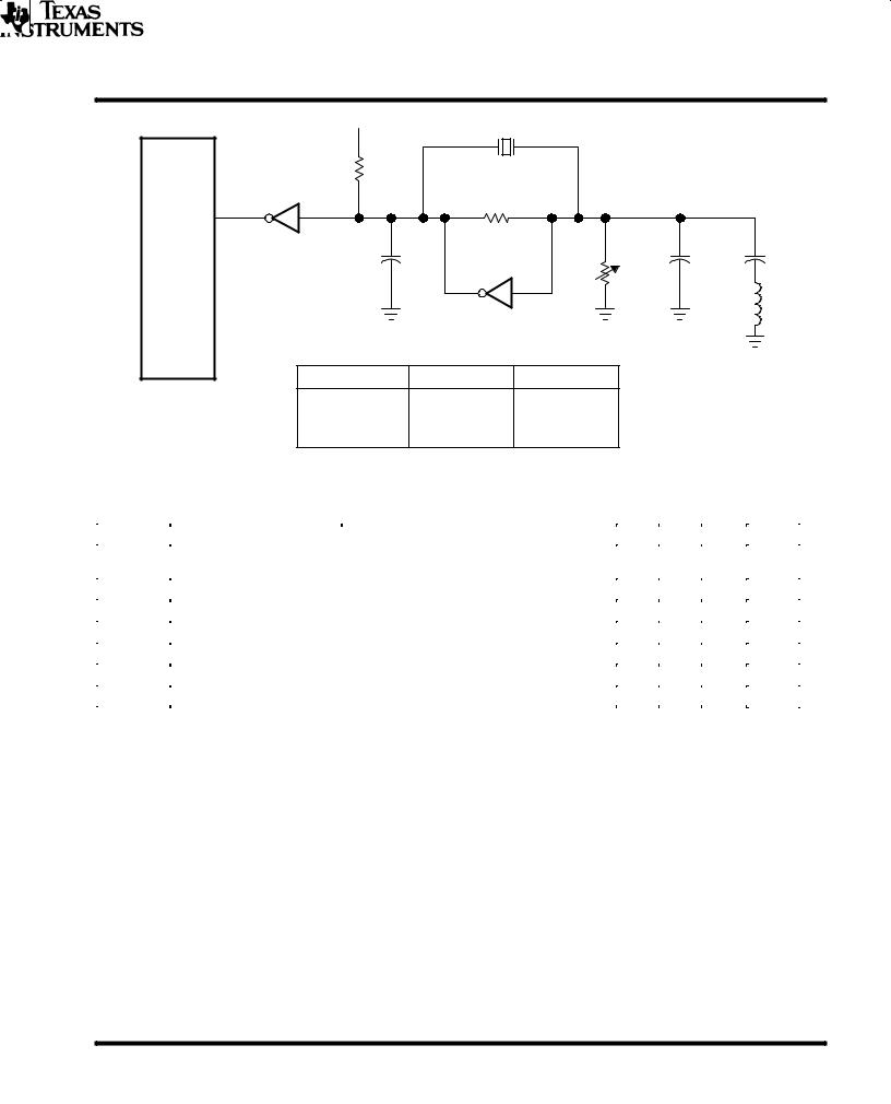
The TMS320C25-50 can use either its internal oscillator or an external frequency source for a clock.
internal clock option
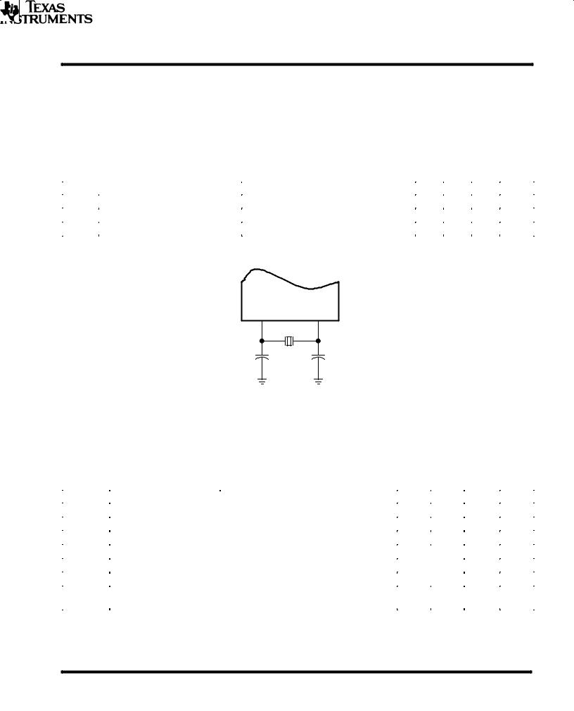
The internal oscillator is enabled by connecting a crystal across X1 and X2, CLKIN. The frequency of CLKOUT1 is one-fourth the crystal fundamental frequency. The crystal should be in either fundamental or overtone mode, and parallel resonant, with an effective series resistance of 30 Ω, a power dissipation of 1 mW, and be specified at a load capacitance of 20 pF. Note that overtone crystals require an additional tuned LC circuit.
|
PARAMETER |
TEST CONDITIONS |
MIN TYP² |
MAX |
UNIT |
fx |
Input clock frequency |
TA = 0°C to 70°C |
6.7 |
51.2 |
MHz |
fsx |
Serial port frequency |
TA = 0°C to 70°C |
0 |
6.4 |
MHz |
C1, C2 |
|
TA = 0°C to 70°C |
10 |
|
pF |
²The serial port was tested at a minimum frequency of 1.25 MHz. However, the serial port was fully static but will properly function down to fsx = 0 Hz.
X1 X2/CLKIN
Crystal
C1 |
C2 |
Figure 6. Internal Clock Option
external clock option
An external frequency source can be used by injecting the frequency directly into X2/CLK, with X1 left unconnected. The external frequency injected must conform to specifications listed in the following table.
switching characteristics over recommended operating conditions (see Note 3)
|
|
|
|
|
|
|
|
MIN |
NOM |
MAX |
UNIT |
|
|
|
|
|
|
|
|
|
|
|
|
tc(C) |
CLKOUT1, CLKOUT2 cycle time |
78.13 |
|
597 |
ns |
||||||
td(CIH-C) |
CLKIN high to CLKOUT1, CLKOUT2, |
|
high, low |
12 |
|
27 |
ns |
||||
STRB |
|
||||||||||
tf(C) |
CLKOUT1, CLKOUT2, |
|
|
fall time |
|
|
4 |
ns |
|||
STRB |
|
|
|
||||||||
tr(C) |
CLKOUT1, CLKOUT2, |
|
|
|
rise time |
|
|
4 |
ns |
||
STRB |
|
|
|||||||||
tw(CL) |
CLKOUT1, CLKOUT2, |
|
|
|
low pulse duration |
2Q ± 7 |
|
2Q + 3 |
ns |
||
STRB |
|
||||||||||
tw(CH) |
CLKOUT1, CLKOUT2, |
|
|
|
high pulse duration |
2Q ± 3 |
|
2Q + 7 |
ns |
||
STRB |
|
||||||||||
td(C1-C2) |
CLKOUT1 high to CLKOUT2 low, |
Q ± 6 |
|
Q + 2 |
ns |
||||||
CLKOUT2 high to CLKOUT1 high, etc. |
|
||||||||||
|
|
|
|
|
|||||||
|
|
|
|
|
|
|
|
|
|
|
|
NOTE 3: Q = 1/4 tc(C) |
|
|
|
|
|||||||
ADVANCE INFORMATION
POST OFFICE BOX 1443 • HOUSTON, TEXAS 77001 |
35 |
TMS320C25-50
INFORMATION ADVANCE
SPRS010B Ð MAY 1987 Ð REVISED NOVEMBER 1990
+5 V |
fcrystal |
|
|
TMS320C25 |
|
|
|
10 kΩ |
|
|
|
74HC04 |
4.7 kΩ |
|
|
F11 |
|
|
|
|
|
|
|
CLKIN |
|
|
|
47 pF |
|
C = 20 pF |
0.1 µF |
74AS04 |
|
|
|
|
10 kΩ |
|
|
|
|
|
|
|
|
|
L |
|
fcrystal, (MHz) |
L, (µH) |
|
TMS320C25 |
40.96 |
1.8 |
|
TMS320C25-50 |
51.20 |
1.0 |
|
TMS320E25 |
40.96 |
1.8 |
|
Figure 7. External Clock Option
timing requirements over recommended operating conditions (see Note 3)
|
|
|
|
MIN |
NOM MAX |
UNIT |
|
|
|
|
|
|
|
tc(CI) |
|
CLKIN cycle time |
19.5 |
150 |
ns |
|
|
3 |
|||||
|
|
|
|
|
|
|
|
|
|
|
|
|
|
t |
|
CLKIN fall time |
|
5 ² |
ns |
|
f(CI) |
|
|
|
|
|
|
t |
|
CLKIN rise time |
|
5² |
ns |
|
r(CI) |
|
|
|
|
|
|
tw(CIL) |
|
CLKIN low pulse duration, tc(CI) = 50 ns (see Note 4) |
20 |
|
ns |
|
tw(CIH) |
|
CLKIN high pulse duration, tc(CI) = 50 ns (see Note 4) |
20 |
|
ns |
|
tsu(S) |
|
|
4 |
Q ± 4 |
ns |
|
|
SYNC |
setup time before CLKIN low |
||||
th(S) |
|
|
hold time from CLKIN low |
4 |
|
ns |
|
SYNC |
|
||||
² Value derived from characterization data and not tested. |
|
|
|
|||
NOTES: 3. |
Q = 1/4 tc(C) |
|
|
|
||
4. CLKIN duty cycle [tr(CI) + tw(CIH)]/tc(CI) must be within 40-60%. |
|
|
|
|||
36 |
POST OFFICE BOX 1443 • HOUSTON, TEXAS 77001 |
TMS320C25-50
SPRS010B Ð MAY 1987 Ð REVISED NOVEMBER 1990
MEMORY AND PERIPHERAL INTERFACE TIMING
switching characteristics over recommended operating conditions (see Note 3)
|
|
|
|
|
|
|
|
|
|
|
|
|
|
|
|
PARAMETER |
MIN |
TYP |
MAX |
UNIT |
||||||||||||||
|
|
|
|
|
|
|
|
|
|
|
|
|
|
|
|
|
|
|
|
|
|
|
|
|
|
|
|
|
|
|
|
|
|
|
td(C1-S) |
|
|
|
|
from CLKOUT (if |
|
|
|
|
|
|
|
|
is present) |
Q ± 5 |
|
Q + 3 |
ns |
||||||||||||||||
|
STRB |
|
STRB |
|
|
|||||||||||||||||||||||||||||
|
|
|
|
|
|
|
|
|
|
|
|
|
|
|
|
|
|
|
|
|
|
|
|
|
|
|
|
|
|
|
||||
td(C2-S) |
|
CLKOUT2 to |
STRB |
(if |
STRB |
|
is present) |
± 2 |
|
5 |
ns |
|||||||||||||||||||||||
tsu(A) |
|
Address setup time before |
|
|
|
|
|
|
|
|
low (see Note 5) |
Q ± 11 |
|
|
ns |
|||||||||||||||||||
|
STRB |
|
|
|||||||||||||||||||||||||||||||
|
|
|
|
|
|
|
|
|
|
|
|
|
|
|
|
|
|
|
|
|
|
|
|
|
||||||||||
tn(A) |
|
Address hold time after |
STRB |
high (see Note 5) |
Q ± 4 |
|
|
ns |
||||||||||||||||||||||||||
tw(SL) |
|
|
|
|
low pulse duration (no wait states, see Note 6) |
2Q ± 5 |
|
2Q + 2 |
ns |
|||||||||||||||||||||||||
|
STRB |
|
|
|||||||||||||||||||||||||||||||
t |
|
|
|
|
high pulse duration (between consecutive cycles, see Note 6) |
2Q ± 2 |
|
2Q + 5² |
ns |
|||||||||||||||||||||||||
|
STRB |
|
||||||||||||||||||||||||||||||||
w(SH) |
|
|
|
|
|
|
|
|
|
|
|
|
|
|
|
|
|
|
|
|
|
|
|
|
|
|
|
|
|
|
|
|
|
|
|
|
|
|
|
|
|
|
|
|
|
|
|
|
|
|
|
|
|
|
|
|
|||||||||||||
tsu(D)W |
|
Data write setup time before |
STRB |
high (no wait) |
2Q ± 17 |
|
|
ns |
||||||||||||||||||||||||||
th(D)W |
|
Data write hold time from |
|
|
|
|
|
|
|
|
high |
Q ± 5 |
|
|
ns |
|||||||||||||||||||
|
STRB |
|
|
|||||||||||||||||||||||||||||||
t |
|
Data bus starts being driven after |
|
|
|
low (write) |
0 ² |
|
|
ns |
||||||||||||||||||||||||
|
STRB |
|
|
|||||||||||||||||||||||||||||||
en(D) |
|
|
|
|
|
|
|
|
|
|
|
|
|
|
|
|
|
|
|
|
|
|
|
|
|
|
|
|
|
|
|
|
|
|
t |
|
Data bus high-impedance state after |
|
|
high, (write) |
|
Q |
Q + 15² |
ns |
|||||||||||||||||||||||||
|
STRB |
|
||||||||||||||||||||||||||||||||
dis(D) |
|
|
|
|
|
|
|
|
|
|
|
|
|
|
|
|
|
|
|
|
|
|
|
|
|
|
|
|
|
|
|
|
|
|
td(MSC) |
|
|
|
|
|
|
|
|
|
|
±1 |
|
9 |
ns |
||||||||||||||||||||
|
MSC |
valid from CLKOUT1 |
|
|||||||||||||||||||||||||||||||
² Value derived from characterization data and not tested. |
|
|
|
|
||||||||||||||||||||||||||||||
NOTES: 3. |
Q = 1/4 tc(C) |
|
|
|
|
|
|
|
|
|
|
|
|
|||||||||||||||||||||
5.A15-A0, PS, DS, IS, R/W, and BR timings are all included in timings referenced as ªaddressº.
6.Delay between CLKOUT1, CLKOUT2, and STRB edges track each other, resulting in tw(SL) and tw(SH) being 2Q with no wait states.
timing requirements over recommended operating conditions (see Note 3)
|
|
|
|
|
|
|
|
|
|
|
|
|
|
|
|
|
|
|
|
|
|
MIN |
NOM |
MAX |
UNIT |
|
|
|
|
|
|
|
|
|
|
|
|
|
|
|
|
|
|
|
|
|
|
|
|
|
|
ta(A) |
Read data access time from address time (see Notes 5 and 7) |
|
|
3Q ± 30 |
ns |
||||||||||||||||||||
tsu(D)R |
Data read setup time before |
|
|
|
|
high |
19 |
|
|
ns |
|||||||||||||||
STRB |
|
|
|||||||||||||||||||||||
th(D)R |
Data read hold time from |
|
|
|
|
|
|
high |
0 |
|
|
ns |
|||||||||||||
STRB |
|
|
|||||||||||||||||||||||
|
|
|
|
|
|
|
|
|
|
|
|
|
|
|
|
|
|
|
|
||||||
td(SL-R) |
READY valid after |
STRB |
low (no wait states) |
|
|
Q ± 21 |
ns |
||||||||||||||||||
td(C2H-R) |
READY valid after CLKOUT2 high |
|
|
Q ± 21 |
ns |
||||||||||||||||||||
th(SL-R) |
READY hold time after |
|
|
|
|
|
|
|
low (no wait states) |
Q ± 1 |
|
|
ns |
||||||||||||
STRB |
|
|
|||||||||||||||||||||||
th(C2H-R) |
READY valid after CLKOUT2 high |
Q ± 1 |
|
|
ns |
||||||||||||||||||||
td(M-R) |
READY valid after |
|
|
|
|
|
|
valid |
|
|
2Q ± 24 |
ns |
|||||||||||||
MSC |
|
|
|||||||||||||||||||||||
th(M-R) |
READY hold time after |
|
|
|
|
|
|
valid |
0 |
|
|
ns |
|||||||||||||
MSC |
|
|
|||||||||||||||||||||||
NOTES: 3. |
Q = 1/4 tc(C) |
|
|
|
|
|
|
|
|
|
|
|
|
||||||||||||
5. A15-A0, PS, DS, IS, R/W, and BR timings are all included in timings referenced as ªaddressº. 7. Read data access time is defined as ta(A) = tsu(A) + tw(SL) ± tsu(D)R.
ADVANCE INFORMATION
POST OFFICE BOX 1443 • HOUSTON, TEXAS 77001 |
37 |
TMS320C25-50
INFORMATION ADVANCE
SPRS010B Ð MAY 1987 Ð REVISED NOVEMBER 1990
RS, INT, BIO, AND XF TIMING
switching characteristics over recommended operating conditions (see Notes 3 and 16)
|
|
|
|
|
|
PARAMETER |
MIN |
TYP MAX |
UNIT |
||
|
|
|
|
|
|
|
|
|
|
|
|
t |
CLKOUT1 low to reset state entered |
|
22² |
ns |
|||||||
d(RS) |
|
|
|
|
|
|
|
|
|
|
|
td(IACK) |
CLKOUT1 to |
|
valid |
± 5 |
7 |
ns |
|||||
IACK |
|||||||||||
td(XF) |
XF valid before falling edge of |
|
|
Q ± 8 |
|
ns |
|||||
STRB |
|
|
|||||||||
² Value derived from characterization data and not tested. |
|
|
|
||||||||
NOTES: 3. |
Q = 1/4 tc(C) |
|
|
|
|||||||
16. |
RS, |
|
INT, |
BIO are asynchronous inputs and can occur at any time during a clock cycle. |
|
|
|
||||
timing requirements over recommended operating conditions (see Notes 3 and 16)
|
|
|
|
|
|
|
|
|
|
|
|
MIN NOM |
MAX |
UNIT |
|
|
|
|
|
|
|
|
|
|
|
|
|
|
|
tsu(IN) |
|
|
|
|
|
|
|
|
|
|
setup before CLKOUT1 high |
25 |
|
ns |
|
INT, |
|
BIO, |
|
RS |
|
||||||||
th(IN) |
|
|
|
|
|
|
0 |
|
ns |
|||||
|
INT, |
|
BIO, |
|
RS |
hold after CLKOUT1 high |
|
|||||||
t |
|
|
|
|
|
|
|
8² |
ns |
|||||
|
INT, |
|
BIO |
fall time |
|
|||||||||
f(IN) |
|
|
|
|
|
|
|
|
|
|
|
|
|
|
tw(IN) |
|
|
|
|
|
|
|
|
low pulse duration |
tc(C) |
|
ns |
||
|
INT, |
|
BIO |
|
||||||||||
tw(RS) |
|
|
|
|
low pulse duration |
3tc(C) |
|
ns |
||||||
|
RS |
|
||||||||||||
² Value derived from characterization data and not tested. |
|
|
|
|||||||||||
NOTES: 3. |
Q = 1/4 tc(C) |
|
|
|
||||||||||
16. |
RS |
, |
INT, |
BIO are asynchronous inputs and can occur at any time during a clock cycle. |
|
|
|
|||||||
HOLD TIMING
switching characteristics over recommended operating conditions (see Note 3)
|
|
|
|
|
|
|
|
|
|
|
PARAMETER |
|
MIN |
TYP MAX |
UNIT |
|||||
|
|
|
|
|
|
|
|
|
|
|
|
|
|
|
|
|
|
|
|
|
t |
|
|
|
low after CLKOUT1 low |
|
1 ² |
11 |
ns |
||||||||||||
|
HOLDA |
|
||||||||||||||||||
d(CIL-AL) |
|
|
|
|
|
|
|
|
|
|
|
|
|
|
|
|
|
|
|
|
t |
|
|
|
low to address high-impedance |
|
|
0 ² |
ns |
||||||||||||
|
HOLDA |
|
|
|||||||||||||||||
dis(AL-A) |
|
|
|
|
|
|
|
|
|
|
|
|
|
|
|
|
|
|
|
|
t |
|
Address high-impedance after CLKOUT1 low |
|
mode, see Note 17) |
|
|
20 ² |
ns |
||||||||||||
|
(HOLD |
|
|
|||||||||||||||||
dis(CIL-A) |
|
|
|
|
|
|
|
|
|
|
|
|
|
|
|
|
|
|
|
|
td(HH-AH) |
|
|
|
|
|
|
|
high |
|
|
19 |
ns |
||||||||
|
HOLD |
high to |
HOLDA |
|
|
|||||||||||||||
t |
|
Address driven before CLKOUT1 low |
|
mode, see Note 17) |
|
|
8 ² |
ns |
||||||||||||
|
(HOLD |
|
|
|||||||||||||||||
en(A-CIL) |
|
|
|
|
|
|
|
|
|
|
|
|
|
|
|
|
|
|
|
|
² Value derived from characterization data and not tested. |
|
|
|
|||||||||||||||||
NOTES: 3. |
Q = 1/4 tc(C) |
|
|
|
|
|
|
|
|
|
||||||||||
17. A15-A0, PS, |
DS, |
|
STRB, |
and R/W |
timings are all included in timings referenced as ªaddressº. |
|
|
|
||||||||||||
timing requirements over recommended operating conditions (see Note 3)
|
|
|
MIN |
NOM MAX |
UNIT |
|
|
|
|
||
td(C2H-H) |
|
valid after CLKOUT2 high |
|
Q ± 19 |
ns |
HOLD |
|
||||
NOTE 3: Q = 1/4 tc(C) |
|
|
|||
38 |
POST OFFICE BOX 1443 • HOUSTON, TEXAS 77001 |
TMS320C25-50
SPRS010B Ð MAY 1987 Ð REVISED NOVEMBER 1990
SERIAL PORT TIMING
switching characteristics over recommended operating conditions (see Note 3)
|
PARAMETER |
MIN |
TYP MAX |
UNIT |
|
|
|
|
|
td(CH-DX) |
DX valid after CLKX rising edge (see Note 18) |
|
75 |
ns |
td(FL-DX) |
DX valid after falling edge (TXM = 0, see Note 18) |
|
40 |
ns |
td(CH-FS) |
FSX valid after CLKX raising edge (TXM = 1) |
|
40 |
ns |
NOTES: 3. |
Q = 1/4 tc(C) |
|
|
|
18. |
The last occurrence of FSX falling and CLKX rising. |
|
|
|
timing requirements over recommended operating conditions (see Note 3)
|
|
MIN |
NOM MAX |
UNIT |
|
|
|
|
|
t |
Serial port clock (CLKX/CLKR) cycle time ² |
160 |
|
ns |
c(SCK) |
|
|
|
|
t |
Serial port clock (CLKX/CLKR) fall time |
|
25 ³ |
ns |
f(SCK) |
|
|
|
|
t |
Serial port clock (CLKX/CLKR) rise time |
|
25 ³ |
ns |
r(SCK) |
|
|
|
|
tw(SCK) |
Serial port clock (CLKX/CLKR) low or high pulse duration (see Note 19) |
64 |
|
ns |
tsu(FS) |
FSX or FSR setup time before CLKX, CLKR falling edge (TXM = 0) |
5 |
|
ns |
th(FS) |
FSX or FSR hold time before CLKX, CLKR falling edge (TXM = 0) |
10 |
|
ns |
tsu(DR) |
DR setup time before CLKR falling edge |
5 |
|
ns |
th(DR) |
DR hold time after CLKR falling edge |
10 |
|
ns |
² The serial port was tested at a minimum frequency of 1.25 MHz. However, the serial port was fully static but will properly function down to
fsx = 0 Hz.
³ Value derived from characterization data and not tested.
NOTES: 3. Q = 1/4 tc(C)
19. The cycle of the serial port must be within 40%-60%.
CONTRAST SUMMARY OF ELECTRICAL SPECIFICATIONS
The following table presents electrical parameters which differ between TMS320C25 (40 MHz, 100 ns) and TMS320C25-50 (50 MHz, 80 ns).
clock characteristics and timing
|
PARAMETER |
|
TMS320C25 |
TMS320C25-50 |
UNIT |
||||
|
|
|
|
|
|
|
|||
|
MIN |
TYP |
MAX |
MIN |
TYP |
MAX |
|||
|
|
|
|
||||||
|
|
|
|
|
|
|
|
|
|
tc(SCK) |
|
97.7 |
|
597 |
78.13 |
|
597 |
ns |
|
td(CIH-C) |
|
5 |
|
30 |
12 |
|
27 |
ns |
|
tf(C) |
|
|
|
5 |
|
|
4 |
ns |
|
tr(C) |
|
|
|
5 |
|
|
4 |
ns |
|
tw(CL) |
|
2Q ± 8 |
2Q |
2Q + 8 |
2Q ± 7 |
|
2Q + 3 |
ns |
|
tw(CH) |
|
2Q ± 8 |
2Q |
2Q + 8 |
2Q ± 3 |
|
2Q + 7 |
ns |
|
td(C1-C2) |
|
Q ± 5 |
Q |
Q + 5 |
Q ± 6 |
|
Q + 2 |
ns |
|
tsu(S) |
|
5 |
|
Q ± 5 |
4 |
|
Q ± 4 |
ns |
|
th(S) |
|
8 |
|
|
4 |
|
|
ns |
|
|
|
|
|
|
|
|
|
|
|
|
|
|
|
|
|
|
|
|
|
ADVANCE INFORMATION
POST OFFICE BOX 1443 • HOUSTON, TEXAS 77001 |
39 |
TMS320C25-50
SPRS010B Ð MAY 1987 Ð REVISED NOVEMBER 1990
memory and peripheral interface timing
|
|
|
|
|
|
|
PARAMETER |
|
|
td(C1-S) |
|||||||
|
td(C2-S) |
|||||||
|
tsu(A) |
|||||||
|
th(A) |
|||||||
|
tw(SL) |
|||||||
|
tw(SH) |
|||||||
|
tsu(D)W |
|||||||
|
th(D)W |
|||||||
|
td(MSC) |
|||||||
|
ta(A) |
|||||||
|
tsu(D)R |
|||||||
ADVANCE |
th(D)R |
|||||||
td(SL-R) |
||||||||
|
||||||||
|
td(C2H-R) |
|||||||
|
th(SL-R) |
|||||||
|
th(C2H-R) |
|||||||
|
td(M-R) |
|||||||
|
th(M-R) |
|||||||
|
|
|
|
|
|
|
and XF timing |
|
INFORMATION |
RS, |
INT, |
BIO, |
|||||
|
|
|
|
|
|
PARAMETER |
||
|
|
|
|
|
|
|||
|
|
|
|
|
|
|
||
|
td(IACK) |
|||||||
|
td(XF) |
|||||||
|
tsu(IN) |
|||||||
|
th(IN) |
|||||||
|
|
timing |
||||||
|
HOLD |
|||||||
|
|
|
|
|
|
|
PARAMETER |
|
|
|
|
|
|
|
|
||
|
td(C1L-AL) |
|||||||
|
td(HH-AH) |
|||||||
|
td(C2H-H) |
|||||||
|
serial port timing |
|||||||
|
|
|
|
|
|
|
PARAMETER |
|
|
|
|
|
|
|
|
||
|
td(CH-DX) |
|||||||
|
td(FL-DX) |
|||||||
|
td(CH-FS) |
|||||||
|
tsu(FS) |
|||||||
|
th(FS) |
|||||||
|
tsu(DR) |
|||||||
|
th(DR) |
|||||||
|
TMS320C25 |
|
TMS320C25-50 |
UNIT |
|||
|
|
|
|
|
|
||
MIN |
TYP |
MAX |
MIN |
TYP |
MAX |
||
|
|||||||
Q ± 6 |
Q |
Q + 6 |
Q ± 5 |
|
Q + 3 |
ns |
|
± 6 |
0 |
6 |
± 2 |
|
5 |
ns |
|
Q ± 12 |
|
|
Q ± 11 |
|
|
ns |
|
Q ± 8 |
|
|
Q ± 4 |
|
|
ns |
|
|
2Q |
|
2Q ± 5 |
|
2Q + 2 |
ns |
|
|
2Q |
|
2Q ± 2 |
|
2Q + 5 |
ns |
|
2Q ± 20 |
|
2Q ± 17 |
|
|
ns |
||
Q ± 10 |
Q |
|
Q ± 5 |
|
|
ns |
|
± 12 |
0 |
12 |
±1 |
|
9 |
ns |
|
|
3Q ± 35 |
|
|
3Q ± 30 |
ns |
||
23 |
|
|
19 |
|
|
ns |
|
0 |
|
|
0 |
|
|
ns |
|
|
Q ± 20 |
|
|
Q ± 21 |
ns |
||
|
Q ± 20 |
|
|
Q ± 21 |
ns |
||
Q + 3 |
|
|
Q ± 1 |
|
|
ns |
|
Q + 3 |
|
|
Q ± 1 |
|
|
ns |
|
|
2Q ± 25 |
|
|
2Q ± 24 |
ns |
||
0 |
|
|
0 |
|
|
ns |
|
|
|
|
|
|
|
|
|
|
TMS320C25 |
TMS320C25-50 |
UNIT |
|||
|
|
|
|
|
||
MIN |
TYP |
MAX |
MIN |
TYP MAX |
||
|
||||||
± 6 |
0 |
12 |
± 5 |
7 |
ns |
|
Q ± 15 |
|
Q ± 8 |
|
ns |
||
32 |
|
|
25 |
|
ns |
|
0 |
|
|
0 |
|
ns |
|
|
|
|
|
|
|
|
|
TMS320C25 |
TMS320C25-50 |
|
||
|
|
|
|
UNIT |
|
MIN |
TYP MAX |
MIN |
TYP MAX |
||
|
|||||
0 |
10 |
1 |
11 |
ns |
|
|
25 |
|
19 |
ns |
|
|
Q ± 24 |
|
Q ± 19 |
ns |
|
|
|
|
|
|
|
|
TMS320C25 |
TMS320C25-50 |
|
||
|
|
|
|
UNIT |
|
MIN |
TYP MAX |
MIN |
TYP MAX |
||
|
|||||
|
75 |
|
70 |
ns |
|
|
40 |
|
40 |
ns |
|
|
40 |
|
40 |
ns |
|
18 |
|
5 |
|
ns |
|
20 |
|
10 |
|
ns |
|
10 |
|
5 |
|
ns |
|
20 |
|
10 |
|
ns |
|
|
|
|
|
|
|
40 |
POST OFFICE BOX 1443 • HOUSTON, TEXAS 77001 |