

Broadband Packet Switching Technologies
.pdf238 CROSSPOINT BUFFERED SWITCHES
In case 2, the low-priority load of the third input port is 0.4 and that of other input ports is 0.03, as shown in Table 8.2. The high-priority input load is the same as in case 1. The total input load is 1.2 Ž0.6 q 0.6., which is also overloaded. The low-priority throughput for input ports except for the third input port is 0.03, which is the same as the input load, and the low-priority throughput for the third input port is 0.19, which is larger than 0.03. The low-priority throughput is first equally divided into 0.03, which satisfies the input ports except for the third. Since some bandwidth remains, the residual bandwidth is given to the third input port. Therefore, the low-priority throughput of the third input port is 0.19. This means that the MSDA switch achieves max min fair share for the low-priority class.
REFERENCES
1.H. J. Chao, B.-S. Choe, J.-S Park, and N. Uzun, ‘‘Design and implementation of abacus switch: a scalable multicast ATM switch,’’ IEEE J. Selct. Areas Commun., vol. 15, no. 5, pp. 830 843, 1997.
2.E. Oki and N. Yamanaka, ‘‘Scalable crosspoint buffering ATM switch architecture using distributed arbitration scheme,’’ Proc. IEEE ATM ’97 Workshop, pp. 28 35, 1997.
3.E. Oki and N. Yamanaka, ‘‘A high-speed ATM switch based on scalable distributed arbitration,’’ IEICE Trans. Commun., vol. E80-B, no. 9, pp. 1372 1376, 1997.
4.E. Oki, N. Yamanaka, and M. Nabeshima, ‘‘Scalable-distributed-arbitration ATM switch supporting multiple QoS classes,’’ Proc. IEEE ATM ’99 Workshop, 1999.
5.E. Oki, N. Yamanaka, and M. Nabeshima, ‘‘Performance of scalable-distributed- arbitration ATM switch supporting multiple QoS classes,’’ IEICE Trans. Commun., vol. E83-B, no. 2, pp. 204 213, 2000.
6.H. Tomonaga, N. Matsuoka, Y. Kato, and Y. Watanabe, ‘‘High-speed switching module for a large capacity ATM switching system,’’ Proc. IEEE GLOBECOM ’9 2, pp. 123 127, 1992.
Broadband Packet Switching Technologies: A Practical Guide to ATM Switches and IP Routers
H. Jonathan Chao, Cheuk H. Lam, Eiji Oki
Copyright 2001 John Wiley & Sons, Inc. ISBNs: 0-471-00454-5 ŽHardback.; 0-471-22440-5 ŽElectronic.
CHAPTER 9
THE TANDEM-CROSSPOINT SWITCH
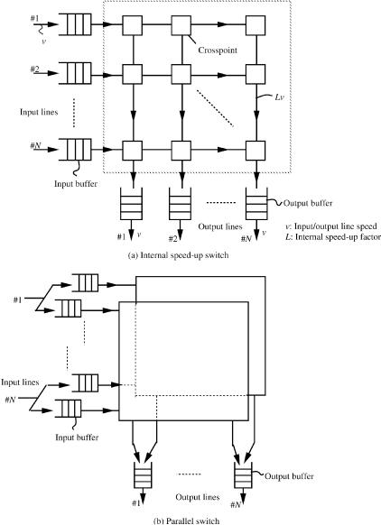
The HOL blocking problem in input-buffered switches can be eliminated by using the parallel-switch technique, where one switch fabric consists of multiple switch planes. The switch fabric operates at the line rate, and thus the arbitration timing is relaxed compared with the internal speedup switch architecture.
However, the parallel-switch architecture suffers from a cell-out-of- sequence problem at output ports. A resequencing circuit needs to be implemented at the output ports to ensure that cells are delivered in order. For example, timestamps can be carried in the cell headers and stored at output buffers.
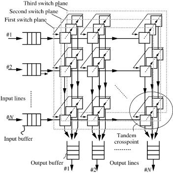
A tandem-crosspoint ŽTDXP. switch w11, 12x developed by NTT has logically multiple crossbar switch planes. These switch planes are connected in tandem at every crosspoint. The TDXP switch achieves a high throughput without increasing the internal speed of switch fabric. It also preserves the cell-sequence order.
The remainder of this chapter is as follows. Section 9.1 briefly reviews basic input and output buffered switch architectures. Section 9.2 presents the TDXP switch architecture. Section 9.3 shows its performance. Throughout this chapter, we assume that the switch size is N N Ž N input ports and N output ports.. Input and output have the same line speed.
9.1 OVERVIEW OF INPUT–OUTPUT-BUFFERED SWITCHES
A switch with a crossbar structure can be easily scaled because of its modularity.
239
240 THE TANDEM-CROSSPOINT SWITCH
One can build a larger switch simply adding more crosspoint switch devices. In addition, the cell transmission delay in the switch is smaller than in Banyan-type switches. This is because it has the smallest number of connecting points between any input output pair.
Variants of crossbar-type switches include the input-buffered switch and the output-buffered switch. The advantage of the former is that the operation
Fig. 9.1 Basic input output-buffered switches.
TDXP STRUCTURE |
241 |
speed of the switch fabric is the same as the input line rate. However, it suffers from the HOL blocking problem. The performance of the inputbuffered switch was analyzed by Karol et al. w5x. They showed that, when the switch size N is infinite, the maximum throughput of the switch is 0.586, assuming that the internal speed of the switch is equal to that of inputr output lines. The limitation of the maximum throughput is due to HOL blocking in the input buffers.
Several problems have to be addressed in order to improve the limited throughput of the input buffering switch w10x. One possible solution to HOL blocking is to increase the internal line speed of the switch as shown in Figure 9.1Ža.. Oie et al. analyzed the performance of the internal speedup switch with input and output buffers when the speedup factor is L Ž1 F L F N . w9x. Yamanaka et al. developed a high-speed switching system that has 160-Gbitrs throughput; the internal line speed was twice that of the inputroutput lines w14, 4, 6x. In the switch reported, the inputroutput speed is 10 Gbitrs, so the internal line speed is 20 Gbitrs. To realize these speeds, the switch adopted ultrahigh-speed Si bipolar devices and special highdensity multichip module ŽMCM. techniques w6, 14x. However, for much larger throughputs this internal speedup crossbar switch architecture is not so cost-effective, given the limitation of current hardware technologies.
Another possible approach to improve the performance of crossbar-type switches is to employ a parallel switch architecture as shown in Figure 9.1Žb. w13, 8x. The parallel switch consists of K identical switch planes. Each switch plane has its own input buffer and shares output buffers with other planes. The parallel switch with K s 2 achieves the maximum throughput of 1.0. This is because the maximum throughput of each switch plane is more than 0.586 for arbitrary switch size N. Using this concept, Balboni et al. developed an industrial 160-Gbitrs cross-connect system w1, 7x. At the input buffers, however, timestamp values must be placed in each cell header. At the output ports, cells are buffered by implementing a maximum-delay equalization mechanism in order to rebuild the cell sequences, which, due to the internal routing algorithm, can not be guaranteed w3x. Thus, this type of parallel switch requires timestamps and also requires cell sequence regeneration at the output buffers. In addition, the hardware resources needed to implement the switch are double those of a single-plane switch. Considering the implementation for much larger switches, rebuilding of the cell sequences at high-speed also makes cost-effective implementation unlikely.
9.2 TDXP STRUCTURE
9.2.1 Basic Architecture
Figure 9.2 shows the structure of the TDXP switch. It has, logically, multiple crossbar switch planes. The number of crossbar switch planes is K in general. The case with K s 3 is shown in Figure 9.2. The larger K is, the better the
242 THE TANDEM-CROSSPOINT SWITCH
Fig. 9.2 Tandem-crosspoint switch structure. Ž 1997 IEEE..
switch performance, is but at the expense of implementation cost. These switch planes are connected in tandem at every crosspoint. That is why this switch is called a TDXP switch. The internal speed in each plane is the same as the inputroutput line speed. In other words, each switch plane can transmit only one cell to each output port within one cell time slot. If more than one cell goes to the same output port on the same switch plane, unsuccessful cells that are not transmitted to the output port are stored in the TDXP. However, the TDXP switch that has multiple switch planes can transmit up to K cells to each output port within one time slot.
9.2.2 Unicasting Operation
The cell transmission algorithm in the TDXP switch for unicasting is first explained.
Step 1 A cell at the head of the input buffer sends a request signal ŽREQ. to the destination TDXP according to the routing bits written in the cell header. Then go to Step 2.
TDXP STRUCTURE |
243 |
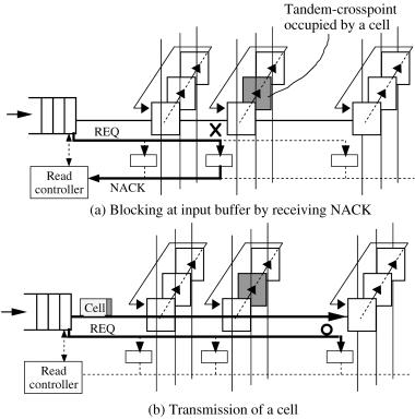
Fig. 9.3 Cell transmission mechanism of TDXP switch. Ž 1997 IEEE..
Step 2 The TDXP that receives an REQ sends a not-acknowledge signal ŽNACK. back to the input buffer if the TDXP is already handling or buffering a cell that cannot be transmitted to the output line because of contention on the output line, as shown in Figure 9.3Ža.. Then go to Step 3.
Step 3 The cell at the head of the input buffer that sent the REQ is sent to the destination crosspoint on the first switch plane if NACK is not received within a certain time, as shown in Figure 9.3Žb.. Then go to Step 4, setting k s 1. Otherwise, the cell is not sent to the crosspoint; at the next cell time, go to Step 1.
Step 4 The k th crosspoint sends a request signal to an arbitration controller asking for transmission to the destination output buffer. ŽWe refer to the crosspoint on the k th plane as the k th crosspoint.. The arbitration control on the k th plane is executed independently of that of the other planes. Ring arbitration is one possible approach. If the request is accepted by the arbitration controller, the cell is transmitted to the output buffer. Then, go to Step 5. Otherwise, the cell is moved to
244 THE TANDEM-CROSSPOINT SWITCH
the k q 1th crosspoint if k is not equal to K , and k is set to k q 1. If k is equal to K , the cell is moved to the first crosspoint and k is set to 1. Then, go back to the beginning of Step 4 after one cell time slot.
Step 5 The cell transmitted from the TDXP is stored in the output buffer. The output buffer can receive more than one cell within one cell time.
It is noted that each TDXP needs only one cell buffer for arbitrary K. This is because, when one cell is stored in a TDXP, the following cell does not go to the same TDXP, due to the back-pressure mechanism.
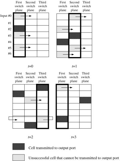
To clarify the cell transmission mechanism, let us consider that K q 1 cells request to be transmitted to the same output port on the first switch plane. First, on the first switch plane, only one cell is transmitted to the output port, and the other K cells go to the second switch plane. At the next cell time slot, only one cell is transmitted to the output port on the second switch plane, and K y 1 cells go to the third plane switch. In the same way, on the K th switch plane, one cell of the remaining two is transmitted to the output port. The unsuccessful cell that cannot be transmitted to the output port goes back to the first switch plane and tries again to be transmitted to the output port, competing with other cells that request to be transmitted on the first switch plane.
Figure 9.4 shows the behavior of the cell transmission mechanism with K s 3, when four cells request to be transmitted to the same output port on the first switch plane at t s 0. In Figure 9.4, the states of only one output port are depicted. At t s 0, the cell at the second input port is transmitted on the first switch plane. Then, the cell at the third input port is transmitted on the second switch plane at t s 1, the cell at the first input port is transmitted on the third switch plane at t s 2, and the cell at the fifth input port is transmitted on the first plane at t s 3.
These procedures are executed in a pipelined manner at every cell time.Therefore, more than one cell can be transmitted to the same output buffer within one cell time slot, even though the internal line speed of each switch plane equals the inputroutput line speed. When K s 3, three cells that come from different input lines can, as the maximum case, be transmitted to the output buffer at the same time slot at t s 2, as shown in Figure 9.4. Thus, the TDXP switch achieves a similar result to the internal speedup switch in eliminating HOL blocking. However, the effect on HOL blocking in the TDXP switch is not exactly same as that of the internal speedup switch. This is because the TDXP switch has one cell buffer at each TDXP and employs a backpressure mechanism in the input buffers, while the internal speedup switch does not have any crosspoint buffers. A detailed discussion is given in Section 9.3, considering the effect of such a backpressure mechanism.
In addition, while a TDXP is handling a cell, the input buffer does not send the head-of-line cell to the same TDXP. The same TDXP never transmits more than one cell within the same cell time slot. Therefore, cell
TDXP STRUCTURE |
245 |
Fig. 9.4 Behavior of cell transmission mechanism Ž K s 3..
sequences are completely guaranteed, and there is no need to rebuild them at the output buffers.
Another advantage of the TDXP switch is that, although it has logically multiple crossbar switch planes, the hardware resources required are much less than for the parallel switch. This is because the parallel switch cannot share the hardware resources, while the TDXP switch can share input buffers, internal input lines, and so on. This is a significant implementation benefit.
246 THE TANDEM-CROSSPOINT SWITCH
9.2.3 Multicasting Operation
Next, we explain the multicasting mechanism in the TDXP switch. Unicast is a subset of multicast. For multicasting, Steps 1 and 3 are modified a little. The remaining procedures, Steps 2, 4, and 5, are the same as above. The modified procedures, Steps 1 and 3 , for multicast are as follows.
Step 1 A cell at the head of the input buffer sends request signals ŽREQ. to all the destination tandem crosspoints according to the routing bits written in the cell header. The routing bits for multicasting are, for example, written using a bit-map scheme. Then go to Step 2.
Step 3 The cell at the head of the input buffer that sent REQ before is sent to all the destination crosspoints on the first switch plane, if no NACK is received from any of the crosspoints polled to the input buffer within a certain time. Then go to Step 4. If even one NACK is received by the input buffer within a certain time, the cell is not sent to any of the destination crosspoints; after the next cell time, go to Step 1 .
9.3 PERFORMANCE OF TDXP SWITCH
The performance of the TDXP switch was evaluated by event-driven computer simulation. The simulation programs were written using the C language. The performance parameters of interest were the maximum throughput, the delay time, and the buffer size required to guarantee a specified cell loss ratio. The maximum throughput is defined as the ratio of the total number of cells transmitted to output ports to the total number of offered input cells. In the estimation of the maximum throughput, all offered input loads are set at 1.0.
Assume that cell arrival at N input ports follows a Bernoulli process. When the input traffic load is , an incoming cell arrives with probability in a cell time, and there is no arrival with probability 1 y . The incoming cells are distributed uniformly to all output ports. The input traffic is assumed to be homogeneous, and it is distributed uniformly to all input ports. Bernoulli traffic is considered. In addition, a simple arbitration mechanism for cell output in the switch Žround-robin arbitration. is established between the crosspoints belonging to the same output port.
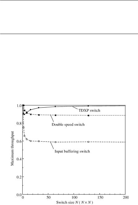
First we present the performance of the TDXP switch for unicasting traffic. Table 9.1 shows how many tandem switch planes K are needed to obtain the maximum throughput in the TDXP switch architecture. To evaluate the maximum throughput, it is assumed that the sizes of the input and output buffers are infinite. We can see that the maximum throughput is almost saturated with K s 2.
We thus conclude that K s 2 is large enough to obtain the maximum throughput. Therefore, in the following performance evaluation of the TDXP
PERFORMANCE OF TDXP SWITCH |
247 |
TABLE 9.1 Maximum Throughput Determined by the Number K of Tandem Switch Planes a
|
|
|
Maximum Throughput |
|
|
K |
N s 8 |
N s 16 |
N s 32 |
N s 64 |
N s 128 |
1 |
0.618 |
0.599 |
0.598 |
0.588 |
0.588 |
2 |
0.922 |
0.948 |
0.970 |
0.983 |
0.990 |
3 |
0.939 |
0.962 |
0.979 |
0.989 |
0.994 |
4 |
0.942 |
0.965 |
0.981 |
0.990 |
0.995 |
aN s switch size.
switch, K is set to 2. In addition, we also show the performance of the conventional internal speedup switch with input and output buffers for reference. The internal speedup factor L is set to 2 for rough equivalency w9x.
The maximum throughput of the TDXP switch increases with switch size N, and is higher than that of the double-speedup switch. Figure 9.5 compares the maximum throughput with those of the internal double-speedup switch Ž L s 2. and the input buffering switch. The maximum throughput of the TDXP switch decreases with small N, say N F 8, and increases with larger N. The reason is as follows. The probability Psuc that two successive cells at
Fig. 9.5 Comparison of maximum throughput. Ž 1997 IEEE..