

The Microcontroller Idea book (Jan Akelson, 1997)
.pdfChapter 2
RAM
RAM (random-access memory) is where programs store information for temporary use. Unlike ROM, the CPU can write to RAM as well as read it. Any information stored in RAM is lost when power is removed from the chip. The 8052 has 256 bytes of RAM. BASIC-52 uses much of this for its own operations, with a few bytes available to users.
I/O Ports
I/O (Input/Output) Ports enable the 8052 to read and write to external memory and other components. The 8052 has four 8-bit I/O ports (Ports 0-3). As the name suggests, the ports can act as inputs (to be read) or outputs (to be written to). Many of the port bits have optional, alternate functions relating to accessing external memory, using the on-chip timer/counters, detecting external interrupts, and handling serial communications. BASIC-52 assigns alternate functions to the remaining port bits. Some of these functions are required by BASIC-52, while others are optional. If you don’t use an alternate function, you can use the bit for any control, monitoring, or other purpose in your application.
Accessing external memory. The largest alternate use of the ports has to do with accessing external memory. Although the 8052 is a single-chip computer, a complete 8052-BASIC system requires additional components. It must have external RAM in addition to the 8052’s internal RAM, and most systems also have EPROM, EEPROM, or battery-backed RAM for permanent storage of BASIC-52 programs.
Accessing this external memory uses all of Ports 0 and 2, plus bits 6 and 7 of Port 3, to hold data, addresses, and control signals for reading and writing to external memory. Data here refers to a byte to be read or written, and may be any type of information, including program code. The address defines the location in memory to be read or written.
During a memory access, Port 0’s eight pins (AD0-AD7) first hold the lower byte of the address, followed by the data to be read or written. This method of carrying both addresses and data on the same signal lines is called a multiplexed address/data bus. It’s a popular arrangement that many devices use, since it requires fewer pins on the chip, compared to giving each data and address line its own pin. Port 2’s eight lines hold the higher byte of the address to be read or written to. These lines make up the high address bus (A8-A15). Together, the 16 address lines can access 64 kilobytes (65,536 bytes) of memory, from 00000000 00000000 to 11111111 11111111 in binary, or 0000h to FFFFh in hexadecimal.
Besides pins to hold the data and addresses, the 8052 must also provide control signals to initiate the read and write operations. Control signals include WR (write), RD (read), PSEN (program store enable), and ALE (address latch enable). Some of the address lines may also function as control signals that help to select a chip during a memory access.
20 |
The Microcontroller Idea Book |

Inside the 8052-BASIC
Code and data memory. To understand the operation of the control signals, you need to know a little about how the 8052 distinguishes between two types of memory: data and code, or program, memory. By using different control signals for each type of memory, the 8052 can access two separate 64K areas of memory, with each addressed from 0000h to FFFFh, and each using the same data and address lines.
The 8052 accesses code memory when it executes an assembly-language program or subroutine. Code memory is read-only; you can’t write to it. The only instructions that access code memory are read operations. Code memory is intended for programs or subroutines that have been previously programmed into ROM or EPROM. The 8052 strobes, or pulses, PSEN when it accesses external code memory. Accesses to internal code memory (the BASIC-52 interpreter in ROM) do not use PSEN or any external control signals.
Data memory is read/write memory, usually RAM. Instructions that read data memory strobe RD, and instructions that write to data memory strobe WR. The termdata memory may be misleading, because it can hold any information that is accessed with instructions that strobe RD or WR. In fact, BASIC-52 programs are stored in data memory, not code memory as you might think. This is because the 8052 does not execute the BASIC programs directly. Instead, the BASIC-52 interpreter program reads the BASIC programs as data and then translates them to machine code for execution by the 8052.
If you don’t need all of the available memory space, you can combine code and data memory in a single area. With combined memory, WR controls write operations, and PSEN and RD are logically ANDed to create a read signal that is active when either PSEN or RD is low. Combined data/code memory is handy if you want the flexibility to store either BASIC or assembly-language programs in the same chip, or if you want to be able to upload assembly-language routines into RAM for testing.
ALE is the final control signal for accessing external memory. It controls an external latch that stores the lower address byte during memory accesses. When the 8052 reads or writes to external memory, it places the lower address byte on AD0-AD7 and strobes ALE, which causes the external latch to save the lower address byte for the rest of the read or write cycle. After a short delay, the 8052 replaces the address on AD0-AD7 with the data to be written or read.
Timers and Counters. The 8052 has three 16-bit timer/counters, which make it easy to generate periodic signals or count signal transitions. BASIC-52 assigns optional functions for each of the timer/counters.
Timer 0 controls a real-time clock that increments every 5 milliseconds. You can use this clock to time events that occur at regular intervals, or as the base for clock or calendar functions. Timer 1 has several uses in BASIC-52, including controlling a pulse-width-modu- lated output (PWM) (a series of pulses of programmable width and number); writing to a line
The Microcontroller Idea Book |
21 |

Chapter 2
printer or other serial peripheral (LPT); and generating pulses for EPROM programming (PGM PULSE). Timer 2 generates a baud rate for serial communications at SER IN and SER OUT. These are all typical applications for timer/counters in microcontroller circuits.
If you don’t use the optional timer functions, you can program the timers for other applications. In addition to timing functions, where the timer increments at a defined rate, you can use the timers for event counting, where the timer increments on an external trigger and measures the time between triggers. If you use the timers for event counting,
T0, and T1 detect transitions to be counted.
The serial port. The 8052’s serial port automatically takes care of many of the details of serial communications. On the transmit side, the serial port translates bytes to be sent into serial data, including adding start and stop bits and writing the data in a timed sequence to SER OUT. On the receive side, the serial port accepts serial data at SER IN and sets a flag to indicate that a byte has been received. BASIC-52 uses the serial port for communicating with a host computer.
External interrupts. INT0 and INT1 are external interrupt inputs, which detect logic levels or transitions that interrupt the CPU and cause it to branch to a predefined program location. BASIC-52 uses INT0 for its optional direct-memory-access (DMA) function.
Programming functions. BASIC-52’s programming commands use three additional port bits (ALEDIS, PGM PULSE, and PGM EN) to control programming voltages and timing for storing BASIC-52 programs in EPROM or other nonvolatile memory.
Additional Control Inputs
Two additional control inputs need to be mentioned. A logic high on RESET resets the chip and causes it to begin executing the program that begins at 0 in code memory. In the 8052-BASIC chip, this program is the BASIC-52 interpreter. EA (external memory access) determines whether the chip will access internal or external code memory in the area from 0 to 1FFFh. In BASIC-52 systems, EA is tied high so that the chip runs the BASIC interpreter in internal ROM on boot-up.
Power Supply Connections
And, finally, the chip has two pins for connecting to a +5-volt DC power supply (VCC) and ground (VSS).
That finishes our tour of the 8052-BASIC chip. We’re now ready to put together a working system.
22 |
The Microcontroller Idea Book |

Powering Up
3
Powering Up
This chapter presents a circuit that enables you to start using the 8052-BASIC chip. You can write and run programs and experiment with the BASIC-52 programming language. Later, you can add non-volatile memory for permanent program storage and interfaces to displays, keypads, and whatever else your projects require.
About the Circuit
Figure 3-1 contains all of the components you need to get a BASIC-52 system up and running, plus a few optional extras for future use. Table 3-1 is a parts list for the circuit.
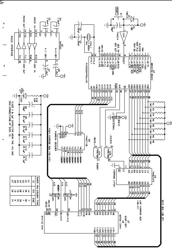
The circuit has five major components: the 8052-BASIC chip (U2), an address latch (U4), an address decoder (U6), static RAM (U7), and an RS-232 interface (U5). As I’ll explain below, a few of the components aren’t essential at this point, but I’ve included them to allow easy expansion later on.
The circuit configuration is a more-or-less standard design, similar to many other microcontroller circuits. When you understand this circuit, you’re well on your way to understanding many others.
The following paragraphs explain the circuit operation, component by component. If you’re impatient to get started, you can skim or skip over this section for now, and go straight to the construction details.
The Microcontroller Idea Book |
23 |
Chapter 3
24 |
The Microcontroller Idea Book |

Powering Up
Table 3-1. |
Parts list for Figure 3-1’s circuit. |
Semiconductors |
|
LED1 |
Light-emitting diode |
U1 |
74HC14 quad inverting Schmitt trigger |
U2 |
8052-BASIC or 80C52-BASIC microcontroller |
U3 |
74HCT08 quad AND gate |
U4 |
74HCT373 octal transparent latch |
U5 |
MAX232, RS-232 driver/receiver |
U6 |
74HCT138 3-to-8-line decoder |
U7 |
6264 (8 kilobyte) or 62256 (32 kilobyte) static RAM, access time 250ns or |
|
less |
Resistors (1/4-watt, 5% tolerance) |
|
R1-R9 |
10,000-ohm |
R10 |
330-ohm |
Capacitors (16WVDC, 20% tolerance) |
|
C1,C8 |
10-microfarad, aluminum or tantalum electrolytic |
C2,C3 |
30-picofarad ,ceramic disc |
C4-C7 |
1.0-microfarad,aluminum or tantalum electrolytic |
C9-C13 |
0.1-microfarad, ceramic disc |
Miscellaneous |
|
J1-J3 |
SIP header, 3-terminal, and shorting block |
S1 |
Switch, normally-open momentary pushbutton |
XTAL1 |
11.0592-Mhz crystal |
RS232 connector, IC sockets, perforated board, wire, solder, and other circuit-construction materials
The Microcontroller
U2 is the 8052-BASIC chip. The circuit is designed so that you can use either the NMOS version or the CMOS 80C52-BASIC.
EA, the External Access Enable input (pin 31 of U2), connects to +5V. This causes the 8052 to run the BASIC-52 interpreter in ROM on boot-up. If EA is low, the 8052 ignores its internal ROM and instead accesses external program memory on boot-up. You can wire EA directly
The Microcontroller Idea Book |
25 |

Chapter 3
to +5V, or use a jumper as shown in the schematic, to allow you to bypass BASIC-52 and boot to an assembly-language program in external memory, as described in Chapter 13.
The crystal. XTAL1 is an 11.0592-Mhz crystal that connects to pins 18 and 19 of U2. This crystal frequency has two advantages. It gives accurate baud rates for serial communications, due to the way that the 8052’s timer divides the system clock to generate the baud rates. Plus, BASIC-52 assumes this frequency when it times the real-time clock, EPROM programming pulses, and serial printer port.
However, you should be able to use any crystal value from 3.5 to 12 Megahertz. If you use a different value, you can use BASIC-52’s XTAL operator to adjust the timing to match the frequency of the crystal you are using. The serial communications are reliable if the baud rate is accurate to within a few percent. The higher the crystal frequency, the faster your programs will execute, so most designs use either 11.0592 Mhz or 12 Mhz, which is the maximum clock frequency that the standard 8052 chip can use.
Capacitors C2 and C3 are 30 picofarads each, as specified in the 8052’s data sheet. Their precise value isn’t critical. Smaller values decrease the oscillator’s start-up time, while larger values increase stability.
Reset circuit. A logic high on pin 9 of U2 resets the chip. On power up, pin 1 of U1 rises slowly from 0V to +5V as capacitor C1 charges through resistor R1. Inverter U1 has a Schmitt-trigger input, which has upper and lower switching thresholds that help to ensure a clean reset pulse at pin 9 of U2. On a logic gate that doesn’t have a Schmitt-trigger input, the output may oscillate if a slowly changing input remains near the switching threshold. In contrast, at U1, when pin 1 reaches the upper switching threshold (about 2.8V), pin 2 switches from high to low, but won’t go high again until pin 1 drops to the lower threshold of about 1.8V.
Pressing and releasing S1 resets the 8052-BASIC chip by discharging C1 and then allowing it to recharge, which brings RESET high, then low again
External Memory
The remaining connections to U2 have to do with reading and writing to external memory.
Read and write signals. To enable reading combined program and data memory, AND gate U3A’s output is RDANY. This signal is low when either READ or PSEN is low. Figure 3-1’s circuit doesn’t use RDANY, but I’ve included U3A for future use. Writing to data memory is controlled by WRITE. Code memory can’t be written to.
AD0-AD7 connect to U4, a 74HCT373 octal transparent latch that stores the lower address byte during memory accesses. The chip contains a set of D-type latches that store logic states.
26 |
The Microcontroller Idea Book |
Powering Up
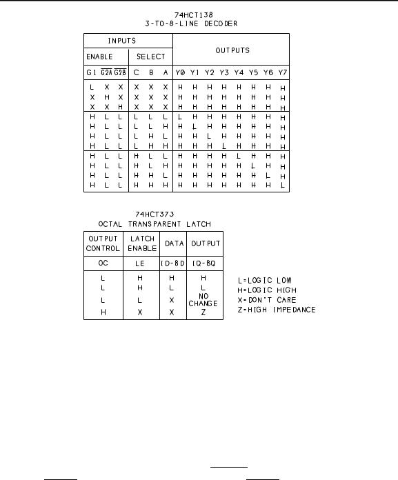
Figure 3-2. Truth tables for the 74HCT138 decoder and 74HCT373 octal transparent latch.
A latch-enable input (LE) controls whether the outputs are latched (stored), or not latched (immediately follow the inputs). Figure 3-2 shows the truth table for the chip. When pin 11 is high, 1Q-8Q follow 1D-8D. When pin 11 goes low, outputs 1Q-8Q will not change until pin 11 goes high again.
During each external memory access, 1Q-8Q store the low address byte, so the eight lines that connect to these outputs carry the label LOW ADDRESS BUS. AND gate U3B latches, or stores, U4’s outputs only when both ALE and ALEDIS are high. During normal memory accesses, ALEDIS remains high, and ALE controls U4. ALEDIS disables the latches when BASIC-52 executes its programming commands. Figure 3-1’s circuit doesn’t use the programming commands, so ALE could control U4 directly, but again, I’ve included U3B for future use.
Because AD0-AD7 hold the data to be read or written during a memory access, the signals as a group carry the label DATA BUS. Each line of AD0-AD7 has a 10K pullup resistor. These are
The Microcontroller Idea Book |
27 |

Chapter 3
required for the programming functions, and are included for future use. You can use eight individual resistors, or a resistor network that contains eight resistors in a SIP or DIP package. In a bussed resistor network, one pin connects to one side of all of the resistors, so you have fewer connections to wire.
The remaining bus is the HIGH ADDRESS BUS (A8-A15), which consists of the upper eight address lines, and is not multiplexed.
Address decoding. U6 is a 74HCT138 3-to-8-line decoder. It functions as an address decoder for the 64K external memory space. Address decoding allows multiple chips to connect to the address and data buses, with each chip enabled only when it is selected.
Figure 3-2 shows a truth table for the decoder. The 8052-BASIC chip uses the three highest address lines (A13-A15) to generate a chip-select signal for each of eight 8K blocks in memory. This is by no means the only way to decode memory, but it’s a common and flexible one. In the schematic, each output is labeled with the base, or bottom, address in the block it controls.
For example, when U2 reads or writes to an address between 0 and 1FFFh in external memory, A13, A14, and A15 are low, so pin 15 of U6 is low. For all other addresses, pin 15 is high. If we connect pin 15 to the chip-select input of an 8K RAM, the RAM will be enabled only when addresses from 0 to 1FFFh are accessed. (Remember that 8K, or 8 kilobytes, is 2000h, or 0 through 1FFFh, in hexadecimal.)
If you use a 32K RAM, you don’t need U6 to decode its addressing. For all of the 32K RAM’s addresses (0 to 7FFFh), A15 is low, and for all other addresses (7FFFh to FFFFh), A15 is high. This means that you can use A15 directly as a chip select, without additional decoding. U6 will come in handy later, however, even if you use a 32K RAM.
RAM choices. The minimal circuit includes just one memory chip, U7, which can be an 8K or 32K static RAM, or SRAM. BASIC-52 requires at least 1K of RAM, but I’ve used the larger capacities, since the extra room is useful and doesn’t cost much more. The pinouts of the two chips are similar, with jumpers J2 and J3 routing the signals that vary.
The 8K chip has 13 address inputs (A0-A12), while the 32K chip has 15 (A0-A14). Eight data I/O pins (I/O1-I/O8) connect to the data bus and hold the bytes to be read or written.
The RAM has three control inputs whose functions match those of the 8052’s control outputs. Pin 20 (CS1, or Chip Select 1) enables U7 whenever the 8052 reads or writes to the chip, with the address decoding determining the address range of the chip.
28 |
The Microcontroller Idea Book |
Powering Up
Jumper J3 chooses the chip select for an 8K or 32K device. Some 8K RAMs have a second chip select (CS2), which is tied high (always selected) by J2. If you limit yourself to either 8K or 32K RAMs, you can eliminate J2 and J3 and wire the appropriate connections directly.
Pin 27 (WE, or Write Enable) is driven by WRITE, and is strobed low during each write to external data memory. Pin 22 (OE, or Output Enable) is driven by READ, and strobes low when either external data or code memory is read.
With an 8K RAM, each write cycle follows this sequence: The 8052 brings ALE high and places the address to be written to on AD0-AD7 and A8-A15. For addresses from 0 to 1FFFH, A13-A15 are low, so U7 is selected at its pin 20. After a short delay, the 8052 brings ALE low, which causes U7 to store the lower address byte. After another short delay, the 8052 replaces the address on AD0-AD7 with the data to be written. A low pulse at pin 27 (WE) causes the RAM to write the data into the address specified by A0-A12.
Read cycles are similar, except that a pulse at pin 22 (OE) causes the requested data to appear on AD0-AD7, where the 8052 reads it.
With a 32K RAM, the process is the same, except that A15 is the chip select and there are two more address lines on the chip.
Static RAM chips are rated by their read-access time, which is the maximum time the chip will require to place a byte on the data bus after a read is requested. With a crystal frequency of 12 Mhz or lower, an access time of 250 nanoseconds or less is fine for accessing external data or code memory. Access times and other timing characteristics are described in the timing diagrams in the data sheets for the 8052 and RAM.
When you use the 8052-BASIC, you don’t have to worry about any of these specifics about the read and write cycles. If the circuit is wired correctly, and if all of the components are functioning as they should, reading and writing occur automatically in the course of executing BASIC-52 statements and commands. A single program line in BASIC-52 can cause dozens or more read and write operations to occur.
Logic families. Logic chips U3, U4, and U6 are HCT-family components, which have TTL-compatible inputs and CMOS-compatible outputs. This means that they can interface directly to either TTL or CMOS logic.
If HCT-family parts aren’t available, there are alternatives. You may use an LSTTL chip (74LS08, 74LS138, 74LS373) for U3, U4, or U6. Or, if you use a CMOS 80C52-BASIC for U2, you may use an HCMOS 74HC08 or 74HC138 for U3 or U6. If U3 is a 74HC08 or 74HCT08, you may use a 75HC373 for U4. For U1, you may use a 74HC14 or 74LS14.
The Microcontroller Idea Book |
29 |