

The Microcontroller Idea book (Jan Akelson, 1997)
.pdfChapter 6
90 |
The Microcontroller Idea Book |

Inputs and Outputs
U11 is a 74HCT138 3-to-8-line decoder that generates individual chip-enable signals for eight 1K blocks in the memory area from E000h to FFFFh. It works the same way that U6 generates chip selects for 8K blocks in the main circuit.
U11 is enabled whenever pin 7 of U6 is low, which occurs when the 8052-BASIC reads or writes to addresses from E000h to FFFFh.
Address lines A10, A11, and A12 determine which of U11’s outputs goes low when the chip is enabled. As with U6, each output is low for a different memory area. For example, pin 15 is low only when addresses from E000h to E3FFh are being read or written to.
One possible point of confusion is that both pin 7 of U6 ( in Figure 3-1) and pin 15 of U11 are chip-selects with a starting address of E000h. One controls memory accesses in the entire 8K block from E000h to FFFFh, while the other controls only the 1K block from E000h to E3FFh. To distinguish the two, I’ve labeled U11’s pin 15 as E000H-1K.
U12 and U14 are examples of input and output ports that U11 can enable.
An Input Port
U12 is a 74LS244 octal buffer that adds eight inputs to the circuit. The buffer’s Y outputs connect to the system’s data bus (D0-D7). The chip has two groups of four buffers, with each having its own enable input (1G and 2G). For this application, the enables are tied together, and all eight buffers are accessed as a group.
I used an LSTTL device for the buffer rather than a CMOS 74HC244 for a couple of reasons. The LSTTL chip has Schmitt-trigger inputs, which are less sensitive to noise. Plus, unlike CMOS, the LSTTL buffer requires no pull-up resistors at unused inputs.
OR gate U9B ensures that U12 is enabled only when U2 (the 8052-BASIC chip) reads an address from E000h to E3FFh. When this occurs, output-enable pins 1 and 19 go low, the buffer’s outputs follow its inputs, and U2 reads the data that U12 has placed on D0-D7.
After a read operation, pins 1 and 19 go high and U12’s outputs are high-impedance. In other words, the outputs are electrically similar to an open circuit, which ensures that they won’t interfere with other operations on the data bus.
In the circuit, U12 is read-only. Write operations to E000h have no effect. To access U12 at a different address, wire pin 4 of U9B to a different output of U11.
Memory decoding options. Note that although U12 holds just one byte of information to read, you can access it at any address from E000h to E3FFh. This may seem like a waste of
The Microcontroller Idea Book |
91 |

Chapter 6
1023 (3FEh) addresses. Indeed, if using every byte of memory is critical, you can use other methods in place of U11 to more completely decode, or divide, the memory space.
Programmable logic is one possibility, for those who have access to a logic compiler and device programmer. But for many circuits, complete decoding of memory isn’t necessary, and less-than-complete decoding using off-the-shelf parts is more practical.
An Output Port
To complement U12’s input byte, U14 provides eight bits of output. U14 is a 74LS374 octal flip-flop, which is very similar to the 74HCT373 octal latch at U4. On the ’373, 1Q-8Q follow 1D-8D until pin 11 goes high, after which 1D-8D no longer change. In contrast, on the ’374, 1Q-8Q change only on pin 11’s rising edge, when 1D-8D are latched to 1Q-8Q.
Here again, I chose LSTTL over CMOS, this time because the LSTTL device can sink 12ma at 0.25V, compared to 6ma at 0.2V for the 74HC374. However, the 74HC374 can also source 6ma at 4.2V, so it’s a better choice if you need to draw current from a logic-high output.
U14’s eight data inputs connect to the data bus (D0-D7). Its output control (pin 1) is tied low so that the outputs are always enabled. If you want to be able to disable the outputs, you can instead tie pin 1 to an unused bit on Port 1.
NOR gate U13A clocks U14 only when U2 writes to addresses from E400h to E7FFh. When this occurs, the data written is latched to the outputs of U14. The outputs do not change until the next time the chip is written to.
In the circuit, U14 is write-only. Reading address E400h will return the value 0FFh. To access U14 at a different address, wire pin 2 of U13A to a different output of U11.
Since U12 is read-only and U14 is write-only, you could use the same address for both, by having them share the same output of U11. For example, if you wire both pin 2 of U13A and pin 4 of U9B to pin 7 of U11, both will be accessed at FC00h. Write operations will access U12, and reads will access U14. In this way, you can add up to eight input ports and eight output ports, with eight chip-select addresses in all.
Wiring Tips
Add Figure 6-2’s circuits to Chapter 3’s circuits, including the connections shown to D0-D7, A10-A12, E000h, READ, and WRITE in the main circuit. The schematic continues the component numbering sequence from the earlier schematics. Use sockets for the ICs. Wire U13’s unused inputs (pins 5, 6, 8, 9, 11, and 12) to GND or +5V. Also add a couple of 0.1-microfarad ceramic decoupling capacitors from +5V to GND, near the added ICs.
92 |
The Microcontroller Idea Book |

Inputs and Outputs
If you wish, you can wire U14’s inputs and U12’s outputs to headers for easy access when you want to connect clip-on jumpers, probe leads, or ribbon cables to the inputs and outputs.
Basic Tests
What can you do with these new inputs and outputs? First, some simple tests. You read and write to the ports exactly as you read and write to external memory. This BASIC-52 statement will display the value of the byte at U12’s inputs:
PRINT XBY(0E000h)
Or, you may prefer a hexadecimal display:
PH0. XBY(0E000h)
To verify that you’re reading all bits correctly, jumper each input in turn to ground and +5V and read the results. Open inputs are undefined and may read as high or low.
To test U14’s outputs, use this BASIC-52 statement:
XBY(0E400h)=xx
where xx is the value you want to write to the chip. To set all bits, write 255 or 0FFh. To clear them, write 0. To verify that all bits are responding, connect a logic probe, voltmeter, or oscilloscope to each of the outputs of U14 in turn and verify that the bits respond correctly to your commands.
Input Examples
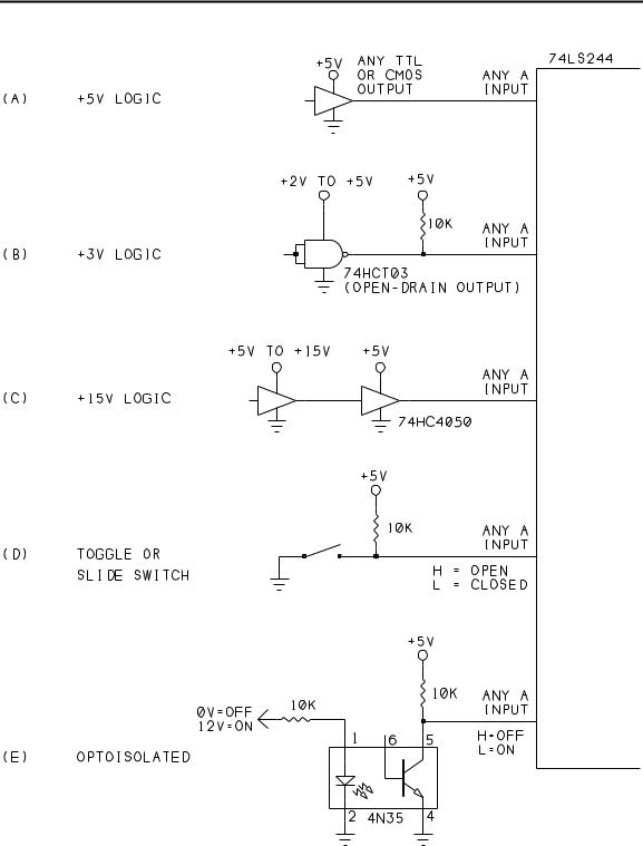
Figure 6-3 shows some inputs that you can interface to U12.
(A)TTL or CMOS logic outputs powered at 5 volts can directly drive U12’s inputs.
(B)To translate lower voltages to 5-volt logic, use a 74HCT03 or similar open-drain NAND gate with a pullup resistor to 5 volts.
(C)To translate higher voltages to 5-volt logic, use a 74HC4050 buffer or 74HC4049 inverter, powered at 5 volts. These chips can safely accept inputs up to 15 volts.
(D)You can also detect the state (open or closed) of a toggle or slide switch at a port pin.
(E)An optocoupler is another way to interface different voltage levels, and it also electrically isolates the input from the microcontroller circuit.
The Microcontroller Idea Book |
93 |
Chapter 6
Figure 6-3. Input interfaces for the 74LS244 buffer.
94 |
The Microcontroller Idea Book |
Inputs and Outputs
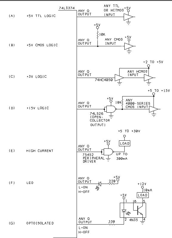
Figure 6-4. Output interfaces to the 73LS374 octal latch.
The Microcontroller Idea Book |
95 |

Chapter 6
Output Examples
Figure 6-4 shows some basic outputs that you can connect to U14:
(A)Outputs can directly drive any TTL or HCTMOS logic input powered at 5 volts.
(B)To interface to 5-volt HCMOS or 4000-series CMOS devices, add a pull-up resistor to ensure that high outputs are greater than 3.5 volts.
(C)To translate an output to a lower voltage, use a 74HC4050 buffer or 74HC4049 inverter powered at the lower voltage.
(D)To translate an output to a higher voltage, use a 74LS26 NAND or similar high-voltage, open-collector gate, with a pullup resistor to the higher voltage.
(E)For high-current outputs, you can use Texas Instruments’ 7545X series of peripheral drivers. The 75452 NAND gate can sink up to 300 milliamperes at 0.5V.
(F)U14 can directly drive an LED. Since the 74LS374 can sink more current than it can source, connect the LED so that it turns on when the output is low. With a 220-ohm current-limiting resistor, the LED’s forward current is around 13 milliamperes.
(G)As with inputs, an optocoupler is another way to interface different voltages, and to electrically isolate an output from the microcontroller circuit.
Reading and Controlling Individual Bits
Unlike assembly language for the 8052, BASIC-52 has no logical operators for setting and clearing individual bits in a byte. But you can use the .AND. and .OR. operators to accomplish the same thing.
Listing |
6-1. Displays the value of each bit at input port E000h. |
|
10 |
A=XBY(0E000H) |
|
20 |
PRINT “Bit 0 = ”,(A.AND.1) |
|
30 |
PRINT “Bit 1 = ”,(A.AND.2)/2 |
|
40 |
PRINT “Bit 2 = ”,(A.AND.4)/4 |
|
50 |
PRINT “Bit 3 = ”,(A.AND.8)/8 |
|
60 |
PRINT “Bit 4 = ”,(A.AND.10H)/10H |
|
70 |
PRINT “Bit 5 |
= ”,(A.AND.20H)/20H |
80 |
PRINT “Bit 6 |
= ”,(A.AND.40H)/40H |
90 |
PRINT “Bit 7 |
= ”,(A.AND.80H)/80H |
100 |
END |
|
96 |
The Microcontroller Idea Book |

Inputs and Outputs
Listing 6-2. Sets or clears a bit at output port E400h.
5 |
REM variable A contains the last data written to 0E400h |
10 |
INPUT “Enter a bit to set or clear (0-7) :”,X |
20 |
INPUT “Enter 1 to set, 0 to clear :”,Y |
30 |
IF Y=1 THEN A=A.OR.2**X |
40 |
IF Y=0 THEN A=A.AND.0FFH-2**X |
50 |
XBY(0E400H)=A |
60 |
END |
Listing 6-1 is a program that reads the buffer and displays the value of each bit. The program is similar to Listing 3-1, which displays the bit values at Port 1.
Line 20 finds the logic state of bit 0 by logically ANDing the byte with a mask byte that is all 0’s except for bit 0: 00000001. The result is 1 if bit 0 is 1, and 0 if bit 0 is 0. Lines 30-90 are similar, except that each time a different bit in the mask byte is 1. In each case, the program divides the result by 2 raised to the power of the bit number. Since (2**0 equals 1, line 20 leaves out this step.) Each PRINT statement shows the logic state of one of the bits.
At the output port, if you want to change just one bit in the byte, you have to know the current value of the byte. The simplest way to accomplish this is to save the last value you wrote. Or, you could wire an input buffer at the same address, with each input bit connecting to the corresponding output bit, and read the input when you need to know the current value.
Listing 6-2 prompts you for a bit to set and clear, then does so. It assumes that you’ve stored the current value of E400h in variable A.
To set a bit, line 30 logically ORs the current value with a mask byte that is all 0s except for the bit to be set. For example, to set bit 4, the mask byte is 0001 0000, or 10h, which leaves bits 0-3 and 5-7 unchanged, but forces bit 4 to be 1.
To clear a bit, line 40 logically ANDs the byte with a mask byte that is all 1s except for the bit or bits to be cleared. For example, to clear bit 3, the mask byte is 1111 0111, or F7h. The result is that bits 0-2 and 4-7 are unchanged, but bit 3 must be 0.
Line 50 writes the new byte to the port.
The Microcontroller Idea Book |
97 |

Chapter 6
Table 6-1. Popular peripheral interface chips.
8253/4Programmable Interval Timer
Three independent 16-bit counters, 6 modes, up to 10 Mhz
8255 Programmable Peripheral Interface
Three 8-bit I/O pins, 3 modes, direct bit set/reset ability
8256 Multifunction Microprocessor Support Controller
Asynchronous serial interface, baud rate generator, five 8-bit timer/counters, two 8-bit I/O ports, 8-level interrupt controller, programmable system clock
8259 Programmable Interrupt Controller
Eight-level priority controller, programmable interrupt modes
8279 Programmable Keyboard/Display Interface
Scanned interfaces to 64-contact key matrix and 16-character display.
The 8255 Programmable Peripheral Interface
In addition to the inputs and outputs provided by U12 and U14, there are specialized peripheral-interface chips that you can add to your system. Table 6-1 lists several examples.
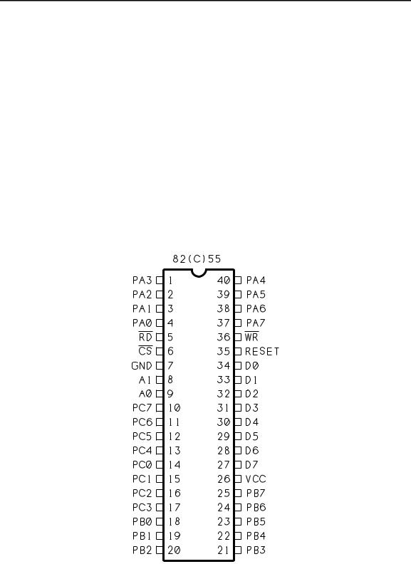
One of the most popular of these is the 8255 programmable peripheral interface, or PPI. Figure 6-5 shows the pinout, and Table 6-2 shows the pin functions. The chip adds 24 bits of I/O, plus the option to use special control and handshaking signals to communicate with peripherals.
Intel originally introduced the 8255 as a peripheral for its 8085 microprocessor, but it remains
a popular chip for use with 8052s and other computer chips. Manufacturers of compatible chips include AMD, OKI, Toshiba, and NEC, which calls its chip the PD71055.
If you use the 8255, you’ll want a copy of its data sheet, which more fully explains its abilities and configuration options.
8255 Variants
You have a choice of the original NMOS 8255 or the CMOS 82C55. The CMOS version usually costs a little more, but has some advantages. First, it has lower power consumption, with supply currents of 10 milliamperes (10 microamperes in standby mode with CS=high), compared to 120 milliamperes for the 8255.
98 |
The Microcontroller Idea Book |
Inputs and Outputs
The 82C55 also has CMOS-compatible outputs, which means that they can drive either LSTTL or CMOS inputs. When driving CMOS inputs, the NMOS 8255’s outputs should have pull-up resistors to ensure that high outputs are at least 3.5 volts.
A third advantage to the 82C55 is greater current-sourcing ability, which can be important if you want to directly drive a transistor or source more than a fraction of a milliampere. Intel’s 82C55 can source 2.5 milliamperes at 3 volts, compared to just 0.4 milliamperes at 2.4 volts for the 8255. However, NEC’s CMOS 71055 has the same current-sourcing ability as the NMOS 8255, so it depends on the manufacturer. All can sink 2.5 milliamperes at 0.45 volts. The 74LS374 latch (U14) has greater output drive ability than any of the 8255s.
Speed Ratings
The 8255 is also available with different speed ratings, including 3 Mhz and 5 Mhz. The 5-Mhz part is sometimes called the 8255-5. From the ratings, it may seem that the 8255 is too slow to interface to a 12-Mhz 8052-BASIC. But what does the speed rating actually refer to? Since the 8255 was developed for the 8085, I suspect that it refers to the maximum
Figure 6-5. Pinout of the 8255 Programmable Peripheral Interface.
The Microcontroller Idea Book |
99 |