

PART II
The Software
In Part I we developed the concept of the Havard architecture, ending up with our somewhat simplified BASIC computer. Although BASIC was entirely fictitious, it was designed with an eye to the MCU that forms the basis for the rest of this book.
This part of the text looks mainly at the software aspects of our chosen MCU, the mid-range Microchip PIC family. We will be covering:
•The internal structure of the MCU.
•The instruction set.
•Address modes.
•The assembly translation process.
•Subroutines and modular program design.
•Interrupt handling.
•The high-level language C.
CHAPTER 4
The PIC16F84 Microcontroller
In this chapter we introduce the PIC16F84 MCU, which we will use as our baseline exemplar for the rest of the text. Here we will primarily look at internal structure, reserving external interfacing considerations for Part 3 of the book.
After reading this chapter you should:
•Recognize the di erence between a microprocessor and microcontroller.
•Understand the Harvard-based architecture with its parallel fetch and execute units.
•Appreciate the function, structure and memory map of the unrelated Program and Data stores.
•Be able to interpret the Status register bits that control memory paging and hold the C, DC and Z flags.
•Know how to manipulate the contents of the Program Counter in conjunction with the PCLATH special-purpose file register.
•Understand the interaction between the clock phases and the internal sequence of micro-operations.
•Appreciates the principle of banking in the Data store and its relationship to the RP0 control bit in the Status register.
•Know what peripheral functions are integral to the PIC16F84.
What exactly is a microcontroller unit? In a nutshell, a microcontroller is a MicroProcessor Unit (MPU) which is integrated with memory and input/output peripheral interface functions on the (usually) one integrated circuit. In essence it is a MPU with on-board system support circuitry. Thus we begin by investigating the origins of the MPU. From a historical perspective the story begins in 1968 when Robert Noyce (one of the inventors of the integrated circuit), Gordon Moore1 and Andrew Grove left the Fairchild Corporation and founded their own company, which they called Intel.2 Within three years, Intel had developed all the basic types of semiconductor memories used today – dynamic and static RAMs and EPROMs.
1Moore’s law stated in 1964 that the number of elements on a chip would double every 18 months, although this was subsequently revised to 2 years.
2Reputed to stand for INTELligence or INTegrated ELectronics.

78 The Quintessential PIC Microcontroller
As a sideline Intel also designed large-scale integrated circuits to customers’ specifications. In 1970 they were approached by the Nippon Calculating Machine Corporation, and asked to manufacture a suitable chip set for a line of calculators to be named Busicom. At that time calculators were a fast-evolving product and any LSI devices were likely to be superseded within a few years. This of course would reduce an LSI product’s profitability and increase its cost. Engineer Ted Ho – reputedly while on a topless beach in Tahiti – came up with a revolutionary way to tackle this project. Why not make a simple computer central computing unit (CPU) on silicon? This could then be programmed to implement the calculator functions, and as time progressed these could be enhanced by developing this software. Besides giving the chip a longer and more profitable life, Intel were in the business of making memories – and computer-like architectures need lots of memory. Truly a brain wave. The Japanese company endorsed the Intel design for its simplicity and flexibility in late 1969, rather than the conventional implementation.
Federico Faggin joined Intel in spring 19703 and by the end of the year had produced working samples of the first chip set. This could only be sold to the Nippon Calculating Machine Corporation, but by the middle of 1971, in return for a price reduction, Intel were given the right to sell the chip set to anyone for non-calculator purposes. Intel was dubious about the market for this device, but went ahead and advertised the 4004 “Micro-Programmable Computer on a Chip” in the Electronic News of November 1971. The term microprocessor unit was not coined until 1972. The 4004 created a lot of interest as a means of introducing ‘intelligence’ into electronic products.
The 4004 MPU featured a von Neumann architecture using a four-bit data bus, with direct addressing of 512 bytes of memory. Clocked at 108 kHz, it was implemented with a transistor count of 2300.4 Within a year the eight-bit 200 kHz 8008 appeared, addressing 16 Kbytes and needing a 3500 transistor implementation. Four bits is satisfactory for the BCD digits used in calculators but eight bits is more appropriate for intelligent data terminals (like cash registers) which need to handle a wide range of alphanumeric characters. The 8008 was replaced by the 80805 in 1974, and then the slightly modified 8085 in 1976. The 8085 is still the current Intel eight-bit device. Strangely, 4-bit MPUs were to outsell all other sizes until the early 1990s.
The MPU concept was such a hit that many other electronic manufactures clambered on to the bandwagon. In addition, many designers jumped ship and set up shop on their own, such as Zilog. By 1976 there
3He was later to found Zilog (last word (Z) in Integrated LOGic) which became notable with the Z80 MPU – a rather superior Intel 8085.
4Compare with the Pentium Pro (also known as the P6 or 80686) at around 5.5 million! 5Designed by Masatoshi Shima, who went on to design the 8080-compatible Z80 for
Zilog.

4. The PIC16F84 Microcontroller 79
were 54 di erent MPUs either available or announced. For example, one of the most successful families was based on the 6800 introduced by Motorola.6 The Motorola 6800 had a clean and flexible architecture, could be clocked at 2 MHz and address up to 64 Kbyte of memory. The 6802 (1977) even had 128 bytes of on-board memory and an internal clock oscillator. By 1979 the improved 6809 represented the last in the line of these eight-bit devices, competing mainly with the Intel 8085, Zilog Z80 and MOS Technology’s 6502.
The MPU was not really devised to power conventional computers, but a small calculator company called MITS,7 faced with bankruptcy, took a final desperate gamble in 1975 and decided to make and market a computer. This primitive machine, designed by Ed Roberts, was based on the 8080 MPU and interacted with the operator using front panel toggle switches and lamps – no keyboard and VDU. The Altair8 was advertised for $500, and within a month MITS had $250,000 in the bank for advance orders.
This first Personal Computer (PC) spawned a generation of computer hackers. Thus an unknown 19-year-old Harvard computer science student, Bill Gates, and a visiting friend, Paul Allen, in December 1975 noticed a picture of the Altair9 on the front cover of Popular Electronics and decided to write software for this primordial PC. They called Ed Robert with a blu , telling him that they had just about finished a version of the BASIC programming language that would run on the Altair. Thus was the Microsoft Corporation born.
In a parallel development, 22 Altair owners in San Francisco set up the Home-brew club. Two members were Steve Jobs and Steve Wozniak. As a club demonstration, they built a PC which they called the Apple.10 By 1978 the Apple II made $700,000; in 1979 sales were $7 million, and then $48 million…
The Apple II was based around the low-cost 6502 MPU which was produced by a company called MOS Technology. It was designed by Chuck Peddle, who was also responsible for the 6800 MPU, and had subsequently left Motorola. The 6502 bore an uncanny resemblance to the Motorola 6800 family and indeed Motorola sued to prevent the related 6501 MPU being sold, as it even had the same pinout as the 6800. The 6502 was one of the main players in PC hardware by the end of the 1970s, being
6Motorola was launched in the 1930s to manufacture motor car radios, hence the name “motor” and “ola” – as in pianola. It has the largest share of the world-wide microcontroller market at the time of writing (1999).
7Located next door to a massage parlor in New Mexico. 8After a planet in Star Trek.
9The picture was just a mock up, they actually were not yet available; an early example of computer ‘vaporware’!
10Jobs was a fruitarian and had previously worked in an apple orchard.

80 The Quintessential PIC Microcontroller
the computing engine of the BBC series and Commodore PETs amongst many others.
What really powered up Apple II sales was the VisiCalc spreadsheet package. When the business community discovered that the PC was not just a toy, but could do ‘real’ tasks, sales took o . The same thing happened to the IBM PC. Reluctantly introduced by IBM in 1981, the PC was powered by an Intel 8088 MPU clocked at 4.77 MHz together with 128 Kbyte of RAM, a twin 360 Kbyte disk drive and a monochrome textonly VDU. The operating system was Microsoft’s PC/MS-DOS version 1.0. The spreadsheet package here was Lotus 1-2-3.
By the end of the 1970s the technology of silicon VLSI fabrication had progressed to the stage that several tens of thousands transistors could be integrated on the one chip. Microprocessor designers were quick to exploit this capability in one of two ways. The better known of these was to increase the size of the ALU and buses/memory capacity. Intel were the first with the 29,000-transistor 8086, introduced in 1978 as a 16-bit version of the 8085 MPU.11 It was designed to be compatible with its eight-bit predecessor in both hardware and software aspects. This was wise commercially, in order to keep the 8085’s extensive customer base from looking at competitor products, but technically dubious. It was such previous experience that led IBM to use the 8088 version, which had a reduced eight-bit data bus and 20-bit address bus12 to save board space.
In 1979 Motorola brought out its 16-bit o ering called the 68000 and its eight-bit data bus version, the 68008 MPU. However, internally it was 32-bit, and this has provided compatibility right up to the 68060 introduced in 1995 and ColdFire RISC device launched in 1997. With a much smaller eight-bit customer base to worry about, the 68000 MPU was an entirely new design and technically much in advance of its 80X86 rivals.
The 68000 was adopted by Apple for its Macintosh series of PCs. However, the Apple Mac only accounts for less than 5% of PC sales. Motorola MPUs have been much more successful in the embedded microprocessor market, the area of smart instrumentation from egg timers to aircraft management systems. Of course, this is just the area which MPUs were developed for in the first place, and the number, if not the profile and value, of devices sold for this purpose exceeds those for computers by more than an order of magnitude.
In this applications area an MPU is ‘buried’ in the application circuit together with memory and various input and output interface circuits. The MPU with its program acts as the controller of the system by virtue of the software in program memory. Over 3.5 billion microprocessor and
11and the Intel 8086 architecture-based MPUs are by far the largest selling MPU for computer-based circuitry.
12A 220 address space is 1 Mbyte, and this is why for backwards compatibility MS-DOS was limited to 1 Mbyte of conventional memory.
4. The PIC16F84 Microcontroller 81
related devices are sold each year for embedded control, making up over 90% of the MPU market.
The second way of using the additional integrated circuit complexity that became available by the end of the 1970s was to keep a relatively simple CPU and use the extra silicon ‘real estate’ to implement on-board memory and input/output interface. In doing so, simple embedded control systems on the one chip became possible and the overall chip count to implement a given function was thereby considerably reduced. The majority of control tasks require relatively little computing power, but the reduction in size (and therefore cost) is vital. A simple example of this is the intelligent smart card, which has a processor integrated into the card itself. Such microprocessor-based devices were called MicroController Units (MCUs).13 For example there are about 100 microcontrollers hidden in every home; in the washing machine, microwave oven, telephones, electronic games and so on. About 20 more lurk in the average family car.14
|
|
|
Microcontroller |
|
|
|
G5 |
MPU |
|
|
|
|
|
|
|
Gearbox |
G4 |
Input |
SRG49 |
|
G2 |
|||
|
|
G3 |
|
|
|
|
|
|
D |
|
|
|
ports |
Odometer |
|
|
G1 |
Output |
|
|
|
|
|
|
Reset trip |
|
|
ports |
|
|
mi/km |
|
|
|
|
|
|
SRG28 |
|
|
|
|
Counter |
|
Tacho |
pulse |
|
D |
|
|
|
|||
|
|
Trip |
||
|
|
|
|
|
|
|
|
program |
|
|
|
|
memory |
|
Data memory
Non-volatile
store
Fig. 4.1 An example of a system based on a microcontroller.
13The term microcomputer was an alternative term but was easily confused with early personal computers and has dropped into disuse.
14New Scientist, vol. 59, no. 2141, 4th July 1998, pp. 139.

82 The Quintessential PIC Microcontroller
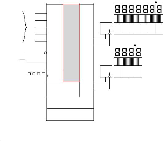
In terms of architecture, referring back to Figs. 3.1 and 3.2 on pages 42 and 44 respectively, the microprocessor is the central processor unit, whereas the microcontroller is the complete functioning computer-like system. As an example, consider the electronics of a car odometer monitoring system displaying total distance since manufacture and also a trip odometer. The main system input signal is a tachometer generating pulses on each rotation of the engine flywheel, which when totalized gives the number of engine revolutions – and the pulse to pulse duration could also give the road speed. Of course the actual road distance depends on the gearing of the engine, and thus we need to know which of the five gear ratios has been chosen by the driver at any time. This is shown as five lines G1…G5 originating from the gear box. One signal will be high for the appropriate forward gear, with neutral and reverse being ignored. Additional inputs are used to give a manufacturer’s option of a mile or kilometer display, and a user input to reset the trip display to zero.
The display itself consists of seven 7-segment digits (see Fig. 6.6 on page 148) to indicate up to (optimistically) 


 .
.
 . As there are so many segments to control (49 in total), Fig. 4.1 shows the display data fed via a single digital line, shunted serially into a shift register – see Fig. 2.20 on page 36. A second line provides clock pulses for the register with 49 clock pulses being needed to refresh the display.15
The trip odometer display comprises four digits, which will record up to 


 .
.
 . Similarly two output lines are used to feed and clock the shift register, and 28 clock pulses are needed to shift in a new 4-digit trip display.
The resource budget (list of subsystem functions) for this system is:
•An edge-triggered input for the tachometer pulse train, connected to a counter/timer to totalize engine revolutions.
•Seven static digital input lines to interface to the gear ratio, mi/km option and trip reset.
•Four output digital lines to clock the two shift registers and provide segment data.
•A microprocessor to do the calculations and to read/write to the input/ output ports respectively.
•Program memory, usually ROM of some kind.
•Data memory for temporary storage of program variables, usually static RAM.
•Non-volatile storage for physical variables, such as total distance and distance since trip reset.
This functionality could be implemented onto a single integrated circuit, and in this situation would be known as a microcontroller, that is a mi-
15Many displays have this shift register built in as a complete subsystem.

4. The PIC16F84 Microcontroller 83
croprocessor integrated with its support circuitry giving a complete microcomputer function. Of course the resource budget listed above is specific to our example. Although the core functions (microprocessor and memory) are common to a wide range of applications, the input/output (I/O) interface needs to be tailored to the task in hand. Some typical I/O functions are:
•I/O to interface to a serial bit stream of various synchronous and asynchronous protocols.
•Counter/timer functions to totalize input events and to generate precision time-varying digital output signals.
•Analog to digital multiplex/conversion to be able to read and digitize analog inputs.
•Digital to analog conversion to output analog signals.
•Display ports to drive multi-digit liquid crystal displays.
This alternative approach to using additional silicon resources led to the first MCUs in the late 1970s. For example the 35,000 transistor Motorola 6801, designed in response to a specific application from an car manufacturer, used the existing 6800 MPU as a core, with 2048 bytes of ROM program memory, 128 bytes of data RAM, 29 I/O lines and a 16bit timer. With the viability of the MCU approach vindicated, a range of families, each based on a specific core but with individual family members having a di erent selection of I/O facilities, was introduced by the leading MPU manufacturers. For example, the Motorola 68HC11 family (a development of the 6801 MCU) uses a slightly enhanced 6800 core. The 68HC12 and 68HC16 families use 16-bit cores but are designed to be upwardly compatible with the 8-bit 68HC11. It was quickly realised that many embedded applications did not even need the power of the (antique) 6800 core, and the 68HC05 family16 had a severely reduced core by lower price. Actually 4-bit MCUs outsold all other kinds of processor until the early 1990s and 8-bit MCUs, now the most popular, are likely to continue in this role for the foreseeable future.
All these MPUs and MCUs were based on the von Neumann architecture (see Fig. 3.1 on page 42) used by mainframe computers. The alternative Harvard architecture (see Fig. 3.2 on page 44), which is chiefly distinguished by having a separate memory space for program and data, originated at Harvard university for a US Defence department computing project, but was rejected in favor of a rival von Neumann design from Princeton university. The first MPU using this architecture was the Signetics 8X300, and this was adapted by General Instruments in the mid 1970s for use as a Peripheral Interface Controller (PIC) which was designed to be a programmable I/O port for their 16-bit CP1600 MPU.
16The 68HC05 has found a niche as the computing engine of smart cards, where highpower computing is not a priority.
84 The Quintessential PIC Microcontroller
General Instruments sold o their microelectronics division in 1988 to a start up company called Arizona Microchip Technology. Microchip’s main product was, and is still, a series of microcontroller families based on this PIC architecture. Their first family was introduced in 1989 with the PIC16C5X series. These Harvard processors are based on a set of only 33 instructions. All instructions are coded in a single 12-bit word. This use of a primordial instruction set is known as Reduced Instruction Set Computer (RISC) and contrasts with the Complex Instruction Set Computer (CISC) model used in most computers/MPUs where several hundred instructions/modes are provided, and because of their number take several memory words to encode. The combination of single-word instructions, the simplified instruction decoder implicit with the RISC paradigm and the Harvard separate Program and Data buses gives a fast, e cient and cost e ective processor implementation. The PIC16C5XX 12-bit core family features between 512 and 2048-instruction Program stores implemented as One-Time Programmable (OTP) EEPROM (see page 26), 25 to 73 bytes of Data memory, 12 or 20 I/O pins in the 18and 28-pin package respectively, and an 8-bit timer. The PIC12CXXX family are 8-pin equivalents.
By 1992 the PIC16CXXX family family based on a 14-bit core enabled easier addressing of larger Program spaces and additional peripheral devices, such as 16-bit timers and A/D converters as well as interrupt handling. The RISC instruction set is virtually identical to the 12-bit core, with a total of 35 instructions. The 16-bit PIC17CXXX core, introduced in 1997, has 58 instruction, with a multiplying ALU and further interface capabilities. It is complemented by the extended 16-bit core PIC18CXXX family introduced in 1999 with 77 instructions more oriented towards high-level language compiler needs.
Of the three families, the 14-bit core is a good compromise between low-cost and ease of use. The PIC16F84, which is the baseline exemplar of this book, is a member of this mid-range family.
From the software point of view all devices with the same core are identical. However, there is a di erent mix of I/O facilities from the hardware perspective, but with much commonalty. For example, the 16C74 supports an 8-channel analog input port, the PIC16C66 a synchronous serial port and the PIC16F84 a non-volatile data memory. All three devices have similar parallel I/O, timer and interrupt handling facilities.
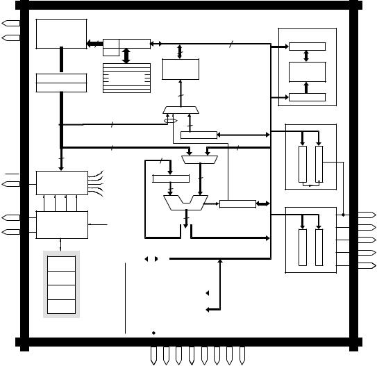
The architecture of the PIC16F84 is shown in a simplified form in Fig. 4.2. Although initially this looks rather complex, it is little more than the architecture of our BASIC computer of Fig. 3.3 on page 45 but with interface ports connected to the internal File store data bus. You should revise this material now as background to our discussion. In essence the PIC family is based on a Harvard structure with its separate Program and Data store, and with peripheral interface ports mapped onto the Data file
4. The PIC16F84 Microcontroller 85
Vdd
14
Vss
5
MCLR
4
OSC1
16
OSC2
15
Program store
Flash ROM
1K x 14
Program 14 data bus 
 Pipeline
Instruction reg 1
Instruction reg 2
op-code 7
Instruction decoder & control
Q1 Q2 Q3 Q4
Oscillator and timing generation
Power-up
timer
Oscillator
start-up
Power-on
Reset
Watchdog
timer
Program |
|
PIC16F84 |
|
EEPROM data memory |
|||||
|
|
|
|
|
|
|
|
|
|
address |
bus |
F 02h |
|
|
File |
data |
bus |
|
F 08h |
Program |
Counter |
|
|
|
|||||
|
|
|
|
|
|
EEPROM data |
|||
13 PLATH |
|
8 |
|
|
|
8 |
|
||
|
|
|
|
|
|
||||
F 0Ah |
|
RAM |
|
|
|
|
|
||
|
|
|
|
Data |
store |
EEPROM |
|||
|
|
|
Register file |
||||||
|
|
|
data memory |
||||||
|
|
|
68 x 8 |
|
|
|
|
||
8-level |
stack |
|
|
|
|
64 x 8 |
|||
|
|
|
|
|
|
||||
|
|
|
8 |
File |
|
|
|
F 09h |
|
|
|
|
address bus |
|
|
EEPROM address |
|||
|
|
|
|
|
|
||||
|
|
|
Address mux |
|
|
|
|
||
7 |
Direct address |
|
8 |
Indirect |
|
|
Timer |
||
|
|
|
|
address |
|
|
|
||
|
|
|
|
|
|
F 04h |
|
|
|
|
|
|
|
File |
select reg. |
|
|
|
|
8 |
Literal data |
|
|
|
|
|
8 File value |
01hF counterTimer 81hF Prescaler |
|
|
|
|
Working reg. |
|
|
|
|
||
|
|
|
8 |
|
Data mux |
|
|
|
|
|
|
|
|
|
|
|
|
||
|
|
|
|
|
|
8 |
|
|
|
|
|
|
8 |
|
|
|
|
|
|
|
|
|
|
|
|
|
|
F 03h |
I/O port A |
|
|
|
|
ALU |
|
RP0 |
Z DC C |
||
|
|
|
|
|
Status |
register |
|
||
|
|
|
|
|
8 |
|
|
||
|
|
|
|
|
|
|
|
|
|
|
|
|
|
|
d |
bit |
|
|
|
SLEEP |
|
|
|
from instruction |
|
|
|||
01
F 0Bh |
|
|
|
TRISA |
F |
A Port |
F |
|
Int control |
|
|
|
|
|
85h |
|
05h |
|
|
|
|
|
|
|||
|
|
|
|
|
|
|
||
|
|
|
|
|
|
|
|
|
F 86h |
|
|
|
|
|
|
|
I/O |
|||
|
|
|
|
|
|
|
TRISB |
|
|
|
|
|
|
|
|
|
port |
|||
|
|
|
|
|
|
|
|
|
|
|
|
|
|
|||||||
|
|
|
|
|
|
|
Port |
|
B |
|
|
|
|
|
|
|
||||
|
|
|
|
|
|
|
|
|
F 06h |
|
|
|
|
|
|
|
|
|||
|
|
|
|
|
|
|
|
|
|
|
|
|
|
|
|
|
|
|
|
B |
|
|
|
|
|
|
|
|
|
|
|
|
|
|
|
|
|
|
|
|
|
|
|
|
|
|
|
|
|
|
|
|
|
|
|
|
|
|||||
|
|
|
|
|
|
|
|
|
|
|
|
|
|
|
|
|
|
|
|
|
|
RB0/INT 6 |
RB1 7 |
RB2 8 |
RB4 10 RB3 9 |
RB5 11 |
RB6 12 |
RB7 13 |
|||||||||||||
RA4/TOCKI
3
RA3
2
RA2
1
RA1
18
RA0
17
Fig. 4.2 Architecture of the PIC16F84 microcontroller
store address space. That is the various ports appear to the software to be in the Data store. In more detail we have:
Central Processor Unit
As a consequence of the Harvard architecture, the CPU is split between the fetch and execution function, both of which operate in parallel with a minimum of interaction.
Fetch
The fetch section comprises a 13-bit Program Counter (PC) addressing the Program store via the Program address bus, and a two-deep Instruction pipeline through which 14-bit instructions via the Program data bus progress through to the Instruction decoder – see Fig. 3.3 on page 45.
The Program Counter is actually located in the Data file store at location File 2 and is labelled as PCL (Program Counter Low byte) in Fig. 4.6.

86 The Quintessential PIC Microcontroller
This means that it can be accessed and manipulated by the software in the same manner as any other file register. For example, if the contents of the Working register were n, then the instruction addwf 2,f (see page 49) overwrites File 2 (i.e. the PC) with its original value plus n – that is skip forward n places. A practical example is given in Program 6.4 on page 149.
There is one problem with this example, which arises because the PC is actually 13-bits wide and File 2 only holds the lower eight bits, PC[7…0]. The upper five bits, PC[12…8] are held in a ‘buried’ register; that is not directly accessible to the programmer. Actually any instruction that directly writes to File 2, such as our example above, does change all 13 PC bits as shown in Fig. 4.3. Not only will the 8-bit outcome of the instruction addwf 2,f be placed in the lower byte of the PC but the lower five bits of the PC bu er register at File 0Ah, labelled PCLATH (for Program Counter LATch High byte) in Fig. 4.3, are automatically copied into the high byte of the Program Counter. The PCLATH file data register is cleared when the PIC is reset and so an instruction like our example will usually result in an address in the first 256-byte ‘page’ of program memory unless PLATH is loaded with a non-zero value. Thus care needs to be taken when altering the state of the PC by writing to PCL in this manner; especially if the outcome overflows its 8-bit field. Instructions that indirectly alter the value of the PC, such as goto, will also use part of the contents of PCLATH in updating the PC. Such instructions carry an 11-bit address as part of the instruction code. Here bits PCLATH[4:3] are moved over to the corresponding PC bits 12 & 11 to give a complete 13-bit PC update
– see Fig. 5.4 on page 114.
Associated with the Program Counter is an area of buried storage that can stack up to eight copies of the PC. The current value of the PC is pushed into this stack when a subroutine is called or an interrupt is serviced. Conversely a return from a subroutine or interrupt causes the
|
|
|
|
|
|
|
PCL |
|
|
|
|
12 |
87 |
0 |
|
||||
Program Counter |
|
|
|
|
|
|
|
||
|
|
|
|
|
|
|
|
|
|
|
|
|
|
|
|
|
File 02h |
|
|
|
|
|
|
|
|
|
|
Outcome from ALU. |
|
|
|
|
|
|
|
|
|
||
|
|
|
|
|
|
|
|
For example, |
|
|
|
PCLATH |
|
|
|
|
movwf |
PCL |
|
|
|
|
|
|
|
or |
|
||
7 |
4 |
|
0 |
|
|
||||
|
|
addwf |
PCL,f |
||||||
|
|
|
|
|
|
|
|
||
|
|
|
|
|
|
|
|
|
|
File 0Ah
Fig. 4.3 Showing how all 13 bits of the Program Counter are altered when writing to PCL.
4. The PIC16F84 Microcontroller 87
last stacked PC value to be popped out again into the PC. Details are given in Chapters 6 and 7.
The PIC microcontrollers have an integral oscillator that generates the internal timing sequences. The oscillator frequency fosc is normally controlled by an external crystal (or ceramic)-capacitor network across the device OSC1 and OSC2 pins – see Fig. 10.4 on page 258. A resistorcapacitor connected to OSC1 may be used as the timing elements where lower precision and frequency stability is not an issue. In this case OSC2/CLKOUT outputs a signal of frequency 14 × fosc. Alternatively an external oscillator can be used as the master clock into OSC1/CLKIN. The
PIC16F84 has a maximum frequency fOSC of 10 MHz but there is no minimum. As we shall see (Fig. 10.2 on page 256) the lower the frequency
the smaller is the power consumption. Unless otherwise stated, we will assume a fosc of 4 MHz for the rest of the text.
The internal oscillator/clock circuitry must be configured to the appropriate mode, as described in Fig. 10.5 on page 261. This is normally done when code is blasted into the Program store flash EEPROM. When the PIC is powered up (external supply voltage is applied) a 72 ms internal reset pulse is generated by the Power-up timer after the supply rises above approximately 2 volts, followed by 1024 clock pulses, counted by the Oscillator Start-Up timer to ensure that the internal oscillator has stabilised. This latter guard timer only operates for crystal-type oscillator modes – see Table 86 on page 258. The Power-Up timer does not operate if an external reset is applied to the Master CLeaR (MCLR) pin.
fosc
Q1
Q2
Q3
Q4
Program stream |
|
Fetch inst. n |
|
Fetch inst. n+1 |
|
|
Fetch inst. n+2 |
|
|
Fetch inst. n+3 |
|
||
|
|
|
|
|
|
||||||||
|
|
|
|
|
|
|
|
|
|
|
|
|
|
Execute stream |
|
|
|
|
|
|
|
|
|
|
|
||
|
Execute inst. n |
|
|
Execute inst. n+1 |
|
|
Execute inst. n+2 |
|
|||||
|
|
|
|
|
|
|
|
|
|
|
|
|
|
|
|
Cycle n |
|
Cycle n+1 |
|
Cycle n+2 |
|
Cycle n+3 |
|||||
|
|
|
|
|
|
|
|
|
Time |
|
|
||
|
|
|
|
|
|
|
|
|
|
|
|||
|
|
|
|
|
|
|
|
|
|
|
|||
Fig. 4.4 Internal clock sequencing waveforms.
88 The Quintessential PIC Microcontroller
The clock input/crystal frequency at the OSC1 pin is divided by four to generate four internal non-overlapping quadrature clocks, as shown in Fig. 4.4. The clock-related sequence of operations in the fetch unit are: Q1: Increment the Program Counter and copy onto the Program store
address bus.
Q4: Read the instruction code o the Program store data bus into Instruction register 1 and at the same time move the previous instruction down the pipeline into Instruction register 2, where it is presented to the Instruction decoder.
Execute
The execution circuitry is centered around the Arithmetic Logic Unit (ALU) – see Fig. 2.19 on page 35. The ALU processes data from up to two sources. One of these is the 8-bit Working register. The other can be multiplexed either from a file in the Data store or an 8-bit literal, which is part of the instruction code – see page 107. For example addwf 20h,w and addlw 5 respectively add the contents of W to that of File 20h or the constant 5 to W. The outcome can be switched back into W (eg. addwf 20h,w) or into the register file (eg. addwf 20h,f) as controlled by the single Destination bit in the instruction code – see page 107.
Where an operand is a file, the execution unit can generate the Data store address in one of two ways – see Fig. 4.6.
•Directly via a 7-bit address field in the instruction – see page 107. Seven bits can only directly address up to 128 files. This can be increased to 256 files if the state of the RP0 (Register Page bit 0) bit in the Status register (see Fig. 4.5) is also multiplexed in as part of the Data store address. Where RP0 is zero, then register files 00 – 7Fh can be addressed, this address page being known as Bank 0. With RP0 set to one, then
Bank 1 is addressed, ranging from 80 – FFh; see Fig. 4.6. RP0 is cleared when the PIC is reset and the Bit Set File and Bit Clear File instructions may be used alter its state. For example, bsf 3,5 sets bit 5 (RP0) in the Status register –see Fig. 4.5.
•Indirectly using the File Select Register in conjunction with Indirect addressing, as described in Fig. 3.6 on page 57. In this situation the 8-bit address in the FSR is used to address the Data store whenever the virtual location File 0 is addressed. Here potentially all 256 files in both banks can be addressed irrespective of the state of RP0.
The three flag bits in the Status register STATUS are associated with the ALU, giving status information concerning the outcome from an instruction, as shown in Fig. 4.5.
Carry flag
Bit 0 of the Status register is the C flag. This primarily holds the Carry out from the last addition operation. Subtraction operations activate this bit as the complement of the Borrow out. For example, 24 − 12 = 12B1 and

4. The PIC16F84 Microcontroller 89
12 − 24 = 88B0. C also functions as an input/output bit for the Rotate instructions, as shown in Fig. 3.7 on page 61.
The label R/W ? in Fig. 4.5 indicates that this bit can be read from or written to and has an indeterminate value on a power-up reset – its value does not alter on any other type of reset.
Digit Carry flag
Bit 1 of the Status register is the DC flag. This operates in the same manner as the standard C flag but holds the Carry out from the lower nybble to the upper nybble; that is from bit 3 to bit 4. In the same manner DC holds the complement of the Borrow out from bit 3 to bit 4. Knowledge of the Carry activity between the lower and upper halves of the byte is useful where binary coded decimal data is being manipulated. Here each nybble holds a 4-bit representation of the decimal digits 0…9 (see page 6) and the half carry then indicates carries between decimal decades.
Zero flag
Bit 2 of the Status register is the Z flag. This is set whenever the outcome of the instruction is zero, otherwise it is cleared.
Status register (SR) File 3
|
|
|
7 |
6 |
5 |
4 |
3 |
2 |
1 |
0 |
|
|
|
|
|
|
|
|
|
RP0 |
TO |
PD |
Z |
DC |
C |
|
|
|
|
|
|
|
(R/W 0) |
(R/W 0) |
(R/W 0) |
(R 1) |
(R 1) |
(R/W ?) |
(R/W ?) |
(R/W ?) |
|
|
|
|
|
|
|
|
|
|
|
|
|
|
|
|
|
|
|
Register |
File Bank Select |
|
|
|
|
|
|
|
|
|
|
|
||
|
|
|
|
|
|
|
Carry/Borrow |
|
||||||
Bank 0 |
(File 00 - 7Fh) |
0 |
|
|
|
|
|
|
|
|
|
|
|
|
|
|
|
|
|
|
|
|
Digit Carry/Borrow |
||||||
Bank 1 |
(File 80 - FFh) |
1 |
|
|
|
|
|
|
|
|||||
|
|
|
|
|
|
|
|
|
|
|
||||
|
|
|
|
|
|
|
|
|
|
|
Zero |
|||
|
Time-Out |
|
|
|
|
|
|
|
|
|
|
|
||
Watchdog time-out 0 |
|
|
|
|
|
|
|
|
|
|
|
|||
clrwdt/sleep instructions |
1 |
|
|
|
|
|
|
|
|
|
|
|
||
Power Down
By sleep instruction 0
By clrwdt instruction 1
Fig. 4.5 The PIC16F84 Status register
Unlike most MCUs, there are no instructions to specifically clear or set a flag, such as sec for SEt Carry.17 However, as the Status register is accessible as a file in the Data store, then any instruction that can alter the contents of a file can potentially change the state of a flag. There is a potential problem in that many of these instructions a ect one or
17For example the Motorola 6800/5/11 families.

90 The Quintessential PIC Microcontroller
more flags (see Table 3.1 on page 53) as part of their execution logic and this overrides any change that would result from the outcome of the instruction’s execution. For example, clrf 3 actually sets the Z flag to 1. The Bit Clear File and Bit Set File instructions are recommended where an individual bit in the Status register needs to be altered, as these instructions do not inherently a ect these flags. For instance, bsf 3,0 (Set Bit 0 in File 3) is equivalent to sec and bcf 3,2 (Clear Bit 2 in File 3) is equivalent to clz.
STATUS also holds the RP0 bank switching bit. The TO and PD readonly bits shown in Fig. 4.5 give information on what type of reset last occurred (Power-Up when power was applied to the device, Watchdog when the Watchdog timer timed out or External by bringing the MCLR pin low) or if awakened from the sleep instruction. As these are designated as read-only, they cannot be altered as part of the software, only monitored. These status bits will be discussed in Part 3 of the book.
In the normal Harvard manner, the execution unit is separated from the fetch unit, with distinct data bus, address bus and stores. It is of course controlled via the Instruction decoder which is fed from the bottom of the pipeline in the fetch unit. The fetch Program Counter is in the Data store’s address space so the execution unit can e ect the fetch sequence by altering the Program Counter, as shown in Program 6.4 on page 149.
The execute unit is also sequenced by the same four clock phases as the fetch unit operating in parallel.
Q1: Decode instruction. Q2: Read from Data store. Q3: Process data in ALU. Q4: Write into Data store.
Program store
The majority of PIC devices use EPROM for program memory. As EPROM can only be erased using UV radiation (see Fig. 2.11 on page 27) once the software has been programmed into the Program store it can be considered e ectively permanently in situ. Such devices are known as One-Time Programmable (OTP). Where it is likely that program code will need to be subsequently altered, the MCU may be housed in a ceramic package with a quartz window, allowing for erasure in around 20 minutes.
An alternative approach is to implement the Program store using EEPROM technology – see page 28. This allows the ‘fixed’ data to be erased electrically without the expense of a UV transparent package and the time delay inherent with this technology. Using this approach, code can even be reprogrammed in the field, to subsequently upgrade software, without the device having to be removed from the circuit board. Thus, say, a modem’s algorithm or a PC’s BIOS can be upgraded over a computer network by the user. Microchip’s strategy is to substantially increase the

4. The PIC16F84 Microcontroller 91
number of EEPROM devices but at the time of writing (2000) most devices are EPROM based.
The 16F84 holds its program code in an internal flash EEPROM (see page 28) memory18 holding 1024 (210) instructions, each of 14-bits width. This memory is accessed from the fetch unit via the 14-bit Program data bus into the pipelined Instruction register 1, and is addressed via the Program address bus by the lower ten bits of the Program Counter PC[9…0]. The address range is 000…3FFh. As the Program Counter is 13 bits wide, other members of the 14-bit core family can potentially interact with a 213 = 8 kbyte-instruction Program store; for example, the PIC16F876/7
– see Fig. 15.4 on page 440. The structure of 14-bit PIC instructions are discussed in Chapter 5.
All members of the mid-range PIC family use address 000h as the Reset vector (the place the PIC goes to when it is reset, for the startup of the program) and 004h for the Interrupt vector – the place the PIC goes to whenever it gets an interrupt request.
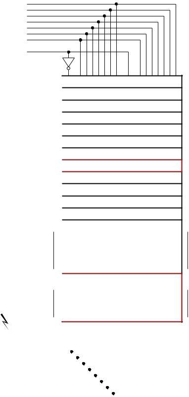
Data store
The Data store comprises 81 8-bit locations known as file registers or just files for short. The contents of any location in the Data store may be moved into or out of the Working register. The PIC16F84’s file registers are located in the Data store’s memory map as shown in Fig. 4.6. The registers can be categorised as Special-Purpose Registers (SPRs) used by the core CPU and peripheral modules for status information and controlling the desired operation of the device. The remaining implemented General-Purpose Registers (GPR) can be used by the programmer for temporary storage of program variables.
There are two ways an instruction can target a datum in the Data store. Each file register has an address, which is listed in Fig. 4.6. For example PORTA is located at File 05.
Directly
Any instruction which can process a datum in the Data store can directly specify the e ective address using seven binary bits which are part of the binary program code, the details of which are given on page 107. By itself this can address a base range of 00–7Fh. However, we see from Fig. 4.6 that this address is augmented by the RP0 bit19 in the Status register to give an e ective 8-bit address. If RP0 is 0 (as it is after reset) the range is 00–7Fh, that is Bank 0. If RP0 is made 1 then the range is 80–FFh; that is
18The older PIC16C84 uses normal EEPROM but otherwise has the same Program store architecture. However, the Data store is rather smaller.
19Actually the Data store model for the mid-range PICs is based around four 128-byte
banks with STATUS[6:5] holding two bank select bits RP1:RP0 (see Fig 5.1 on page 109) to give an e ective maximum capacity of 29 = 512 register files. Devices such as the PIC16F87X lines implement the complete model. The 8-bit file address for File Indirect memory access is augmented by bit STATUS[7], known as IRP (Indirect Register Page). This gives two 256-byte Indirect pages.
92 The Quintessential PIC Microcontroller
Direct addressing
Indirect addressing
d0
d6
RP0
File address |
|
|
|
|
|
|
|
|
|
|
|
|
|
|
|
|
|
|
|
|
00h |
|
|
|
IND |
|
|
|
IND |
||||||||||
|
01h |
|
|
TMR0 |
|
|
OPTION |
||||||||||||
|
02h |
|
|
|
PCL |
|
|
|
PCL |
||||||||||
|
03h |
|
|
STATUS |
|
|
STATUS |
||||||||||||
|
04h |
|
|
|
FSR |
|
|
|
FSR |
||||||||||
|
05h |
|
|
PORTA |
|
|
TRISA |
||||||||||||
|
06h |
|
|
PORTB |
|
|
TRISB |
||||||||||||
|
07h |
Unimplemented |
Unimplemented |
||||||||||||||||
|
|
|
|
|
|
|
|
|
|
|
|
|
|
|
|
|
|
|
|
|
08h |
|
|
EEDATA |
|
|
EECON1 |
||||||||||||
|
09h |
|
|
EEADR |
|
|
EECON2 |
||||||||||||
|
0Ah |
|
|
PCLATH |
|
|
PCLATH |
||||||||||||
|
0Bh |
|
|
INTCON |
|
|
INTCON |
||||||||||||
|
0Ch |
|
|
|
|
|
|
|
|
|
Images of the |
||||||||
|
|
68 |
|
|
|
||||||||||||||
|
|
|
|
|
68 |
|
|
|
|||||||||||
|
|
General Purpose |
|
|
|
||||||||||||||
|
|
General Purpose |
|||||||||||||||||
|
|
register files |
register files |
||||||||||||||||
|
|
|
|
|
|
|
|
|
|
|
|||||||||
|
4Fh |
|
|
|
|
|
|
|
|
|
|
|
|
|
|
|
|
|
|
|
|
|
|
|
|
|
|
|
|
|
|
|
|
|
|
|
|
|
|
|
50h |
|
|
|
|
|
|
|
|
|
|
|
|
|
|
|
|
|
|
Access |
|
Unimplemented |
Unimplemented |
||||||||||||||||
|
|
|
|
|
|
|
|
|
|
|
|
|
|
|
|
|
|
|
|
File 0 (IND) |
|
|
|
|
|
|
|
|
|
|
|
|
|
|
|
|
|
|
|
File 4 |
7Fh |
|
|
|
|
|
|
|
|
|
|
|
|
|
|
|
|
|
|
|
|
|
|
|
|
|
|
|
|
|
|
|
|
|
|
|
|
||
|
|
|
|
|
|
|
|
|
|
|
|
|
|
|
|
|
|
|
|
Register |
d0 |
|
|
|
|
|
|
|
|
|
|
|
|
|
|
|
|
|
|
|
|
|
|
|
|
|
|
|
|
|
|
|
|
|
|
|
|
|
|
Select |
|
|
|
|
|
|
|
|
|
|
|
|
|
|
|
|
|
|
|
|
|
|
|
|
|
|
|
|
|
|
|
|
|
|
|
|
|
|
|
|
|
|
|
|
|
|
|
|
|
|
|
|
|
|
|
|
|
|
|
|
|
|
|
|
|
|
|
|
|
|
|
|
|
|
|
|
|
|
|
|
|
|
|
|
|
|
|
|
|
|
|
|
|
|
|
|
|
|
|
|
|
|
|
|
|
|
|
|
|
|
|
|
|
|
|
|
|
|
|
|
|
|
|
|
|
|
|
|
|
|
|
|
|
|
|
|
|
|
|
|
|
|
|
|
|
|
|
|
|
|
|
|
|
|
|
|
|
|
|
File |
|
|
|
|
|
|
|
|
|
|
|
|
|
|
|
|
|
|
|
d7 |
|
|
|
|
|
|
|
|
|
|
|
|
|
|
|
|
|
|
|
|
|
|
|
|
|
|
|
|
|
|
|
|
|
|
|
|
|
|
|
|
|
|
|
|
|
|
|
|
|
|
|
|
|
|
|
|
|
|
|
File address
80h
81h
82h
83h
84h
85h
86h
87h
88h
89h
8Ah
8Bh
8Ch
CFh
D0h
FFh
Fig. 4.6 Data store memory map.

4. The PIC16F84 Microcontroller 93
Bank 1. For example, to set the contents of File register TRISB (File 86h) to all 1s and then to read the contents of the File register PORTB into the Working register, we need the following program:
PORTB |
equ |
06 |
; |
Register file in Bank 0 |
TRISB |
equ |
86h |
; |
Register file in Bank 1 |
STATUS |
equ |
03 |
; |
Status register |
RP0 |
equ |
5 |
; |
RP0 is bit 5 in STATUS |
; --------------------------------------------- |
|
|
|
|
|
bsf |
STATUS,RP0; |
Set RP0 to 1 -- select Bank 1 |
|
|
movlw |
0FFh |
; |
Bit pattern 11111111b |
|
movwf |
TRISB |
; |
Sent to TRISB |
|
bcf |
STATUS,RP0; |
Select Bank 0 |
|
|
movf |
PORTB,w |
; |
Read the state of PORTB |
Indirectly
If the Indirect address mode is used, as was described in Fig. 3.6 on pageref3:fig-Indirect, then the 8-bit address in the File Select Register (FSR) is used as the e ective. As we have an 8-bit address in this situation any location in the two banks are accessible with not bank switching required. The same example as described above is then implemented as:
PORTB |
equ |
06 |
; |
Register file in Bank 0 |
TRISB |
equ |
86h |
; |
Register file in Bank 1 |
STATUS |
equ |
03 |
; |
Status register |
RP0 |
equ |
5 |
; |
RP0 is bit 5 in STATUS |
; --------------------------------------------- |
|
|
|
|
|
movlw TRISB |
; |
Set up the pointer to locate TRISB |
|
|
movwf FSR |
|
|
|
|
movlw 0FFh |
; |
Bit pattern 11111111b |
|
|
movwf INDF |
; |
Sent to TRISB |
|
|
bcf |
STATUS,RP0; |
Select Bank 0 |
|
|
movf |
PORTB,w |
; |
Read the state of PORTB |
|
movlw |
PORTB |
; |
Set up the pointer to locate Port B |
|
movwf |
FSR |
|
|
|
movf |
PORTB,w |
; |
Read the state of PORTB |
|
|
|
|
|
Although there is no Bank switching required, this code segment is actually longer than the previous solution! However, Indirect addressing is useful when one location in Bank 1 requires frequent access.
The bottom 12 locations of both banks are reserved for SPRs. Although the exact location can vary across members of the mid-range family, common registers; for example, PCL and PORTA tend to have the same location. For instance, see Appendix B.
Of these, we have already met most of those involved with the core function:
INDF
The INDirect File at File 0 is not physically implemented as a register. Instructions accessing this virtual location actually put the contents of the FSR onto the Data store address bus, as described in Fig. 3.6 on page 57.

94 The Quintessential PIC Microcontroller
PCL
The Program Counter Low byte is addressed as File 2. Its relationship with the total 13-bit PC is described on Fig. 4.3.
STATUS
The Status register can be accessed in File 3. As can be seen from Fig. 4.5, this file holds the three code condition bits plus several status bits and the Data store page bit RP0.
FSR
The File Select Register at File 4 holds the indirect address used when the instruction refers to the virtual INDF address.
PCLATH
File 0Ah holds the LATch High byte for the Program Counter, as described in Fig. 4.3.
INTCON
The INTerrupt CONtrol register at File 0Bh holds the mask and status bits controlling the response of the MCU to interrupts. Its operation is described in Chapter 7. Most devices have interrupt-related bits in other registers – for example see Fig. 14.10 on page 408.
All these core SPRs are images in both memory banks.
The remaining nine SPRs relate to the configuration and control of the various peripheral interface devices. More details will be given on individual peripheral SPRs in Part 3 of the book in the appropriate chapters.
The 68 GPRs are located from File 0Ch through File 4Fh and are mirrored in Bank 1.20 Thus the instruction clrf 4Fh and clrf 0Cfh are identical and target the same physical location irrespective of the state of the Register Page bit RP0 setting. The remaining file locations are not implemented and read as 00h, as does location File 07h/File 87h – which is reserved for PORTC and TRISC in devices with 28+ pins.
Peripheral functions
Each member of the PIC family has its unique set of integrated peripheral devices. However, all PICs have parallel input/output and timer facilities. As well as these standard facilities, the PIC16F84 has a peripheral 64byte EEPROM which can be used as a small data store not dependent on continuous power to retain its contents; i.e. non-volatile.
Each of these peripheral facilities are described in detail in Part 3 of the book, but for completeness are briefly cataloged here together with their associated SPRs. These registers are used to configure the function of their target peripheral interface, to control and monitor their status.
Parallel input/output
The ability to externally alter or monitor several digital lines at the same time is a virtually universal facility on microprocessor-based systems.
20This GPR mirroring is not as a rule a feature of the more sophisticated members of the family.
4. The PIC16F84 Microcontroller 95
Apart from the 8-pin PIC12XXX series, all PICs have a minimum of 12 such external input/output lines. Some have much more, such as the 40-pin PIC16C74 which has 33 I/O lines.
The PIC16F84 has 13 I/O lines, divided up into two ports. Port A has five I/O lines mapped into the Data store address space at File 5. The remaining eight lines are allocated to Port B at File 6. These ports can be thought of as a ‘window’ into the Data store in that data written to File 5 or File 6 appear to the outside world on the corresponding pins; pins RA4…RA0 and RB7…RB0 respectively – see Fig. 10.1 on page 254. However, the electrical and logic behavior of these ports is more complex than that of a purely internal register file. This will be discussed in Chapter 11 but as an example a port bit must be configurable as either an output (so that the CPU can control the state of the associated pin) or an input (so that the CPU can read the state of this pin). To do this, each Port register has an associated Data Direction register, which Microchip call TRISA and TRISB, which map to File 85h and File 86h respectively (the term TRIS stands for TRIState – see Fig. 11.2 on page 273. These registers lie in the less convenient Bank 1 as they are usually set up at the beginning of the program and never subsequently altered.
As an example, consider that we wish to make Port B bits 6…0 an input and bit 7 an output. Then the setting up code would be:
STATUS |
equ |
03 |
; Status register is at File 03 |
RP0 |
equ |
05 |
; Bank switch bit is 5 in STATUS |
TRISB |
equ |
86h |
; Data Direction register at File 86h |
PORTB |
equ |
06 |
; Port B itself is at File 06 |
|
bsf |
STATUS,RP0 |
; Bank 1 |
|
movlw |
7Fh |
; Binary pattern 0111111 |
|
movwf |
TRISB |
; makes RB7 output, RB6...RB0 input |
|
|
|
|
As an example, subsequently pin RB7 can be pulsed high and then low as follows:
bsf |
PORTB,7 |
; Pin RB7 high (set bit 7) |
||
nop |
|
; |
Delay |
a short time |
nop |
|
; |
by putting in a few NO Operations |
|
bcf |
PORTB,70 |
|
; then |
low (clear bit 7 |
|
|
|
|
|
with the assumption that the CPU is still in Bank 0. The registers associated with parallel I/O are:
PORTA, File 05h
Only the lower five bits are implemented in this register file, feeding through to pins RA4…RA0. Pin RA4 is shared with the Timer peripheral. The upper three bits read as zero.

96 The Quintessential PIC Microcontroller
TRISA, File 85h
This is used to bitwise configure Port A bits as input or output. Setting TRISA[n] to 1 sets bit PORTA[n] as an input and to 0 as an output. Any type of reset sets the TRIS bits to 1 and the associated port bits to input.
PORTB, File 06h
A bi-directional 8-bit port connected to pins RB7…RB0. Bit RB0 doubles as a hardware interrupt input.
TRISB, File 86h
This is used to bitwise configure Port B bits as input or output. Details are the same as TRISA.
Timer
Most MCUs have facilities to either measure elapsed time and/or to generate digital on/o waveforms with well defined durations. This is normally based around one or more counters that are incremented either from an external pulse or internal clock. For instance, if an automatic packing machine needs to count cans of beans going along a conveyer belt, then a photoelectric-based transducer could act as the timer input. If a new packing carton needed to be in place every 24 cans then an internal 8-bit counter would be set to E8h (−24). When the counter overflows from FFh to 00h then an interrupt (see Chapter 7) would be generated and the MCU then take the appropriate action.
All PIC MCUs have at least a basic timer/counter known as Timer 0 (TMR0). The read/write TMR0 counter register at File 1 can be clocked from the outside world via the T0CKI (Timer 0 ClocK In) pin, which is shared with the RA4 Port A pin. Alternatively, the incrementing source can be the internal Q4 phase clock, which is one quarter of the crystal frequency. For example, for a 4 MHz crystal this is 1 MHz. Either clock source can be frequency divided by a buried 8-bit prescale counter. This divide ratio is controlled by the lower three PreScale bits of the OPTION_REG register at File 81h (see Fig. 13.2 on page 363), labelled PS2:PS1:PS0. The ratio is then 2PS+1. For example, if PS[2 : 0] = 111 then
the counter will increment at 256f , where f is the clock source frequency. The prescaler can be disconnected by setting bit 3 of OPTION_REG to 1. This will give a direct connection between pulse source and counter. Writing to the Timer 0 register also zeros the Prescaler counter (for example movlw 0F8h, movwf 1) enabling the time period to begin from true zero time.
When this PSA (Pre-Scale Assignment) bit is 1 the prescaler becomes a postscaler to the Watchdog timer – see Fig. 13.1 on page 362. The Watchdog timer is designed to reset the MCU unless periodically preset by the user’s program with the instruction clrwdt (CLeaR WatchDog Timer). This ensures that the PIC will eventually reset if due to an electrical disturbance or a software bug, the processor malfunctions, perhaps
4. The PIC16F84 Microcontroller 97
by jumping into an unprogrammed part of the Program store. This will disrupt the periodic preset. If the prescaler is assigned to the Timer then the Watchdog timer will periodically time-out (count down through zero) after approximately 18 ms.21 With PSA set to 1 then 2PS 18 ms Watchdog time-outs are required before the processor is reset. Thus, with PS[2 : 0] = 111, 27 = 128 time-outs gives a period to MCU reset of nominally 2.3 s. Thus the software must use the clrwdt instruction before this period elapses to prevent reset. This instruction also clears the Prescale counter. If it does time-out, then the TO bit in the Status register will be cleared. If desired the Watchdog timer may be disabled at the same time as code is programmed into the Program store. Various configuration bits (known as fuses) are located by the flash EEPROM programmer in location File 2007h (see Fig. 10.5 on page 261), which is not accessible during the normal run mode. Such details are normally hidden to the operator by the EEPROM programmer’s operative software.
Registers relating to Timer 0 are:
TMR0, File 1
Sometimes known as the Real-Time Clock/Counter (RTCC), is an 8-bit upcounter register that keeps tally of clock events. It may be preset to any byte value by moving data from W and read at any time. When it overflows from FFh to 00h it sets the T0IF (Timer 0 Interrupt Flag) in the INTCON (INterrupT CONtrol) register – see Fig. 7.4 on page 178. This may be used to generate an interrupt.
OPTION_REG, File 81h
Six bits in this register in Bank 1 at File 81h are used in conjunction with the timer – see Fig. 13.2 at page 363.
•PS2, PS1, PS0 at bits 2,1,0 respectively control the prescale ratio 2PS−1 for the timer or postscale ratio 2PS for the Watchdog timer.
•T0SE (Timer 0 Set Edge) at bit 4 allows the programmer to select which
edge of a pulse at the T0CKI pin will increment the counter; a 0 for / and 1 for \ .
• T0CS (Timer 0 Clock Select) at bit 5 allows the programmer to select the clock source as either the internal clock (= 0) or a transition at the
T0CKI pin.
The remaining two bits configure external interrupt edge select and electrical properties of Port B inputs.
Data EEPROM
The PIC16F84 has a block of 64 bytes of data that does not require power to retain its contents. This non-volatile memory is not part of the (volatile) Data store and is accessed through SPRs as a peripheral device. Any byte can be addressed and then read from or written to via the
21Time-out is very nominal due to process variations, 7 – 33 ms, and in addition is rather dependent on supply voltage and temperature.
98 The Quintessential PIC Microcontroller
EEDATA register as addressed by the EEADR register and controlled by the EECON1 and EECON2 control file registers. Data EEPROM has a minimum endurance of 1,000,000 writes and such data is retained for upwards of 40 years. Some typical uses of a non-volatile depository would be to hold the number of pages printed in a laser printer or total miles/kilometers travelled in a car.
Details of the Read and Write protocols are given in Chapter 15, but are briefly reviewed here for completeness.
Read
1.Put address (00 – 3Fh) into EEADR.
2.Set RD (bit 0 of EECON1) to 1 to set to the ReaD mode.
3.Read the addressed contents in EEDATA.
Write
1.Put address into EEADR.
2.Put data into EEDATA.
3.Set WREN (bit 2 of EECON1) to 1 to WRite ENable.
4.Put code 55h into EECON2.
5.Put code AAh into EECON2.
6.Begin the Write cycle by setting WR (bit 1 of EECON1) to 1.
Writing, which is normally an infrequent act, is deliberately made circuitous to protect against accidental changes to the EEPROM. The register EECON2 does not actually exist, but the interlock writing 55h followed directly by AAh to File 89h is a necessary part of unlocking the target byte. Interrupts can disrupt this sequence and should be inhibited if used. Writing takes around 50 ms to complete, and sets the EEIF (EEPROM Interrupt Flag) bit 4 of EECON1 after this time, and this can be used to interrupt the processor. The WRERR (WRite ERRor) bit 3 of EECON1 is set if a Write cycle is prematurely terminated, say, by an External reset.
Registers associated with the Data EEPROM are:
EEDATA, File 08h
This contains the addressed data after a Read action and holds data to be written into the addressed byte during a Write action.
EEADR, File 09h
The 6-bit address of the target byte is placed here before a Read or Write cycle.
EECON1, File 88h
This holds the control and status bits that:
•Trigger an EEPROM Read.
•Enable a Write action.
4. The PIC16F84 Microcontroller 99
•Trigger an EEPROM Write.
•Signals a premature end to a Write cycle.
•Signals a Write cycle has been completed. Details are given in Fig. 15.2 on page 434.
EECON2, File 89h
The EEPROM CONtrol 2 is not a physical register and reads as zero. This address is used as the target for the Write cycle unlocking sequence which is implemented by moving 55h followed directly by AAh into this virtual location.
Examples
Example 4.1
Discuss how the performance of the PIC architecture is improved by incorporating pipelining into the design of the instruction-fetch unit. Do you forsee any problems associated with handling Jump instructions (such as goto) in connection with the pipeline structure?
Solution
The pipeline is a precondition for the parallel operation of the fetch and execution units. That is, in order to allow the execution of instruction n whilst the next instruction n + 1 is being fetched from the Instruction store, internal storage must be provided to present the instruction code to the Instruction decoder. As all instructions are the same size, that is 14 bits, then the pipeline register structure and control is considerably simplified. Most conventional CISC processors have instructions that vary considerably in length. For example the 68HC11 MCU core has instructions that cover the range one through four bytes; that is the fetch phase can take between one and four bus transactions. Some more sophisticated processors have multi-stage pipelines with each stage feeding part of the execution circuitry. Thus several streams of execution activity can occur simultaneously.
The problem with pipelines is that they presuppose that the program instructions will be executed sequentially as they are stored in memory. However, instructions that disrupt this smooth running and move on the Program Counter require that the pipeline be emptied so that the instruction code of the destination travels down to the end of the pipe. For example, if instruction k is goto n, then instruction k + 1 will be in the first stage of the pipeline by the time the processor knows that the next step is actually to be instruction n. Thus a null instruction cycle needs to be executed which simply brings this instruction code into the pipeline but does not execute instruction k+1 whose code is at the end of

100 The Quintessential PIC Microcontroller
the pipeline. This is sometimes known as flushing the pipeline. Instructions such as goto need two clock cycles to execute. Conditional Skip instructions, such as incfsz and btfsc take two cycles when the skip is implemented and one otherwise. All other instructions always take one cycle.
Example 4.2
Can you determine why after a subtraction, or addition of a negative number (eg. addlw -6), the setting of the C flag is the complement of the borrow-out. Hint: Look at 2’s complement arithmetic on page 9.
Solution
The solution lies in the method of subtraction by 2’s complementing the subtrahend. The subtract instructions convert the subtrahend to their 2’s complement form and then configure the ALU to add. After the addition there can be two outcomes, depending on the relative magnitude of the minuend and subtrahend.
1.Where the subtrahend is greater than the minuend then the outcome is negative and there is no carry-out. An example of this situation is: 06 − 0A 00000110 + 11110110 = (0) 11111100 or − 4 (no carry).
2.Where the subtrahend is less than the minuend then the outcome is positive and there is a carry-out. An example of this situation is:
0A − 06 00001010 + 11111010 = (1) 00000100 or + 4 (carry).
In both cases the Carry flag acts as an inverted borrow. This is in keeping with the RISC philosophy of the PIC family, to keep the processor ‘lean and mean’. In any case this non inversion means that subtraction can be implemented by adding negative data, eg. addlw -6. This is translated by the assembler to addlw 0FCh, where FCh is of course the 2’s complement of 6.
Example 4.3
Write a program to increment a packed BCD quantity located in Data memory at File 20h.
Solution
Two Binary-Coded Decimal (BCD) digits may be packed into a single byte
to represent numbers up to 99. For example 0100 1001 File 20h represents BCD 49. Incrementing a number stored in this hybrid decimal-
binary form using the normal binary addition rules may give an incorrect result. For example 01001001 + 1 (49 + 1) gives 01001010 (4Ah) after addition, but should give 01010000 (50h). Similarly, 10011001 + 1 (99 + 1) gives 10011010 (9Ah) instead of 00000000 Carry 1 (1 00h).

4. The PIC16F84 Microcontroller 101
From these examples it can be seen that whenever any of the BCD decades equals ten after incrementation then it should be zeroed and one added to any higher decade. Based on this increment and add algorithm we can formulate the task list.
1.Increment the packed BCD byte using normal binary arithmetic.
2.IF the lower nybble of the outcome is ten then add six to the outcome.
3.IF the upper nybble of the outcome is ten then add six to it.
Program 4.1 Incrementing a packed BCD byte.
;**************************************************************
;* FUNCTION: |
Increments a BCD datum giving a BCD outcome |
* |
|||
;* ENTRY |
: |
BCD in F20h |
|
* |
|
;* |
EXIT |
: |
BCD+1 in F20h |
|
* |
;* |
EXAMPLE : |
10011000 (98) |
+ 1 = 10011001 (99) |
* |
|
;* ************************************************************
; |
|
|
|
STATUS |
equ |
3 |
; The Status register |
C |
equ |
0 |
; Carry flag is bit 0 |
DC |
equ |
1 |
; Digit Carry flag is bit 1 |
BCD |
equ |
20h |
; The BCD number is in File 20h |
; ---------------------------------------------------------- |
|||
BCD_INC |
incf |
BCD,w |
; Binary inc BCD number and put in W |
|
addlw |
6 |
; Add six |
|
btfss |
STATUS,DC |
; Needed IF produced a half carry |
|
addlw |
-6 |
; ELSE not needed |
; Now check the upper |
digit by adding 6 to |
it |
and |
checking Carry |
||
|
addlw 60h |
; Add 60h (ie six to upper digit) |
||||
|
btfss STATUS,C ; Needed |
IF caused |
a Carry |
|||
|
addlw -60h |
; ELSE cancel the correction factor |
||||
; The incremented and |
corrected BCD |
number |
is |
now |
in W |
|
|
movwf BCD |
; Put it |
out in |
memory |
|
|
END |
..... ..... |
|
|
|
|
|
|
|
|
|
|
|
|
Program 4.1 gives an e cient implementation of this task list. After incrementing using normal binary rules, six is added to the previous outcome and the DC flag checked for activity. This flag will only be set when the original nybble was ten (0Ah + 6 = 1 0h). In this case the add six operation is allowed to stand as the necessary correction otherwise it is cancelled by subtraction. The upper nybble (BCD digit) is checked and corrected in the same manner, but this time it is the full Carry flag that is tested. If this is set, then the addition of 60h is allowed to stand, otherwise it is subtracted. This Carry flag could be used to set a hundreds digit if desired, to show overflow from 99 to 100.
An alternative approach would be to subtract nine before incrementation and if the Z flag is set then leave the digit at zero and increment the higher digit; otherwise add ten. Repeat for the upper digit.
102 The Quintessential PIC Microcontroller
Example 4.4
Write a routine that will add two packed BCD numbers at File 20h and File 21h. The outcome is to be in File 22h for the hundred’s digit and File 23h for the tens and unit digits.
Solution
As in the case of Example 4.3 the binary addition of numbers that are already in BCD form may need correction afterwards. Again, a correction will be needed where the digit outcome is greater than nine. The situation is more complex in this case as the sum of two digits can be anywhere between zero and 19 (9 +9 +1(carry-in) = 19). The illegal range 10 to 19 may be determined by applying the criterion:
• Check for the range Ah to Fh (10 to 15) — for example, 3 + 9 = Ch (3 + 9 = 12).
•Otherwise check if there was a carry out to the next decade — for example, 9 + 9 = 1 2h (9 + 9 = 18).
In both cases the digit may be corrected by adding six to ‘jump over’ the six illegal BCD states.
Based on this course a possible task list is:
1.Add the two packed BCD bytes using normal binary arithmetic.
2.IF the addition results in a full Carry THEN Hundreds = 1
3.IF the addition results in a half Digit Carry OR IF the unit BCD nybble is greater than nine THEN add six to the outcome.
4.IF the last correction (if any) resulted in a full Carry OR IF the tens BCD nybble is greater than nine THEN add six to the upper nybble of the outcome.
Program 4.2 directly implements this strategy. The full Carry flag is tested three times.
1.Directly after the addition – for example, 99h + 99h = 1 32h.
2.After the first correction where six is added to the lower digit – for example, 77h + 88h = FFh; FFh + 06h = 1 05h.
3.After the second correction where six is added to the upper digit – for example, 70h + 80h = F0h; F0h + 60h = 1 40h.
If the flag is set at any point then the hundreds digit will be one; the maximum value in this case is 99 + 99 = 198.
A nybble is tested for over nine by subtracting ten. If a carry (half or full depending on which digit is being tested) is not generated then the original nybble must have been ten or greater. I have actually implemented the subtract ten operation by adding −10; that is addlw -10. This is because the sublw instruction actually takes the value in the Working register away from the literal and not the other way around – see also page 55.

4. The PIC16F84 Microcontroller 103
Program 4.2 Adding two packed BCD numbers.
;*********************************************************************
;* FUNCTION: |
Adds two |
packed |
BCD datums giving a BCD outcome |
* |
||||
;* ENTRY |
: |
BCD_1 |
in F20h, BCD_2 in F21h |
* |
||||
;* EXIT |
: |
SUM_H (hundreds digit) in F22h |
* |
|||||
;* |
EXIT |
: |
SUM_L |
(tens:units digit) |
in F23h |
* |
||
;* |
EXAMPLE : |
10011001 |
(99) + |
10011001 |
(99) = 00000001 10011000 (198) * |
|||
;* *******************************************************************
; |
|
|
|
|
BCD_1 |
equ |
20h |
; The first tens:units BCD number |
|
BCD_2 |
equ |
21h |
; The second tens:units BCD number |
|
SUM_H |
equ |
22h |
; The hundreds digit of the outcome |
|
SUM_L |
equ |
23h |
; The tens:units digits of the outcome |
|
STATUS |
equ |
03h |
; |
The Status register |
C |
equ |
0 |
; |
holding the Carry flag at bit0 |
DC |
equ |
1 |
; |
and the Digit half Carry at bit1 |
; Task 1: Add the |
two numbers using natural binary rules |
|||
BCD_ADD |
clrf |
SUM_H |
; |
Zero the hundreds digit |
|
movf |
BCD_1,w |
; |
Get the first packed BCD number |
|
addwf |
BCD_2,w |
; |
Add the second number |
|
movwf |
SUM_L |
; |
and put away as the uncorrected result |
; Task 2: Was there a full Carry from this binary addition? |
||||
|
rlf |
SUM_H,f |
; Rotate Carry into hundreds digit |
|
; Task 3: Was there a Digit half Carry from the binary addition? |
||||
|
btfsc |
STATUS,DC |
; |
IF DC=0 THEN skip |
|
goto |
ADJUST_1 |
; |
ELSE an adjustment is needed |
; or if not, is the unit BCD |
digit greater than nine? |
|||
|
addlw |
-0Ah |
; |
Take away ten |
|
btfss |
STATUS,DC |
; |
Did this give a Digit carry? |
|
goto |
TENS_CHECK ; |
IF it did THEN not >9 |
|
; ------------------------------------------------------------------- |
|
|
|
|
ADJUST_1 |
movlw |
6 |
; |
Correct the units digit by adding six |
|
addwf |
SUM_L,f |
; |
with the adjusted value back in the file |
|
btfsc |
STATUS,C |
; |
IF this gives a full Carry |
|
incf |
SUM_H,f |
; THEN record a hundreds digit |
|
; ------------------------------------------------------------------- |
|
|
|
|
; Task 4: Was there a full Carry from the previous correction (if any)?
TENS_CHECK btfsc |
SUM_H,0 |
; IF yes THEN hundreds digit will be 01h |
||
|
goto |
ADJUST_2 |
; and the tens digit will need adjustment |
|
; or IF not, is the tens BCD |
digit >9? |
|
||
|
movf |
SUM_L,w |
; Get the current partly |
corrected sum |
|
addlw |
-0A0h |
; Take away ten from the |
tens digit |
|
btfss |
STATUS,C |
; Did this give a Carry? |
|
|
goto |
FINISH |
; IF it did THEN not >9 |
|
; ------------------------------------------------------------------- |
|
|
|
|
ADJUST_2 |
movlw |
60h |
; Correct by adding 6 to |
the tens digit |
|
addwf |
SUM_L,f |
; with the adjusted value back in the file |
|
|
btfsc |
STATUS,C |
; IF this generates a Carry |
|
|
incf |
SUM_H,f |
; THEN record a hundreds |
digit |
; ------------------------------------------------------------------- |
|
|
|
|
FINISH |
.... |
..... |
|
|
|
|
|
|
|
104 The Quintessential PIC Microcontroller
Self-assessment questions
4.1The PIC16F877 mid-range MCU has a 8 kbyte Program store, which can hold up to 8192 14-bit instructions located in the range 0000 – 1FFFh. As part of a certain program, execution has to be transferred from the bottom quarter of this map to 1000h. Given that the goto instruction can only directly access 11-bit addresses (0000 – 07FFh), how could you engineer a jump to this address, i.e. goto 1000h?
4.2Write a routine to decrement a packed BCD quantity, as in Example 4.3. Hint: Devise a simple test to activate the relevant carry flag if the digit is Fh.
4.3Write a routine to add ten onto a packed BCD byte located in File 20h. Hint: This is similar to Example 4.3 but only the tens digit is augmented.
4.4Where microprocessors are used in a general-purpose computing environment, the program is normally loaded into and run from read/write RAM memory. This means that the system can run a wordprocessor one minute and a spreadsheet program the next. Of course this means of operation is not applicable to embedded applications, where the program is stored in some variety of non-volatile read-only memory. Discuss why this is so and the virtues of ROM, EPROM and EEPROM implementations of non-volatile storage.
4.5The following routine is designed to do nothing other than defer execution of the main routine by 1282 µs in a PIC MCU which is being clocked using a 4 MHz crystal. Taking into account pipelining, verify this figure.
DELAY |
clrf |
20h |
; Clear count |
D_LOOP |
incf |
20h |
; Increment |
|
decf |
20h |
; and cancel by decrementation |
|
decfsz |
20h |
; Decrement until zero |
|
goto |
D_LOOP |
|
|
.... |
..... |
|
|
|
|
|
4.6 Can you devise an algorithm and task list to subtract two packed BCD numbers located as in Example 4.4. The outcome packed byte is to be in File 23h and File 22h is to hold the overflow carry – that is the negative indicator. This overflow is to be zero if there was a full borrow out, otherwise one. For example 45h − 29h = (01)16h (that is 45 − 29 = +16) and 29h − 45h = (00)84h (29 − 45 = −84) where 84 is the ten’s complement of 16.