


272 The Quintessential PIC Microcontroller
RA4 |
|
|
|
|
|
|
|
|
|
|
|
|
Bank 0 |
|
Bank 1 |
|
|
|
|
|
|
|
|
|
|
|
|||||||
RA3 |
|
|
|
|
|
|
|
FSR |
04h |
FSR |
84h |
|||||
RA2 |
|
|
|
|
|
|
|
|
|
|
|
|
||||
|
|
|
|
|
|
|
|
|
|
|||||||
RA1 |
|
|
|
|
|
|
|
|
PORTA 05h |
TRISA |
85h |
|||||
RA0 |
|
|
|
|
|
|||||||||||
|
|
|
|
|
|
|
|
|
|
|||||||
RB7 |
|
|
|
|
|
|
|
|
|
|
|
|
PORTB 06h |
TRISB |
86h |
|
|
|
|
|
|
|
|
|
|
||||||||
|
|
|
|
|
|
|
|
|
|
|
||||||
RB6 |
|
|
|
|
|
|
|
|
|
|
|
|
|
|
|
|
RB5 |
|
|
|
|
|
|
|
|
|
|
|
Unimplemented 07h |
Unimplemented 87h |
|||
|
|
|
|
|
|
|
|
|
|
|
||||||
RB4 |
|
|
|
|
|
|
|
|
|
|
|
|
|
|
||
|
|
|
|
|
|
|
|
|
|
|
|
|
|
|||
RB3 |
|
|
|
|
|
|
|
|
|
|
|
|||||
|
|
|
|
|
|
|
|
|
|
|
||||||
RB2 |
|
|
|
|
|
|
|
|
|
|
||||||
|
|
|
|
|
|
|
|
|
|
|||||||
RB1 |
|
|
|
|
|
|
|
|
|
|||||||
|
|
|
|
|
|
|
|
|
||||||||
RB0 |
|
|
|
|
|
|
|
|
||||||||
|
|
|
|
|
|
|
|
|||||||||
|
|
|
|
|
|
|
|
|
|
|
|
|
|
|
|
|
Fig. 11.1 A boiled down view of the mid-range PIC 16CXX series Parallel Ports A and B.
Table 11.1: Summary of mid-range PIC parallel I/O provision.
Port |
Size |
Characteristics |
|
A |
5 |
I/O |
RA4 is open-drain output and common with Timer 0’s input. |
|
|
|
6 I/O in 28pin+ PICs. Shared with A/D converter. |
|
|
|
|
B |
8 |
I/O |
RB0 is shared with Hardware interrupt. |
|
|
|
RB7:4 can generate a Changed interrupt. |
|
|
|
|
C |
8 |
I/O |
28 pin+ PICs shared with Serial ports. |
D |
8 |
I/O |
40 pin+ PICs shared with parallel slave port or LCD segments. |
E |
3 |
I/O |
40 pin+ PICs shared with A/D converter. |
|
|
|
64 pin+ PIC16C9XX 8-bit Input shared with LCD segments. |
|
|
|
|
F |
8 |
Input |
68 pin+ PIC16C9XX shared with LCD segments. |
G |
8 |
Input |
68 pin+ PIC16C9XX shared with LCD segments. |
GP |
6 |
I/O |
8 pin PIC12C5XX General-Purpose I/O port. |
example the PIC16C74 shares five of the Port A lines (RA5, RA3:0) and the 3-bit Port E as analog inputs to its 8-channel A/D converter.
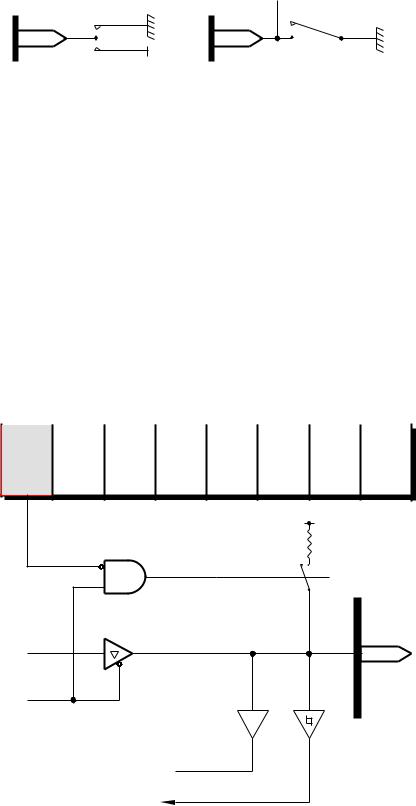
Despite the depiction of Fig. 11.1, an I/O port does not behave quite like any other internal file register. For example, it has to be configured either to read the voltages on its associated pins (input) or to be able to write to these pins (output). Furthermore, we need to determine how this configuration interferes with the action of software that tries to alter or read the state of the port.
In order to understand the characteristics of parallel I/O ports we need to look at its hardware implementation. A somewhat simplified version of a single I/O port bit n together with its associated Data Direction bit is shown in Fig. 11.2. The two key elements in this circuit are the Data D flip flop and Data tri-state (3-state) bu er.
•Writing to this port will trigger the Data D flip flop and the data on the internal Data store line will be clocked in and held as long as the MCU is powered, see Fig. 2.15(c) & (d) on page 31. For example:

 C1
C1
11. One Byte at a Time 277
fail to function as expected if that bit is set to output and pin RB7 is sinking or sourcing too much current.
(d)Writing to a port configured as an input, TRIS = 1.
In this situation the state of the Data flip flop will be altered in the proper manner. However, as the TRIS bu er is disabled, any change will not be reflected at the I/O pin until the direction of the port pin is subsequently changed to output.
This ability to set up the state of a port in a manner invisible to the outside world is important when the PIC is reset. On reset, all ports are set to input, in other words all TRIS ports are set to FFh. Any ports that are to control devices in the outside world should first be written to with the initial state of these devices and only then changed to output. For example, if four electromagnetic relays are connected to port bits RB7:4 and are to be energized after reset by logic 1 states on their input we have:
org |
0 |
; On Reset, PortB -> all inputs |
RESET movlw |
b’11110000’ |
; Set RB7:4 to 1, RB3:0 to 0 |
movwf |
PORTB |
; Do it behind the scenes |
bsf |
STATUS,RP0 |
; Change to Bank1 |
movlw |
b’00001111’ |
; Set RB7:4 to O/P, RB3:0 to I/P |
movwf |
TRISB |
; Do it exposing to outside world |
bcf |
STATUS,RP0 |
; Change back to Bank0 |
where we are assuming that the lower four Port B bits are to remain in their input state.
In item (c) we referred to current into (known as sink current) or out of (known as source current) the port pin. In most situation a port pin configured as an output will only be required to source or sink a few milliamps of drive current. Nevertheless, it is important to be aware of the drive capabilities of port output pins.
Generally two situations are tabulated in a device’s data sheet.
1.Sink current IOL when an output is logic 0 should not exceed +8.5 mA if the low voltage VOL is not to rise above 0.6 V.
2. Source current from a logic 1 output IOH should not exceed −3 mA if the high voltage is not to drop more than 0.7 V below VDD. The negative current denotes source; i.e. out of the device.
Larger currents may be sourced or sunk, as in Fig. 11.4, if degradation of logic levels are acceptable, subject to an absolute limitation that it must be within the range −20 → +25 mA for any single I/O pin to avoid damage. Where more than one I/O pin is involved in driving current, an overall global limit must be observed. For example, the 18-pin PIC16F83/4 limits Port A to −50 → +80 mA and Port B to −100 → +150 mA in total. 100 mA is the global maximum current IDD into the VDD pin and 150 mA the global maximum out of the VSS pin. Bigger packages, such as the 40-pin PIC16C74, support larger global currents with a corresponding maximum IDD of 250 mA and ISS of −300 mA.
278 The Quintessential PIC Microcontroller
The maximum current into or out of Ports A, B and E combined is 200 mA with the same figure being specified for Ports C and D in total, subject to the global IDD and ISS figures and individual pin limitation.
Port pins configured as inputs with normal TTL bu er inputs (Port A except RA4 and Port B) recognize an input as low where VIL ≤ 0.5 V and a high for an input VIH ≥ 2 V. Ports with Schmitt trigger input bu ers (RA4
and Ports C upwards) have a VIL of 0.2VDD (1 V for VDD = 5 V) and VIH of 0.8VDD (4 V for VDD = 5 V).
The block diagram of Fig. 11.1 is a typical representation of a parallel port I/O bit. Specific ports may vary in ways that can a ect the electrical performance in a significant manner; especially Ports A and B.
|
VDD |
|
|
|
|
|
|
RA0:RA3 & RA5 |
|
RA4/T0CKI |
|
|
TRP |
|
Data |
|
|
|
|
|
|
|
|
|
|
|
flip flop |
|
TRN |
Data |
|
|
TRIS |
|
VSS |
flip flop |
TRN |
|
flip flop |
|
|
|
|
|
|||
TRIS |
VSS |
|
|
|
|
flip flop |
|
To staticizer |
|||
|
|
|
|||
|
|
|
|
flip flop |
|
To staticizer |
|
|
To |
Timer 0 |
|
flip flop |
|
|
external clock input |
||
(a) Push-pull TRIS |
buffer |
|
(c) Open-drain |
TRIS buffer |
|
|
|
|
+12 V |
|
|
+12 V |
|
|
|
|
|
VDD |
|
|
1K8 |
|
|
|
|
OFF |
|
i |
|
1K8 |
|
|
|
||
i |
|
|
|
|
|
(b) Driving an electromagnetic |
relay |
(d) Driving |
an |
electromagnetic relay |
|
Fig. 11.5 Port A I/O pin driver structure.
Looking first at Port A, specifically RA3:0 and RA5, which are illustrated in Fig. 11.5(a), we see that the TRIS bu er is implemented using a series N-channel/P-channel field e ect transistor totem pole.
•Where the TRIS bit is logic 1 the lower AND gate has a logic 0 output and the upper OR gate has a logic 1 output. In this situation, both transistors TRN and TRP are non conducting and the state of the Data flip flop is isolated from the I/O pin. In this situation the port bit is configured as an input.
11. One Byte at a Time 279
• Where the TRIS bit is logic 0 then the complement state of the Data flip flop is gated through to both totem-pole transistors. With D low, TRN conducts and TRP is o giving a low pin voltage. With D high, TRP conducts and TRN is o giving a high pin voltage. In this situation the pin follows the state of the Data flip flop with current being sourced or sunk through the relatively low resistance active conducting transistors.
As an example, consider the situation where an electromagnetic relay is to be activated from pin RA0 and requires a 200 mA activation current at 12 V. For currents and voltages of this magnitude we need external bu ering. In Fig. 11.5(d) a bipolar transistor acts as an external switch. If the minimum gain of this transistor is 100 then a 1.8 kΩ resistor will give a base current of 2 mA assuming a base-emitter conduction voltage of 0.7 V and a PIC VOH of at least 4.3 V.
The output of RA4 shown in Fig. 11.5(c) is somewhat di erent in that only the bottom totem-pole transistor is implemented. As opposed to the 3-state structure of Fig. 11.5(a), this structure has only two states; that is active logic 0 and open-circuit. This type of output is known as open drain (or open-collector), see Fig. 2.3 on page 20.
• When the TRIS flip flop is logic 1, its reset state, then the AND output is low and TRN is o with the output pin high resistance. RA4 is then set to input.
•When TRIS is logic 0 the output transistor conducts when the Data flip flop is logic 0 giving an active-low output. When the Data is logic 1, TRN is o and the output floats.
An open-drain output cannot source current; either the load itself must be connected from the output pin to a positive voltage or an external pull-up resistor used as a load for the on-chip transistor. This is the case in Fig. 11.5(d) where the base current for the external transistor is derived from the 1.8 kΩ pull-up resistor when RA4 is o .
There is one further di erence between RA4 and RA0:3/RA5. The distinction is in the use of a Schmitt trigger bu er to give a better noise immunity when RA4 is used as the input to Timer 0 – see Fig. 13.3 on page 365. As a consequence, logic levels into RA4 are di erent to other Port A (and Port B) inputs. If RA4 is to be used as the Timer 0 input, it is usually configured as an input. If configured as an output, then in this situation PORTA[4] must be set to logic 1, which will disable the opendrain transistor and prevent interaction between it and the external clock input to the Timer.
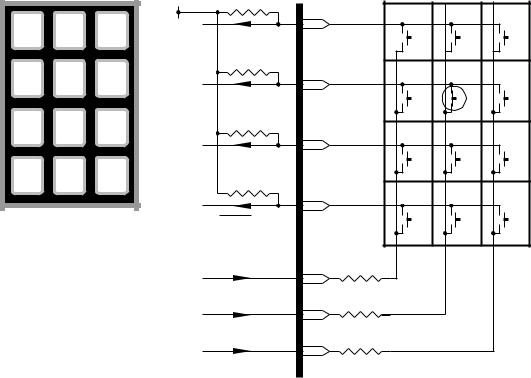
Many applications involve reading the state of arrays of switches. Rather than use the relatively more expensive single-pole double-throw (SPDT) switch arrangement of Fig. 11.6(a) to give the two logic states, most switches; for example, those in the keypad of Fig. 11.8, are single-throw (SPST) types. In these situations an external pull-up resistor is needed to
 +5V
+5V +5V
+5V
11. One Byte at a Time 281
We see from Fig. 11.7 that the internal pull-up resistors (actually a P- channel FET) are switched in only if RBPU (Register B Pull Up, bit 7) of the Option register is low. Although all eight pull-ups are qualified by RBPU only those pins configured as inputs (TRIS[n] = 1) will have the resistor switched in. RBPU resets to 1 and so the pull-up resistors default to o .
As a typical application of weak pull-ups, consider the problem of reading a keypad, such as that illustrated in Fig. 11.8(a). In this particular example there are 12 switches and rather than use up all these scarce I/O pins it is hardware e cient to connect these switches in the form of a 4×3 matrix, as illustrated in Fig. 11.8(b). This 2-dimensional array reduces the I/O pin count to 7. Larger keypads show an even greater e ciency gain, with a 64-contact 8 × 8 keyboard needing only 16 I/O pins.
1 |
2 |
3 |
VDD |
|
RB7 |
(1) |
1 |
2 |
3 |
|
|
|
|
|
|
|
|||
4 |
5 |
6 |
|
|
RB6 |
(0) |
4 |
5 |
6 |
7 |
8 |
9 |
|
|
RB5 |
(1) |
7 |
8 |
9 |
|
|
|
|
|
|||||
MEM |
0 |
SET |
|
|
RB4 |
|
|
|
|
|
|
|
|
|
(1) |
MEM |
0 |
SET |
|
(a) A 4x3 |
keypad |
|
RBPU = 0 |
|
|
|
|
|
|
|
|
|
|
|
|
|
|||
|
|
|
|
(1) |
RB3 |
330R |
|
|
|
|
|
|
|
|
|
|
|
|
|
|
|
|
|
(0) |
RB2 |
330R |
|
|
|
|
|
|
|
|
|
|
|
|
|
|
|
|
|
(1) |
RB1 |
330R |
|
|
|
|
|
|
|
|
|
|
|
|
|
|
(b) Showing |
key 5 being |
accessed |
|
|
|
|
|
|
Fig. 11.8 Interfacing to a keypad.
Although there are variations on this theme, the topology shown here is typical. The four rows are read in via RB7:4 with internal pull-up resistors enabled. The three columns connected to RB1:3 can be individually selected in turn by driving the appropriate pin low, thus scanning through the matrix. The switch contacts are normally open and, because of the pull-up resistors, read as logic 1. Should a switch connected to a low column line be closed then the appropriate row line is low. This means that
282 The Quintessential PIC Microcontroller
once the closed key row has been detected the column:row intersection is known. The 330 Ω resistors limit the current through the switch should one of the RB7:3 pins accidentally give a low output due to erroneous software.
In order to tie these concepts together, consider a subroutine to interrogate the keypad and return either with the key pressed (or at least the first key found if more than one) or if no key then −1 (i.e. FFh). Before looking at the coding we can assume that somewhere in the main software Port B has been configured appropriately with the correct input and outputs assigned and that bit RBPU in the Option register has been cleared. Something like:
include "p16f84.inc" |
|
|
MAIN bsf |
STATUS,RP0 |
; Change to Bank1 where |
movlw |
b’11110000’ |
; TRISB & OPTION_REG lie |
movwf |
TRISB |
; RB7:4 inputs, RB3:0 outputs |
bcf |
OPTION_REG,NOT_RBPU ; Activate internal pull-ups |
|
bcf |
STATUS,RP0 |
; Go back to Bank0 |
|
|
|
The listing of Program 11.1 is based on the task list:
1.Set KEY_COUNT to one.
2.For i = 0 to 2.
•Activate column i.
•For j = 0 to 3.
–Check row j.
–IF zero THEN BREAK to step 4.
–ELSE advance KEY_COUNT by 3.
•Reset KEY_COUNT back to j+1.
3.Set KEY_COUNT to −1 if no key found.
4.Return KEY_COUNT.
Basically the sequence of operations is to begin with a count of one; i.e. key[1], and bring column[0] low. As each row is checked for a zero, the count kept in the Working register is advanced by 3 (lines 21, 24, 27) to reflect the three keys in each row. If no closure (that is a 0) is found, the column key tally in memory at KEY_COUNT is advanced by one (i.e. one column) and the next column tried.
There are two ways out of the loop.
•If a 0 is found during the scan, the count in W is the desired value and the subroutine immediately returns (lines 20, 23, 26, 29).
•If the column pattern shift in line 36 results in the sample 0 arriving in bit 0 then the subroutine returns FFh to show no key has been found.
In the real world a subroutine like this would often read in rubbish due to switch bounce and possibly noise induced in the connections between keypad and the electronics.
One way of filtering out this unpredictability is shown in the subroutine of Program 11.2. Here the state of the keypad is interrogated using


|
|
|
X/Y |
|
|
|
|
[74HCT138] |
|
||
|
RA0 |
1 |
|
7 |
|
|
RA1 |
2 |
|
6 |
|
|
RA2 |
4 |
|
5 |
|
|
+5V |
|
|
4 |
|
|
|
|
3 |
|
|
|
|
|
|
|
|
|
|
& |
2 |
|
|
|
|
1 |
|
||
Fig |
RA3 |
|
EN |
|
|
|
|
|
0 |
|
|
.11 . |
|
|
|
Zone 0 |
Zone 7 |
A 10 |
|
|
|
||
|
|
|
|
[74HCT244] x 8 |
|
-multi |
|
|
|
|
|
|
|
|
|
|
|
zone |
RB7 |
|
|
|
|
RB6 |
|
|
|
|
|
intruder |
|
|
|
|
|
RB5 |
|
|
|
|
|
RB4 |
|
|
|
|
|
RB3 |
|
|
|
11 |
|
RB2 |
|
|
|
||
alarm |
|
|
|
One . |
|
RB1 |
|
|
|
||
RB0 |
|
|
|
||
|
|
|
|
||
. |
|
|
|
|
Time a at Byte |
|
[74HCT377] |
1C2 |
G1 |
2D |
|
|
|
|
|
Z7 Z6Z5Z4Z3Z2Z1Z0 |
287 |

288 The Quintessential PIC Microcontroller
when RA3 = 1. However, up to two extra output ports could be added by simply substituting RA0 by RA1 and RA2 to enable these two additional flip flop arrays. For example, one port could show which sensor(s) within the zone was active and RA4 used to sound a buzzer if any zone was active.
Program 11.3 Interacting with the intruder hardware.
; ************************************************************
; * |
FUNCTION: |
Reads Zone N |
and |
activates |
lamp N |
* |
||||
; * |
ENTRY |
: |
N is in file |
register |
ZONE, 00000nnn |
* |
||||
; |
* |
EXIT |
: |
Lamp |
N active if |
Zone |
N is |
non zero |
* |
|
; |
* |
EXIT |
: |
ZONE |
zero and TEMP unchanged |
* |
||||
; ************************************************************
ZONE_N |
bsf |
|
STATUS,RP0 |
; Change to Bank |
1 |
|
movlw |
0FFh |
; Set Port B to input |
||
|
movwf |
TRISB |
|
|
|
|
clrf |
|
TRISA |
; Set Port A to output |
|
|
bcf |
|
STATUS,RP0 |
; Change to Bank |
0 |
|
movf |
|
ZONE,w |
; Get N, used |
|
|
movwf |
PORTA |
; to select Zone |
N’s buffers |
|
|
nop |
|
|
; Delay to allow |
long lines |
|
nop |
|
|
; to settle |
|
|
movf |
|
PORTB,w |
; Now read data on Port B |
|
|
btfsc |
STATUS,Z |
; IF not zero THEN an intruder! |
||
|
goto |
LAMP_OFF |
; otherwise all clear |
||
; Intruder found, now activate lamp |
|
||||
|
bsf |
|
STATUS,RP0 |
; Change to Bank |
1 |
|
clrf |
|
TRISB |
; Port B now set |
to output |
|
bcf |
|
STATUS,RP0 |
; back to Bank 0 |
|
; Convert binary number to unary equivalent to |
activate lamp |
||||
|
movlw |
0FFh |
; All ones |
|
|
|
movwf |
TEMP |
; into TEMP |
|
|
|
bcf |
|
STATUS,C |
; Zero Carry bit |
|
|
incf |
|
ZONE,f |
; Map zone range |
to 1 -- 8 |
Z_LOOP |
rlf |
|
TEMP,f |
; Shift pattern <-- |
|
|
bsf |
|
STATUS,C |
; Set Carry bit |
|
|
decfsz |
ZONE,f |
; Decrement Zone |
number |
|
|
goto |
Z_LOOP |
; and repeat N times |
||
; TEMP holds |
the unary lamp activation pattern |
|
|||
|
movf |
|
TEMP,w |
; Get it |
|
LAMP_OUT |
bsf |
|
PORTA,3 |
; Enable output port |
|
|
movwf |
PORTB |
; Lamp data |
|
|
|
bsf |
|
PORTA,0 |
; Clock it in by |
pulsing RA0 |
|
bcf |
|
PORTA,0 |
|
|
|
return |
|
; All done |
|
|
; Go here if |
no |
intruder found and turn off all lamps |
|||
LAMP_OFF |
bsf |
|
STATUS,RP0 |
; Change to Bank |
1 |
|
clrf |
|
TRISB |
; Port B now set |
to output |
|
bcf |
|
STATUS,RP0 |
; back to Bank 0 |
|
|
movlw |
0FFh |
; All ones turns |
lamps off |
|
|
goto |
|
LAMP_OUT |
|
|
|
|
|
|
|
|
11. One Byte at a Time 289
To show how this hardware interacts with the software consider the subroutine in Program 11.3 below that reads Zone N and if non-zero then lights lamp N; where N is an integer 0–7 in a file register called ZONE on entry. We assume that an active sensor gives logic 1 and a lamp illuminates on a logic 0.
Checking Zone N is simply a matter of setting Port B up as an input port and sending the Zone N binary pattern to Port A. The 3 to 8-line decoder is enabled whenever RA3 is low, so no processing of the Zone binary code is needed. Due to the long connection lengths, a short delay is introduced to allow data to settle. For a real system, a delay of several hundreds of milliseconds and a digital smoothing routine, such as the debounce routine of Program 11.2, would be needed for reliable data acquisition, assuming that the zone bu ers were geographically distant.
Activating the eight lamps is a little more tricky. In either case, Port B must be configured as an output. The lamps are then actuated by sending the appropriate pattern to Port B, bringing RA3 high and then pulse RA0. This is implemented in Program 11.3 in routine LAMP_OUT. The lamp datum is simply all logic 1s where no intruder has been detected, that is where the sensor data has been read as all zeros.
When an intruder has been detected, then lamp N alone must be lit; for instance, 10111111b for Zone 6. To do this, the binary zone code in ZONE must be converted to the appropriate unary (one of n) code. For example, Zone 2 00000010b maps to 11111011b, Zone 3 00000011b maps to 11110111 etc.
In the program the unary code is built up in file register TEMP, which is initially set to 11111111b. By clearing Carry before entering the loop at Z_LOOP but setting it to 1 within the loop, a single zero can be shifted left using the Rotate Left File instruction rlf TEMP,f. This gives the se-
quence 11111111 ← 11111110 ← 11111101 ← 11111011 . . . 01111111. As this shift progresses, the ZONE datum (mapped to the range 1–8 so that at least one shift is implemented) is decremented and the loop exited when this reaches zero. Thus the position of the lone 0 (the initial C = 0) represents the original zone number. This unary code is then sent out to the lamp port at LAMP_OUT to activate the one-of-n indicator.
Examples
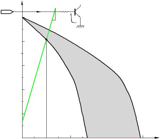
Example 11.1
A 2N3055 NPN bipolar transistor is to be used to activate the field coils of a small stepper motor. Taking into account the minimum gain of the transistor over the range +85 → −40◦C, it has been calculated that the base current must be at least 10 mA. The transistor is to be controlled from a port pin and its base-emitter voltage can be assumed to be no more than 0.7 V and VDD is 5 V. What is the maximum value of the base

11. One Byte at a Time 291
slope of the load line ∆∆VI is the resistance in kΩ (as current is in mA) and measures 280Ω.
Extending the load line onwards gives the maximum current as the X co-ordinate of the intersection with the Maximum locus, which is approximately 11.5 mA; not much di erent. If the current requirement had been larger, then the minimum/maximum currents diverge showing a significant temperature sensitivity. For example, a 20 mA minimum base current requires a base resistor of ≈ 120Ω (assuming a base voltage of 0.8 V) and the maximum base current would be 28 mA.
Example 11.2
An 18-pin mid-range PIC is to be used as a digital comparator where a parallel-input 8-bit word P is to be compared to a byte datum located in a file register named TRIP. Outputs are to indicate Lower-Than, Equivalent and Higher-Than. The comparator is to have an hysteresis of ±1 bit. That is, if previous comparisons showed N < TRIP then the trigger level is increased to TRIP +1 for equality. Similarly, on a downward trajectory the equality level is to be decreased to TRIP − 1.
Datum P is to be input via Port B set up as input and the lower three Port A pins give the active-high comparator outputs <, ==, > at RA2, RA1, RA0 respectively.
Solution
The task list for such a specification is:
1.Subtract P from LEVEL.
2.IF Equal (EQ when Z=1) THEN == output active.
3.ELSE IF P Higher than LEVEL (HI when C=0, Borrow) THEN > output active AND LEVEL = TRIP − 1.
4.ELSE IF P Lower than LEVEL (LO when C=1, No Borrow) THEN < output active AND LEVEL = TRIP + 1.
The subroutine given in Program 11.4 assumes that the main program has set up the port directions accordingly and the fixed value is in TRIP. Initially LEVEL would have been set to the same value as TRIP but would subsequently vary by ±1 as per the specification – the hysteresis band.
Software solutions to traditional hardware functions, such as comparison, have the advantage of greater flexibility, albeit at the price of a lower data throughput. Using low-cost ‘computing engines’, such as the PIC, means that relatively simple functions traditionally implemented by dedicated hardware can be replaced by embedded processors.
In this instance, flexibility could be replacing the fixed trip level by a variable datum input via, say, Port C – requiring a larger footprint device; eg. PIC16C74 (see SAQ 11.7). Example 12.1 on page 349 shows how an external datum can be serially acquired externally. Alternatively, an analog signal could represent one or both of the levels in devices with integral A/D converters – see Example 14.7 on page 428. In all these situations


11. One Byte at a Time 293
Program 11.5 Driving a stepper motor.
#define |
FREQ |
d’40’ ; |
Programmer gives value in 100k steps |
org |
050h |
; |
Code begins at 050h |
; *************************************************************
; * |
FUNCTION: |
Advances stepper motor 1 -- 256 steps |
* |
||
; * |
ENTRY |
: |
Step number in STEP |
* |
|
; * |
ENTRY |
: |
Current field position in POSITION |
* |
|
; |
* |
EXIT |
: |
POSITION updated, STEP = -1, W destroyed |
* |
; |
* |
RESOURCE: |
Subroutine PATTERN, DELAY_10MS |
* |
|
; *************************************************************
MOTOR incf |
POSITION,w |
; Advance field direction |
andlw |
b’0111’ |
; Module-8 |
movwf |
POSITION |
; updated |
call |
PATTERN |
; Get the energization pattern |
movwf |
PORTA |
; Send to stepper motor |
call |
DELAY_10MS |
; Hold off 10ms |
decfsz |
STEP,f |
; Decrement step count |
goto |
MOTOR |
; until zero |
return |
|
|
; *************************************************************
; * |
FUNCTION: |
Maps an integer 0 -- 7 to field pattern |
* |
||
; |
* |
ENTRY |
: |
Modulo-8 integer in W |
* |
; |
* |
EXIT |
: |
Stepper energization pattern in W |
* |
; *************************************************************
PATTERN addwf |
PCL,f |
; Increment Program Counter |
retlw |
b’1000’ |
; North |
retlw |
b’1100’ |
; North east |
retlw |
b’0100’ |
; East |
retlw |
b’0110’ |
; South east |
retlw |
b’0010’ |
; South |
retlw |
b’0011’ |
; South west |
retlw |
b’0001’ |
; West |
retlw |
b’1001’ |
; North west |
; *************************************************************
; * FUNCTION: |
Delays 10 ms |
delay independent of clock freq |
* |
||||||
; |
* |
ENTRY |
: |
FREQ |
is xtal |
frequency in |
multiples |
of 100kHz |
* |
; |
* |
EXIT |
: |
10ms |
delay; DELAY zero, W |
destroyed |
|
* |
|
; *************************************************************
DELAY_10MS |
|
|
|
movlw |
FREQ |
; The programmer’s statement |
|
movwf |
TEMP |
; Gives the PIC frequency |
|
; Delay loop 10ms at f = 100kHz xtal (1 cycle = 40us) |
|||
DLOOP1 movlw |
d’62’ |
; Loop count |
|
movwf |
DELAY |
|
|
DLOOP2 decf |
DELAY,f |
; 62 |
* 40us |
btfss |
STATUS,Z |
; 62 |
* 40us |
goto |
DLOOP2 |
; 62 |
* 80us |
decfsz |
TEMP,f |
; Decrement frequency parameter |
|
goto |
DLOOP1 |
; and repeat until zero |
|
return |
|
|
|
|
|
|
|
 I
I Field
Field
11. One Byte at a Time 295
header as a number FREQ in steps of multiples of 100 kHz. Thus for a 8 MHz crystal, giving a 2 MHz machine cycle, FREQ should be defined as 80 using the #define directive, before the program is assembled.
The core of the subroutine is a loop needing a nominal 10 ms execution time at a crystal frequency of 100 kHz – 40 µs machine cycle. This loop is transversed FREQ times. Thus our 8 MHz example will have a loop execution of 1080 ms but will be executed 80 times to give our required 10 ms delay.
Example 11.4
Redo the keypad driver of Program 11.1 but coded in C.
Solution
Software structures of this nature, that is interacting with peripheral devices, are classified as device drivers. Device drivers or handlers have to be able to get at individual register bits in an e cient and sometimes real-time manner. Thus, even in a software system coded in a high-level language, the device drivers are traditionally written at assembly level. However, it is possible to code most device drivers in C, especially where response time is not critical.
The essence of the use of C in interacting with the various peripheral interface devices lies in its ability to operate at the colloquially called bit twiddling (or bit banging) level. To do this the programmer must be able to access fixed addresses in the Data store and to monitor or change individual bits within a datum. We have already seen on page 242 how to directly access a known memory location. For example, the definition:
Contents of
Pointer to byte datum
In File 06
#define PORT_B *(unsigned int *)0x06
defines the name PORT_B as synonymous with the contents of File 6, that is Port B.
Any bit or bits in, say, Port B can be monitored by using the & AND operation ; for example,
if((PORT_B & 0x80) == 0) {do this;} /* Check bit7 for 0 */ if((PORT_B & 0x02) != 0) {do that;} /* Check bit1 for 1 */
executes the statement {do this;} if bit 7 is zero and {do that;} if bit 1 of Port B is a one.
Most microcontrollers have native instructions to bit twiddle single bits directly in memory in a single execution cycle. Where only one bit

296 The Quintessential PIC Microcontroller
is involved this is more e cient than the use of AND and OR operations, and because of this C compilers designed to be used for such hardware targets usually have (non standard) operators designed to make use of this feature.
On page 244 the CCS compiler #bit declaration was used to define individual bits that could subsequently be tested by code. Using this technique our example becomes:
#bit |
B7 |
= |
06.7 |
/* |
PortB, bit |
7 |
|
|
*/ |
||
#bit |
B1 |
= |
06.1 |
/* |
PortB, bit |
1 |
|
|
*/ |
||
...................... |
|
|
|
|
|
|
|
||||
if(!B7) |
{do this;} /* |
Do |
this |
if |
Bit7 is false |
(i.e. |
0) |
*/ |
|||
if(B1) |
|
{do that;} /* |
Do |
that |
is |
Bit1 is true |
(i.e. |
1) |
*/ |
||
|
|
|
|
|
|
|
|
|
|
|
|
The CCS compiler comes with a header file for each processor which includes a bit description of all that device’s Special-Purpose Register set and I/O pins. Our examples assume that we have included the file
16f84.h. Thus:
if(!input(PIN_B7)) {do this;} /* Do this if bit RB7 == 0 */ if(input(PIN_B1)) {do that;} /* Do that if bit RB1 == 1 */
There is also a complementary output function; for instance:
output_pin(PIN_B1,0); |
/* Make |
RB1 low |
*/ |
||
output_pin(PIN_B2,1); |
/* |
Make |
RB2 |
high |
*/ |
output_pin(PIN_B3,1); |
/* |
Make |
RB3 |
high |
*/ |
|
|
|
|
|
|
The CCS compiler adopts the policy that the inner workings of the various peripheral devices should be as invisible to the programmer as possible. To this end the compiler comes with a rich set of internal functions to set up and use the interface features appropriate to the target device specified by the header file.
As an example of this philosophy, set_tris_b(0xF0); is an alternative to the approach adopted on page 274. Similarly the internal function port_b_pullups(TRUE); is an alternative to setting the RBPU bit in the Option register.
The CCS compiler handles parallel I/O in several di erent ways. The #use fast_io(b) statement below leaves it up to the programmer to explicitly set up the appropriate TRIS registers. Other alternatives allow the programmer to ignore such minutia, but then the compiler will set up the port configuration each time it is used, even if that configuration remains unchanged from the last usage.
Program 11.6 assumes the following code as part of the main routine:
11. One Byte at a Time 297
#include |
<16f84.h> |
|
|
#use |
fast_io(b) |
|
|
#define PORT_B *(unsigned int *)0x06 |
|
||
unsigned int scan_it(void); |
|
||
unsigned int get_it(void); |
|
||
int main() |
|
|
|
{ |
|
|
|
int ....; |
|
/* Main’s variable declarations |
*/ |
set_tris_b(0xF0); |
/* RB7:4 outputs, RB3:0 inputs |
*/ |
|
port_b_pullups(TRUE); /* PortB pullups active |
*/ |
||
...... |
|
|
|
...... |
|
|
|
} |
|
|
|
|
|
|
|
Program 11.6 Coding the keypad device driver in C.
unsigned int get_it(void)
{
unsigned int count, old_key, new_key; count = 0;
while(count<255)
{
new_key = scan_it(); if(new_key == old_key)
{ count++;}
else
{
old_key = new_key; count = 0;
}
}
return (old_key);
}
/**************************************************************/
unsigned int scan_it(void) |
|
{ |
|
unsigned int key, pattern; |
|
key=1; pattern = 0xF7; |
/* Initial pattern 11110111b */ |
while(key<13) |
|
{ |
|
PORT_B = pattern; if(!input(PIN_B7)) {break;} if(!input(PIN_B6)) {key+=3; break;} if(!input(PIN_B5)) {key+=6; break;} if(!input(PIN_B4)) {key+=9; break;} pattern = pattern >>1;
key++;
}
if(key==13) {key = 0xff;} return key;
}

11. One Byte at a Time 299
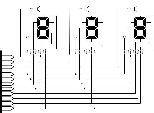
Assuming each display requires eight lines (seven segments plus decimal point) then a budget of 8 × n parallel lines are required for an n- digit display. The straightforward solution to this problem is shown in Fig. 11.13, where a 3-digit display is driven from three parallel registers on a local bus, in the manner of Fig. 11.10. The principle can be extended to six or more digits using the appropriate number of registers.
VDD |
VDD |
VDD |
|||
4K7 |
|
4K7 |
|
4K7 |
|
|
Common anode |
|
Common anode |
|
Common anode |
f |
a |
f |
a |
f |
a |
b |
b |
b |
|||
|
g |
|
g |
|
g |
e |
c |
e |
c |
e |
c |
dp |
d |
dp |
d |
dp |
d |
|
180R |
|
180R |
|
180R |
RA2
RA1
RA0
RB0
RB1
RB2
RB3
RB4
RB5
RB6
RB7
Fig. 11.14 Scanning a 3-digit 7-segment array.
The displays shown in the diagram are common anode and the appropriate LED is illuminated when the register output is low, with the sink current limited by the series resistance. In practice most logic circuitry can sink more current into a low output as compared to sourcing current from high and because of this common cathode displays are less common. In some larger displays , eg. 5 cm (2"), several LEDs may be paralleled or in series in each segment. In this situation larger anode voltages and/or currents may be needed and suitable drivers required to bu er the register outputs.
An alternative approach, shown in Fig. 11.14, is frequently used with LED-based displays. Instead of using a register for each digit, all readouts are connected in parallel to the one PIC port. Each readout is en-


 .
.
11. One Byte at a Time 301
Program 11.7 Displaying the decimal equivalent of a binary byte.
; Task 1 |
|
|
DISPLAY movf |
BINARY,w |
; Get binary byte |
call |
BIN_2_BCD |
; Convert to 3-digit BCD |
; Task 2 |
|
|
movf |
HUNDREDS,w |
; Get Hundreds nybble |
call |
SVN_SEG |
; Convert to 7-segment code |
movwf |
PORTB |
; Send out to PortB |
bsf |
PORTA,2 |
; Clock into register |
bcf |
PORTA,2 |
|
; Task 3 |
|
|
movf |
TENS,w |
; Get Tens nybble |
call |
SVN_SEG |
; Convert to 7-segment code |
movwf |
PORTB |
; Send out to PortB |
bsf |
PORTA,1 |
; Clock into register |
bcf |
PORTA,1 |
|
; Task 4 |
|
|
movf |
UNITS,w |
; Get Units nybble |
call |
SVN_SEG |
; Convert to 7-segment code |
movwf |
PORTB |
; Send out to PortB |
bsf |
PORTA,0 |
; Clock into register |
bcf |
PORTA,0 |
|
|
|
|
(a)
•Copy contents of HUNDREDS into W and convert to 7-segment code.
•Copy 7-segment code to Port B.
• Bring RA2 low \ .
•Delay 10ms.
• Bring RA2 high / .
(b)
•Copy contents of TENS into W and convert to 7-segment code.
•Copy 7-segment code to Port B.
• Bring RA1 low \ .
•Delay 10ms.
• Bring RA1 high / .
(c)
•Copy contents of UNITS into W and convert to 7-segment code.
•Copy 7-segment code to Port B.
• Bring RA0 low \ .
•Delay 10ms.
• Bring RA0 high / .
The coding in Program 11.8 makes use of the 10 ms delay subroutine illustrated in Program 11.5 to regulate the scanning rate. Apart from the length of the enabling pulse the core of the program is identical to our previous situation. However, the code must run continually to give the impression of a constant display. This illustrates the trade o between hardware and software. Reducing the hardware has lead to greater load-

11. One Byte at a Time 303
zone. An alternative approach would be to replace each zone’s 3-state bu er by a PIC. Each PIC would drive a 4-wire common bus back to the main base PIC. One wire can be used as a shared handshake line to signal the base that an intruder has been sensed at the zone indicated on the three data wires.
Show how a PIC16F84 could be configured as a Zone PIC paying particular attention to the usage of the single handshake line shared with all zones.
Would it be possible to reduce the number of wires to three? How could a local display be added to show which sensor has been set o ?
11.2 A certain PIC running at 20 MHz has its Port C connected to LEDs tied high through a 1 kΩ resistor and with a 300 pF capacitance to ground. All LEDs are o and the programmer attempts to turn on LED 7 and LED 0 as follows:
bcf |
PORTC,7 |
; |
Turn |
on |
LED7 |
bcf |
PORTC,0 |
; |
Turn |
on |
LED0 |
|
|
|
|
|
|
However, only LED 0 actually turns on. What is happening?
11.3A certain system needs to be able to both activate eight LEDs and to be able to read the state of up to eight normally-open (N.O.) push switches. It has been proposed that a single Port B might be able to combine these functions – the former when set to output, the latter when set to input. Can you devise a suitable circuit?
11.4A PIC-based reaction meter is to be designed to act as a crude bloodalcohol level indicator. The principle of the device is that a buzzer is sounded for 100 ms when the unseen tester closes his or her switch. The subject is to respond to the sound by immediately pressing his/her switch. An 8-LED barograph display is to indicate the passage of time by progressively illuminating an additional LED every 50 ms. The number of lit LEDs at the conclusion of the test is the reaction time in 50 ms steps.
Show how a PIC16F84 could be configured in hardware and software to read both switches and activate the eight LEDs and one buzzer.
11.5 The variation of logic 0 output voltage VOL against sink current IOL for the two extremes of the commercial temperature range is shown in Fig. 11.15. Using this graphical relationship determine the maximum value of series resistor to ensure a current of no less than 20 mA will

304 The Quintessential PIC Microcontroller
flow through an LED connected to +5 V, as shown in the diagram, for any temperature. With this value what will be the current be at −40◦C? You can assume that the conducting voltage across the LED is a constant 2 V.
|
|
|
+5 V |
VOL |
IOL |
RB |
|
5 V |
|
|
|
4 V |
|
|
|
3 V |
|
|
|
2 V |
|
|
|
|
Min @ +85 C |
Max @ -40 C |
|
1 V |
|
|
|
0 |
20 |
40 |
60 |
80 |
100 |
IOL (mA) |
|
Sink
Fig. 11.15 Low-level output voltage against sink current.
11.6Repeat the exercise of SAQ 11.4 but coding in C.
11.7Extend the digital comparator of Example 11.2 to compare two external digital bytes presented to a 28-pin footprint PIC, with byte P being input at Port B and Q at Port C.
11.8In a low-power wireless data logging system placing the PIC in its sleep mode will not a ect the current consumption of the radio transmitter. It is proposed to use a port pin to supply current to the transmitter and in way this auxillary circuitry can be switched on and o as necessary. Discuss.