CHAPTER 12
One Bit at a Time
Parallel data transmission is fast, with a minimum of software overhead. However, there are circumstances where its use is inappropriate; either because of the additional hardware cost (see Fig. 11.10 on page 287) or more commonly where the receivers are geographically distant, with the concomitant cost or non availability of multiple communication channels and their necessary interface hardware. In such situations data can be sent one bit at a time and assembled by the remote device into the original data bytes. In this manner a comparison can be made with the parallel port on a PC, commonly used for local peripherals, such as a printer, and the serial port frequently used with a modem to link into the internet via a single telephone line.
|
Smart bank |
|
|
.com |
|
|
|
VISA |
+5V |
|
|
RST |
|
|
CLK |
Serial I/O |
Hologram |
|
|
Embossing area |
DEBIT |
|
CARD |
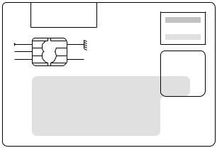
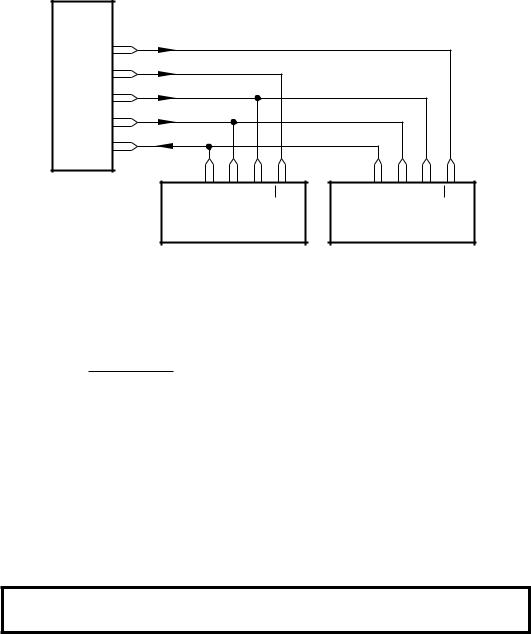
Fig. 12.1 The smart card.
As an example, consider the smart cards in your wallet. Each card will have an embedded microcontroller, typically 8-bit, giving it its intelligence. Cost constraints are severe to give a manufacturing price of under $1, and a large component of this is accounted by the non corrosive gold-plated contacts via which the microcontroller is powered and clocked when in contact with the card reader. In order to keep the mechanical precision of the reader low and hence reliability high, the number of contacts must be minimized and pad size maximized.

12. One Bit at a Time 307
dp |
dp |
dp |
|
|
330R |
|
|
330R |
|
|
330R |
SRG8 [74HCT164] R |
C1/ |
& 1D |
SRG8 [74HCT164] R |
C1/ |
& 1D |
SRG8 [74HCT164] R |
C1/ |
& 1D |
VDD |
|
|
VDD |
|
|
VDD |
|
|
SCK
RA1
RA0 SDO
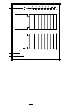
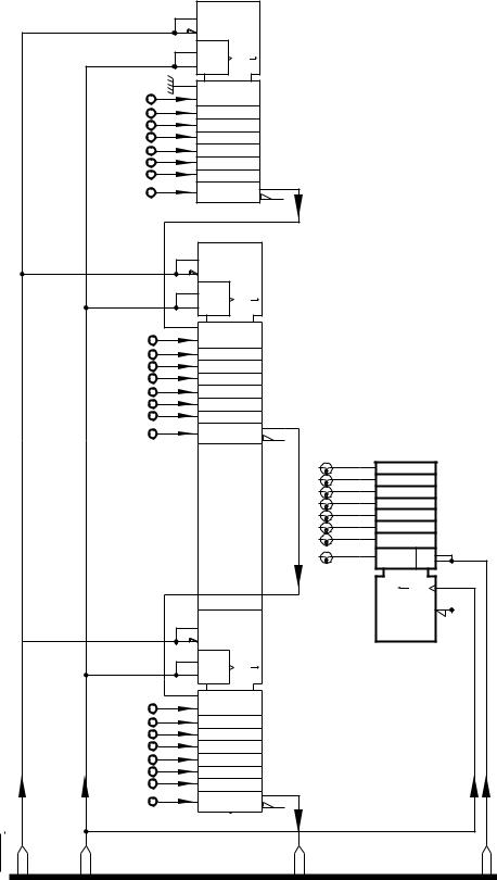
Fig. 12.2 Serial interface to a 3-digit 7-segment display.
driver routine of Program 11.7 on page 301 which converts a binary byte to an array of BCD digits in HUNDREDS, TENS and UNITS. These are mapped to 7-segment code and then sent out to each digit 8-bits at a time.
To serialize this process we require to design a subroutine to put each bit of a specified file register DATA_OUT out at SDO while pulsing SCK, beginning with the leftmost bit. A task list for such a subroutine is:
1.Bring SCK low.
2.COUNT = 8.
3.WHILE COUNT > 0 DO:
(a)Shift DATA_OUT left into Carry.
(b)Copy Carry to SDO.
(c) Pulse SCK / \ .
(d) Decrement COUNT.
Program 12.1 shows two subroutines. The first called DISPLAY is closely akin to Program 11.7 in that it calls the subroutines BIN_2_BCD and then sends the 7-segment coded bytes out to the interface registers. In this instance the units byte is sent first as this will eventually be shifted to the far end of the chain; followed by the tens and finally the hundreds byte.
The actual serial transmission is handled by the subroutine SPI_WRITE, which implements our task list. The datum placed by the caller in file register DATA_OUT is shifted left and the state of the Carry bit used to make the Serial Data Out pin RA0 0 or 1. The Serial ClocK pin RA1 is then toggled once / \ to shift the data into the shift register chain. This is repeated eight times to complete the transaction, which takes a maxi-

12. One Bit at a Time 309
Where a long chain of shift registers is being serviced, speed may be improved a little if each register has its own data feed but all clocked with the same SCK pin or sharing the same lines but each with a separate Enable. This latter technique is the method used in Fig. 12.8.
One problem with our shift register technique is that for the period where shifting is in process the data appearing at the port outputs are not valid; for 23 clock pulses in our example. Of course in this situation the response of the eye to microsecond changes in illumination makes this observation spurious. However, this may not always be the case and in such instances the shift register may be bu ered from the parallel outputs using an array of D flip flops or latches, which can be loaded after the shifting process has been completed to give a single update.
|
|
A B C D E F G H |
G |
EN3 |
|
|
|
|
|
C2 |
2D |
RCK |
|
SOUT |
|
SRG8 R C1/ |
1D |
SCLR |
|
|
SCK |
|
|
|
|
SIN |
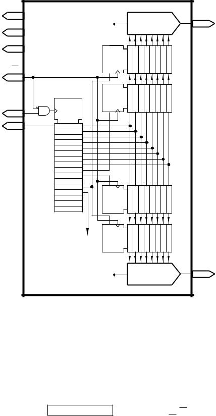
Fig. 12.3 Logic functional diagram of the 74HCT595 octal shift register with output register.
Rather than employing a separate bu er register, a more e cient solution typically uses the 74HCT595 of Fig. 12.3 with its integral 8-bit parallel-in parallel-out (PIPO) register between the shift register and the outside world. A rising edge / on the RCK (Register ClocK) pin transfers the serialized data to the parallel outputs. The last stage output of the shift register is made available to allow cascading to any length. All RCK pins can be pulsed together to allow the entire chain to simultaneously update.
One example where rippling of data may be undesirable, is were a digital datum is to be converted to its analog equivalent. In Fig. 12.4 the conversion is carried out using a National Semiconductor DAC0800. Essentially the analog voltage is a linear function of the 8-bit digital input

312 The Quintessential PIC Microcontroller
datum should be continually presented to SDO at at the same time as it is read in at SDI or a latched register, such as the 74HCT595, used to staticize the display data. As an alternative, separate serial clock lines could be used.
The core serial interface software is the input counterpart of subroutine SPI_WRITE in Program 12.1, which implements the following task list:
1.Bring SCK low.
2.COUNT = 8.
3.WHILE COUNT>0 DO:
(a) Pulse SCK / \ .
(b)Copy input SDI to Carry.
(c)Shift left Carry into DATA_IN.
(d)Decrement COUNT.
This task list is similar to that for subroutine SPI_WRITE except that the Carry bit is shifted into the file register, its value depending on the state of the SDI pin following the clock pulse. After eight clock-shift-test loops the datum in DATA_IN is the parallelized byte assembled from the serial input port, with the first bit ending up in the leftmost significant placeholder in DATA_IN.
Program 12.2 Input serial byte subroutine.
; *****************************************************
; * |
FUNCTION: |
Clocks in a byte in series, MSB first |
* |
||
; |
* |
ENTRY |
: |
None |
* |
; |
* |
EXIT |
: |
Datum in DATA_IN; COUNT = 0 |
* |
;*****************************************************
;Task 1: Bring SCK low
SPI_READ |
|
|
|
|
bcf |
PORTA,SCK |
; |
Make sure clock |
starts at low |
; Task 2: COUNT=8 |
|
|
|
|
movlw |
8 |
; |
Initialize loop |
counter to 8 |
movwf |
COUNT |
|
|
|
;Task 3: WHILE COUNT>0 DO:
;Task 3 (a): Pulse SCK SER_IN_LOOP
bsf |
PORTA,SCK |
|
bcf |
PORTA,SCK |
|
; Task 3(b): Copy input |
SDI to Carry |
|
bcf |
STATUS,C |
; Zero Carry |
btfsc |
PORTA,SDI |
; Check data input |
bsf |
STATUS,C |
; IF 1 THEN set Carry |
; Task 3(c): Shift data |
bit in (Carry) |
|
rlf |
DATA_IN,f |
; Shift data bit in (Carry) |
; Task 3(d): Decrement |
COUNT and repeat |
Task3 |
WHILE>0 |
|||
decfsz |
COUNT,f |
|
; |
Decrement |
count |
|
goto |
SER_IN_LOOP |
; |
and repeat until zero |
|||
return |
|
|
|
|
|
|
|
|
|
|
|
|
|

314 The Quintessential PIC Microcontroller |
|
|
|||
VDD |
|
|
|
|
|
8 |
[MAX549A] |
Vref |
|
DACA |
VoutA |
Vref |
|
2 |
|||
6 |
|
|
|
|
|
GND |
|
G1 |
1C2 |
2D |
DACREGA |
CE |
|
||||
1 |
|
|
|
|
|
3 |
|
|
|
|
INREGA |
SCLK |
SRG16 |
G1 |
1C2 |
2D |
|
|
|
|
|
|
|
5 |
C1 |
|
|
|
|
|
|
|
|
|
|
4 |
D1 |
|
|
|
|
DIN |
|
|
|
|
|
|
A0 |
|
|
|
|
|
A1 |
|
|
|
|
|
X |
|
|
|
|
|
C1 |
G1 |
1C2 |
2D |
INREGB |
|
C2 |
||||
|
|
|
|
|
|
|
X |
|
|
|
|
|
X |
|
|
|
|
|
X |
|
|
|
|
|
Power |
G1 |
1C2 |
2D |
DACREGB |
|
down |
|
|
|
|
|
|
Vref |
|
DACB |
VoutB |
|
|
|
7 |
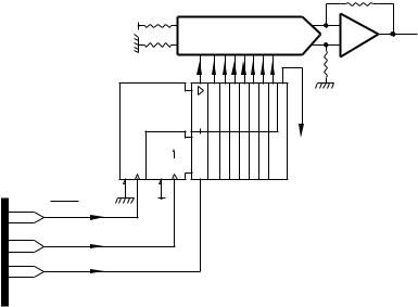
||
Fig. 12.6 The MAX549A SPI dual 8-bit DAC.
be stored but will not appear at the input of the DAC until the next layer PIPO register is clocked. This register is enabled when C1 is 1 and CE is pulsed. This means that one data byte can be sent to, say, DACA and then another to DACB. The DAC registers can then be updated together, resulting in both outputs VoutA and VoutB changing simultaneously; see Program 12.3. This can even be done when the MAX549A is asleep, as the registers are not a ected by this power-down state.
From this discussion we see that each transition from the PIC takes two 8-bit transfers Control  Data followed by a / on the CE pin. For our example we will send the contents of File 20h to Channel A and then the contents of File 21h to Channel B, at that point updating both

12. One Bit at a Time 315
DAC registers and hence outputting the analog equivalent of File 20h to
pin VoutA and File 21h to pin VoutB. We assume that both AD0 and AD1 pins are connected to Ground.
Our implementation will involve the transmission of four bytes of information:
1.Control byte 1: XXX00X01
No power down, update Channel A, no output change.
2.Data byte 1: Contents of File 20h.
3.Control byte 2: XXX01X10
No power down, update Channel B, both outputs change.
4.Data byte 2: Contents of File 21h.
The hardware-software interaction is shown in Program 12.3. Four bytes are transmitted using subroutine SPI_WRITE, with the MAX549A’s
CE being pulsed / \ after each Control  Data byte pair. The final
|
Program 12.3 Interacting with the MAX549A dual-channel SPI DAC. |
|
|
|
include "p16f84.inc" |
CE |
equ 2 |
;**********************************************************
;* FUNCTION: Sends out Channel A & B data to SPI protocol *
; * FUNCTION: |
MAX549A simultaneously updating |
outputs |
* |
|||
; * RESOURCE: |
Subroutine SPI_WRITE |
|
* |
|||
; |
* |
ENTRY |
: |
Channel A in File20h, Channel B |
in File21h |
* |
; |
* |
EXIT |
: |
Both analog outputs updated |
|
* |
; **********************************************************
movlw |
b’00000001’ |
; Control byte 1 |
movwf |
DATA_OUT |
; Put in designated location |
call |
SPI_WRITE |
; and send out to MAX549A |
movf |
20h,w |
; Get Channel A data |
movwf |
DATA_OUT |
; Put in designated location |
call |
SPI_WRITE |
; and send out to MAX549A |
bsf |
PORTA,CE |
; Pulse CE |
bcf |
PORTA,CE |
|
movlw |
b’00001010’ |
; Control byte 2 |
movwf |
DATA_OUT |
; Put in designated location |
call |
SPI_WRITE |
; and send out to MAX549A |
movf |
21h,w |
; Get Channel B data |
movwf |
DATA_OUT |
; Put in designated location |
call |
SPI_WRITE |
; and send out to MAX549A |
bsf |
PORTA,CE |
; Pulse CE |
bcf |
PORTA,CE |
|
return |
|
|
|
|
|

 Data
Data
 , idle low
 , idle high
12. One Bit at a Time 319
Figure 12.10 shows the SSP CONtrol register at File 14h and the associated SSPSTATus register in Bank 1 at File 94h. The SSP port is enabled for whatever protocol when SSPEN (SSP ENable) in SSPCON[5] is 1. As SSPEN resets to zero, the SSP is disabled by default. In the disabled state the relevant Port C pins can be used as normal parallel I/O lines. If they are to be used as SSP lines then RC5:3 must be set via TRISC to be input or output as appropriate to their SSP function. Similarly, if the SS control is to be used, RA5 must be set to input.
Bits SSPCON[3:0] are the Mode control bits which set the communication protocol and various Master/Slave options as listed in Table 12.1. Of interest to us is the internal clock source in the SPI Master mode and the use of the SS pin when in the SPI Slave mode.
Finally, SSPCON[7] is the Write COLlision (WCOL) status bit – not in SSPSTAT due to lack of space. This is set to 1 if the software writes to SSPBUF before the transmission of the previous byte has been completed. If set, it should be cleared by software to reset this warning mechanism.
Using Figs. 12.9 and 12.10 as a programmer’s model we can now deduce the hardware-software interaction in order to action a transmission of a byte and/or receive a new byte:
1.Configure SSP module.
•Set up SCK/RC3, SDO/RC5 as outputs and SDI/RC4 as an input (TRISC[5:3])
•Set up Master/Slave mode with appropriate clock source (SSPCON[3:0])
•Choose active TX clock edge with CKP (SSPCON[4])
•Enable the SSP by setting SSPEN (SSPCON[5])
2.Move datum to SSPBUF to initiate transmission.
3.IF WCOL = 1 THEN reset WCOL and go to item 2
4.Poll BF for 1 (SSPSTAT[0])
5.Move RX data from SSPBUF, which also resets BF
To illustrate this process, consider a subroutine SPI_IN_OUT which combines the function of SPI_READ and SPI_WRITE; that is it transmits the datum in file register DATA_OUT whilst at the same time returning the consequential received byte to DATA_IN.
Table 12.1: The SSP Mode bits.
SSPM[3:0]: Synchronous Port Mode select bits
0000 SPI Master mode with SCK = Fosc/4 0001 SPI Master mode with SCK = Fosc/16 0010 SPI Master mode with SCK = Fosc/64
0011 SPI Master mode with SCK = TMR2 output/2
0100 SPI Slave mode. SS pin control enabled
0101 SPI Slave mode. SS pin control disabled 0110 I2C Slave mode, 7-bit address
0111 I2C Slave mode, 10-bit address
1011 I2C Start & Stop bit interrupts enabled, Slave idle
1110 I2C Slave mode, 7-bit address with Start & Stop interrupts enabled 1111 I2C Slave mode, 10-bit address with Start & Stop interrupts enabled

320 The Quintessential PIC Microcontroller
The implementation of this subroutine depends on setting up the SSP during the initialization phase of the main software after Reset. In the following code fragment we are using the Fosc/4 clock rate Master mode:
.include "p16c74.inc" |
|
||
MAIN bsf |
STATUS,RP0 |
; Change to Bank |
1 |
movlw |
b’11010111’ |
; RC5/SDO, RC3/SCK outputs |
|
movwf TRISC |
; RC4/SDI input |
|
|
..... ..... |
|
|
|
bcf |
STATUS,RP0 |
; Return to Bank |
0 |
movlw |
b’00100000’ |
; Enable SSP, TX |
clock on -ve edge |
movwf |
SSPCON |
; SPI Master, Fosc/4 rate |
|
|
|
|
|
The coding shown in Program 12.4 follows the task list exactly. Data to be transmitted is moved from the designated file register to SSPBUF and status bit WCOL checked to see that it got there. If there was a transmission in progress then the datum is not stored in SSPBUF and WCOL is set. If this subroutine is the only code to access the SSP then this should rarely be the case and in most instances this check is omitted, but its inclusion makes the system more robust.
Once the transmit datum is in situ, the transmit sequence is immediately initiated, as shown in Fig. 12.11 and progresses to its conclusion. Once the Bu er Full status flag BF is set, the received datum can be moved out of SSPBUF to its ordained location. This automatically resets BF.
Program 12.4 Using the SSP for SPI data input and output.
;************************************************************
;* FUNCTION: Transmits and simultaneously receives one byte *
; * |
FUNCTION: |
from the SSP using the |
SPI protocol |
* |
|||
; |
* |
ENTRY |
: |
Data |
to be transmitted |
is in DATA_OUT |
* |
; |
* |
EXIT |
: |
Data |
received is in DATA_IN |
* |
|
; ************************************************************
SPI_IN_OUT |
|
|
movf |
DATA_OUT,w |
; Get datum for transmission |
movwf |
SSPBUF |
; Put into SSPBUF |
SSP_IN_OUT_LOOP |
|
|
btfss |
SSPCON,WCOL |
; Did it make it? |
goto |
SPI_IN_OUT_CONT |
; IF so THEN continue |
bcf |
SSPCON,WCOL |
; ELSE reset WCOL and try again |
goto |
SSP_IN_OUT_LOOP |
|
SPI_IN_OUT_CONT |
|
|
bsf |
STATUS,RP0 |
; Change to Bank0 |
btfss |
SSPSTAT,BF |
; Check for Buffer Full |
goto |
SPI_IN_OUT_CONT |
; IF not then poll again |
bcf |
STATUS,RP0 |
; Back to Bank 1 |
movf |
SSPBUF,w |
; ELSE get the received datum |
movwf |
DATA_IN |
; Put away |
return |
|
|
|
|
|

12. One Bit at a Time 323
To illustrate this technique, consider our interface to the MAX549A coded in Program 12.3. In order to do this the SSP needs to be configured using code of the form:
#include <16c74.h> |
|
|
|
|
|
#bit |
CE = 5.2 |
/* |
Port |
A, bit 2 to MAX549A’s CE |
*/ |
void |
MAX549A(unsigned int |
channel_A, unsigned int channel_B); |
|||
set_tris_a(0xFB); |
/* |
CE = |
RA2 output |
*/ |
|
setup_spi(spi_master|spi_l_to_h|spi_clk_div_4); |
|
||||
|
|
|
|
|
|
has already been executed.
The MAX549A’s CS is connected to Port A’s RA2 pin, and is identified in the setup code using the #bit directive, as described on page 244. With this definition in mind, the code in Program 12.5 simply comprises
four spi_write() calls with CE being pulsed between Control 
 Data pairs. The function may be called with an evocation something like
MAX549A(data_x, data_y);
Program 12.5 Interfacing to the MAX549A in C.
void MAX549A(unsigned int channel_A, unsigned int channel_B) |
|
|
{ |
|
|
spi_write(0x01); |
/* Send out Control 1 |
*/ |
spi_write(channel_A); |
/* Send out Data 1 |
*/ |
CE=0; |
/* Pulse CE |
*/ |
CE=1; |
|
|
spi_write(0x0A); |
/* Send out Control 2 |
*/ |
spi_write(channel_B); |
/* Send out Data 2 |
*/ |
CE=0; |
/* Pulse CE |
*/ |
CE=1; |
|
|
} |
|
|
|
|
|
The key CCS compiler internal functions used for the SSPort in its SPI mode are:
setup_spi(spi_master|spi_h_to_l|spi_clk_div_4);
This function configures the SSP as an SPI Master, with clock polarity rising edge and a ÷4 clock frequency. These scripts, and others such as spi_slave are part of the included header file 16c74.h. This function also sets the direction of the appropriate Port A and Port C pins.
spi_write(value);
Used to write out the value from the SSP. Checks that the BF flag is set before returning.
spi_read();
Virtually identical to spi_write() except that it returns the value read by the SSP. If a value is passed to this function then it will be clocked out of SDO.

|
12. One Bit at a Time |
325 |
Start |
Acknowledge receiver from |
Idle Stop |
SCL |
1 |
2 |
3 |
4 |
|
5 |
6 |
7 |
8 |
9 |
SDA |
|
|
|
|
|
|
|
|
|
|
|
|
|
|
Eight |
Data |
bits |
|
|
|
|
Fig. 12.13 Data transfer on the I2C bus.
be clocked into the slave on the following SCL rising edge. This data may represent address, control or information bits.
At the end of the byte transfer, the Slave pulls SDA low to tell the Master that the data byte has been received. To allow this to happen the Master must release its control over SDA by allowing it to be pulled high via the bus resistor. Should the Slave not Acknowledge the transfer then the Master should abort the transfer and usually try again until timed out.
Several byte transfers will occur before the Master completes the transmission by bringing SDA high when the Clock is high. This Stop condition terminates the conversation. Another one can be initiated during the subsequent Idle state when the Master again sends out a Start bit. A Slave can distinguish the special Start and Stop situations, as this is the only time SDA changes when SCL is high.
The data transmission is framed between Start and Stop pairs and data flow can either be Master-Write as described or from Slave to Master in Master-Read mode. In the latter case it is the Master that acknowledges each byte. If it does not (No ACKnowledge or NACK) then the Slave knows that the Master has finished and floats its SDA pin allowing the Master to output a Stop bit and then Idle both lines – see Fig. 12.23(b). It is possible for the Master to begin by writing data to the Slave and then request a change of direction. In this case a second Start bit is sent by the Master without stopping, followed by the appropriate control bits.
In using a PIC MCU to implement the I2C standard a problem arises as port outputs are not open-drain; that is the logic 1 output state is not open-circuit as required in Fig. 12.14(a). However, it is possible to get around this, simulating the high impedance state by switching the port line output to input. For example, if we wish to use RA2 as the SCL data line then to pulse SCL low and then high we have:
|
|
|
12. One Bit at a Time |
327 |
Start |
Ack |
Ack |
Ack |
Stop |
Slave address byte |
|
Command/Control byte |
Data byte |
SDA |
SCL
Fig. 12.15 A I2C packet transmission.
ufacturer of the I2C peripheral and is factory programmed. To allow more than one device of the same kind to share the same bus, most I2C- compatible devices allow two to four bits of this address to be set locally by the designer, usually by connecting Slave address pins to the appropriate logic levels. On receipt of a Start bit, all Slaves on the bus will examine the first seven bits for their personal address. If there is no match then the rest of the conversation is ignored until the next Start bit. Bit 8 is a direction bit, R/W is low if the Master is to be the transmitter and high if the Slave is to be the transmitter.
Not all 7-bit addresses are valid. All addresses matching 0000XXXb or 1111XXXb are reserved for special situations, leaving 224 valid addresses in total. Along with the introduction of a Fast mode, the I2C protocol was extended to permit a 10-bit address. This is signalled by the reserved address 11110XXb. In this case a second address byte is sent with the two XX bits in the first byte making up the total 10-bit Slave address.
After the address byte(s), the next byte is usually treated by the addressed Slave as a Command/Control word, passing configuration information. For example a I2C memory may require the internal address where the data is to be written to – see Example 12.3. Bytes following this are usually pure data or a mixture of data and control bytes.
In order to illustrate these concepts we will use the Maxim MAX518 DAC, shown in Fig. 12.16, as our exemplar. This is the I2C counterpart to the SPI protocol MAX549, with a 2-layer register pipeline, two channels and a power-down feature.
The MAX518 has a 7-bit Slave address of the form 01011AD1AD0 where AD1 and AD0 are the logic state of pins 5 and 6 respectively. If we assume that both pins are connected to GND then the Address byte sent out by the Master will be 01011 
 00
00 
 0 with R/W being 0, as this device can only be written to.
The Command byte is of the form 000 RST PD XX A0 with three active control bits:
A0
Enables the input PIPO register for Channel 0 if 0 and Channel 1 if 1.
PD
When 1 will power down both DAC channels, reducing the supply current to typically 4 µA. The contents of the internal registers remain unchanged
328 The Quintessential PIC Microcontroller
|
|
|
|
[MAX518] |
|
|
Vout0 |
SDA |
|
|
|
|
|
DAC0 |
|
|
|
Start/stop detector |
|
|
1 |
||
4 |
|
|
|
|
|
|
|
3 |
|
|
|
|
|
INREG0 DACREG0 |
|
SCL |
|
|
|
|
|
||
SRG8 |
C1 |
D1 |
C1 C1 |
1D 1D |
|
||
GND |
|
|
|
|
|
|
|
2 |
|
|
|
|
|
|
|
VDD |
|
|
|
|
|
|
|
7 |
|
|
|
|
|
|
|
|
|
|
|
C1 |
1D |
|
INREG1 |
AD0 |
|
|
|
C1 |
1D |
|
DACREG1 |
6 |
|
|
Decoder/ |
|
|
|
|
AD1 |
|
|
|
|
|
Vout1 |
|
|
Address comparator |
|
|
DAC1 |
|||
5 |
|
|
|
|
|
8 |
|
Fig. 12.16 The MAXIM MAX518 I2C dual digital to analog converter.
and data may be shifted in and registers updated in this condition. The state information is only executed whenever a Stop condition is sent by the Master, when the last transmitted value of PD is acted upon.
RST
All internal registers are cleared irrespective of the following data byte which may be treated as a dummy byte. Analog outputs go to zero after the Stop condition.

330 The Quintessential PIC Microcontroller
bus runs and few Slave devices this value of resistance can be increased by up to a factor of ten to reduce energy dissipation when an output pin is low.
In implementing the I2C timings, a PIC with a crystal above 3.2 MHz, with an execution time of less than 1.25 µs, may need to insert short delays between actions. For example, a 20 MHz crystal driven PIC implementing the instruction pair:
|
bcf |
TRISA,SCL |
; |
Drag Clock low by making pin an output to logic 0 |
|
|
bsf |
TRISA,SCL |
; |
Float clock high by making pin an input |
|
|
|
|
would give high and low durations of only 0.2 µs. Short delays are conveniently implemented using nop (No OPeration) instructions; each taking one instruction cycle (Fosc/4). For example, to give a nominally 400 kHz clock at 20 MHz we have:
bcf |
PORTA,SCL |
; Clock low |
nop |
|
; 0.2us |
nop |
|
; 0.4us |
nop |
|
; 0.6us |
nop |
|
; 0.82us |
nop |
|
; 1.0us |
nop |
|
; 1.2us |
bsf |
PORTA,SCL |
; Clock high |
nop |
|
; 1.6us |
nop |
|
; 1.8us |
nop |
|
; 2.0us |
nop |
|
; 2.2us |
nop |
|
; 2.4us |
nop |
|
; 2.6us |
|
|
|
Of course slower clock speeds require less nops but rather than tailor our subroutines for one particular crystal we will use the assembler macro called Delay_600, coded in Program 12.6, that will expand to the appropriate number of nops to give a nominal 600 ns (0.6 µs) delay, depending on the value of the constant XTAL defined by the programmer at the head of the source file.
For example to alter the coding of Program 12.7 to suit a 12 MHz crystal system then the one line #define XTAL 20 should be altered to #define XTAL 12 and the program reassembled.
The coding of Program 12.6 makes use of the conditional assembly directive if – endif. This is similar to the C language statement if(true){do this;} of page 249 in that all instructions down to the following endif are implemented if the argument of the if directive is true. For example, if((XTAL>6)&&(XTAL<=13)) states that if the constant XTAL is greater than 6 AND less than or equal to 13 then insert

12. One Bit at a Time 331
Program 12.6 A crystal frequency-independent short delay macro.
Delay_600 macro |
; Delays by nominally 0.6us |
if (XTAL <= 6) |
|
nop |
; One nop if XTAL is less than 6MHz |
endif |
|
if ((XTAL > 6) && (XTAL <= 13)) |
|
nop |
; Two nops delays if |
nop |
; XTAL is between 6 & 13MHz |
endif |
|
if (XTAL > 13) |
|
nop |
; Three nop delays if |
nop |
; XTAL is above 13MHz |
nop |
|
endif |
|
endm |
|
|
|
two nop instructions. At 13 MHz this will be approximately 600 ns. In practice, extra delays will be introduced by instructions toggling the bus lines and executing housekeeping tasks. Thus some fine tuning can be undertaken if maximum speed is a criterion.
Based on the macro of Program 12.6 and the following initialization code:
|
include |
"p16f84a.inc" |
|
|
#define |
XTAL 20 |
|
SCL |
equ |
0 |
|
SDA |
equ |
1 |
|
MAIN |
movlw |
TRISA |
; Set up the File Select Register |
|
movwf |
FSR |
; to point to TRISA |
|
bcf |
PORTA,SCL |
; Preset Clock & Data pins to 0 |
|
bcf |
PORTA,SDA |
; so that line can be dragged low |
|
bsf |
INDF,SCL |
; Float Clock line high |
|
bsf |
INDF,SDA |
; and the Data line to Idle state |
|
|
|
|
which assumes that we are using Port A bits 0 and 1 of a 20 MHz PIC16F84A to implement our SCL and SDA lines, we can code the three subroutines outlined in Program 12.7 to allow us to communicate with the I2C MAX518.
START
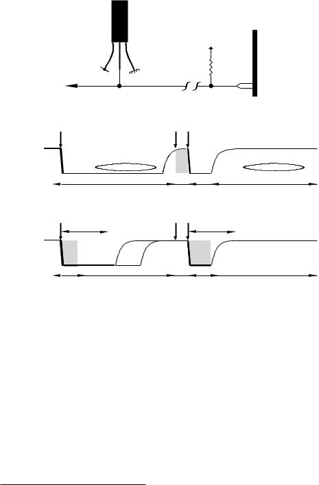
This subroutine releases both the SCL and SDA lines which are then pulled high to ensure the bus is in its Idle state for the minimum duration 1.3 µs tBUF. Bringing SDA low gives the characteristic Start \ , which is fol-
lowed by a 0.6 µs delay to implement tHD;STA (see Fig. 12.17) before the subroutine exits with both SCL and SDA low.

332 The Quintessential PIC Microcontroller
Program 12.7 Low-level I2C subroutines.
; *************************************************************
; * |
FUNCTION: |
Outputs the Start |
condition |
|
|
* |
||
; |
* |
ENTRY |
: |
FSR points to the |
I2C port’s |
TRIS |
register |
* |
; |
* |
EXIT |
: |
Start condition and SCL, SDA |
pins |
low |
* |
|
; *************************************************************
START |
bsf |
INDF,SDA |
; Ensure that we start with the |
|
bsf |
INDF,SCL |
; Data and Clock lines pulled hi |
|
Delay_600 |
; 1.3us delay in Idle state |
|
|
Delay_600 |
|
|
|
bcf |
INDF,SDA |
; Low-going edge on Data line |
|
Delay_600 |
; Wait for Slave to detect this |
|
|
bcf |
INDF,SCL |
; Exit with the Clock line low |
|
return |
|
|
; *************************************************************
; * |
FUNCTION: |
Outputs the Stop condition |
* |
||
; |
* |
ENTRY |
: |
FSR points to the I2C port’s TRIS register |
* |
; |
* |
EXIT |
: |
Stop condition and SCL, SDA pins high (Idle) |
* |
; *************************************************************
STOP |
bcf |
INDF,SCL |
; Make sure that Clock line is low |
|
bcf |
INDF,SDA |
; and the Data line is low |
|
bsf |
INDF,SCL |
; Bring Clock line high |
|
Delay_600 |
; for a minimum of 0.6us |
|
|
bsf |
INDF,SDA |
; Rising edge on Data signals Stop |
|
return |
|
; including the return time |
;*************************************************************
;* FUNCTION: Transmits byte to Slave and monitors Acknowledge*
; * |
ENTRY |
: |
8-bit data |
to be TXed is in DATA_OUT |
* |
|||
; * |
RESOURCE: |
START and STOP subroutines |
* |
|||||
; |
* |
EXIT |
: |
Byte |
transmitted. ERROR |
is 01 IF no Ack received* |
||
; |
* |
EXIT |
: |
from |
Slave |
ELSE 00. SCL |
low |
* |
; *************************************************************
I2C_OUT bcf |
INDF,SCL |
; Make sure that Clock line is low |
clrf |
ERR |
; Start with no error |
movlw |
8 |
; Loop counter = 8 |
movwf |
COUNT |
|
I2C_OUT_LOOP |
|
|
bcf |
INDF,SDA |
; Data bit low? |
rlf |
DATA_OUT,f |
; Shift data left once into Carry |
btfsc |
STATUS,C |
; Is C 0 or 1 |
bsf |
INDF,SDA |
; IF the latter THEN make Data hi |
Delay_600 |
; Delay plus xtra instructions OK |
|
Delay_600 |
|
|
bsf |
INDF,SCL |
; Bring Clock pin high |
Delay_600 |
; for at least 0.6us |
|
bcf |
INDF,SCL |
; Bring Clock low |
decfsz |
COUNT,f |
; Decrement loop count |
goto |
I2C_OUT_LOOP |
; and repeat eight times |
; Now check Acknowledge from Slave |
||
bsf |
INDF,SDA |
; Release Data line |
Delay_600 |
; Keep Clock line low |
|
Delay_600 |
; long enough for Slave to respond |
|
bsf |
INDF,SCL |
; Bring Clock line high |
btfsc |
INDF,SDA |
; Check if Data is low from Slave |
incf |
ERR,f |
; IF not THEN ERROR1 |
bcf |
INDF,SCL |
; Now finish ACK by bringing Ck lo |
return |
|
|
|
|
|

12. One Bit at a Time 333
STOP
The Stop condition is implemented by ensuring that both SCL and SDA lines are low (which should be the case after an Acknowledge condition) and then releasing the SCL line which is then pulled high. After a 0.6 µs
delay to implement tSU;STO SDA is released to give the characteristic Stop / . The subroutine exits with both lines released and the bus Idling
in preparation for the next Start condition.
I2C_OUT
This subroutine clocks out the eight bits placed in DATA_OUT by the caller, MSB first, and then checks that the Slave has Acknowledged the transaction.
The first part of this process is implemented by repetitively shifting the datum in DATA_OUT and inspecting the Carry flag. SDA is set to mirror
C and the SCL line toggled to accord with the tLOW and tHIGH parameters illustrated in Fig. 12.17.
Once the loop count reaches zero, the Data line is released with SCL
low for the duration tLOW. SCL is then released high and the state of SDA, which should have been dragged low by the Slave, checked. If not low, the
No ACKnowledge (NACK) situation is returned with ERR = 01h; otherwise it will be zero.
Our use of errors here is very rudimentary. For instance, errors can also occur if some other device has locked either line low; that is the bus is busy.
We have not coded a Master-Receive I2C counterpart to subroutine I2C_OUT, as the MAX518 only demands a Master-Transmit data interchange. However, Program 12.14 gives the I2C_IN mirror.
As our example we will send the contents of File 20h to the MAX518 Channel 0 and then the contents of File 21h to Channel 1; at that point updating both DAC registers and hence simultaneously outputting the
analog equivalent of File 20h to pin Vout0 and File 21h to pin Vout1. We assume that both AD0 and AD1 pins are connected to Ground.
Our implementation will involve the transmission of a packet of five bytes of information sandwiched between a Stop and a Start condition.
1.Start condition.
2.Address byte: 01011000b
Slave address 01011(00), Write.
3.Command byte 1: 00000XX0b
No ReSeT, no Power Down, Channel 0.
4.Data byte 1: Contents of File 20h.
5.Command byte 2: 00000XX1b
No ReSeT, no Power Down, Channel 1.
6.Data byte 2: Contents of File 21h.
7.Stop condition.


12. One Bit at a Time 335
enabled and programmed in Mode 11 (Slave idle – see Table 12.1) these pins conform to the specified relatively slow (300 ns maximum) rise and fall times. A normal port line has transition times of the order of 10 ns. The slower transition times give less cross talk between bus lines and less transmission line reflections at electrical discontinuities.
As in the case for the SPI protocol, many C compilers targeted to the PIC have built-in functions to implement the I2C protocol and avoid bit banging user-defined functions.
To illustrate the technique, consider Program 12.9 which replicates the assembly-level coding of Programs 12.7 and 12.8 using the CCS compiler.
i2c_start();
Generates the Master Start condition.
i2c_stop();
Generates the Master Stop condition.
i2c_read();
Reads a byte over the bus. If an optional parameter of 0 is used then the Master will not Acknowledge the received data.
Program 12.9 Interfacing to the MAX518 in C.
#include <16F84.h> |
|
|
|
|
/* PortA, bit0 is the Master SCL, bit1 is the Master SDA, |
|
|||
|
fast protocol |
|
|
*/ |
#use i2c(master, scl=PIN_A0, sda=PIN_A1, fast) |
|
|||
#define data_x *(unsigned int *)0x20 |
|
|||
#define data_y *(unsigned int *)0x21 |
|
|||
void MAX518(unsigned int channel_0, unsigned int channel_1); |
|
|||
main() |
|
|
|
|
{ |
|
|
|
|
/* |
Various code lines |
|
*/ |
|
MAX518(data_x, data_y); /* |
Send out the two data bytes |
*/ |
||
/* |
More code |
|
|
*/ |
} |
|
|
|
|
void MAX518(unsigned int channel_0, unsigned int channel_1) |
|
|||
{ |
|
|
|
|
i2c_start(); |
/* |
Start condition |
*/ |
|
i2c_write(0x58); |
/* |
Send out Slave address; Write |
*/ |
|
i2c_write(0); |
/* |
Send out Command 1 |
*/ |
|
i2c_write(channel_0); /* |
Send out datum to channel 0 |
*/ |
||
i2c_write(0x01); |
/* |
Send out Command 2 |
*/ |
|
i2c_write(channel_1); /* |
Send out datum to Channel 1 |
*/ |
||
/* Updates both channels |
|
|
*/ |
|
i2c_stop(); |
/* |
Stop condition |
*/ |
|
} |
|
|
|
|
|
|
|
|
|

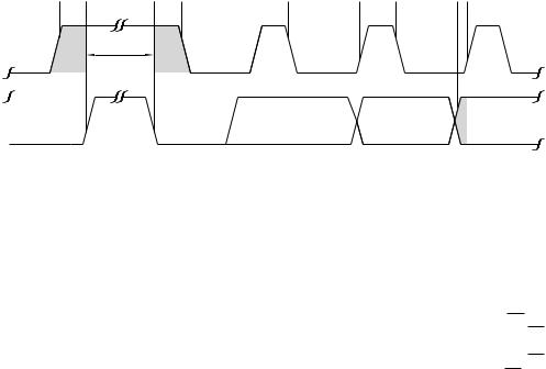
12. One Bit at a Time 337
two Stop bits. This requires a transmission rate of 110 bits per second, or 110 baud.10
The first purely electronic terminals required only one Stop bit, and could print at 30 characters per second, giving a rate of 300 baud. Traditionally communication channels use multiples of 300; eg. 1200, 2400, 4800, 9600…. PC serial ports can run up to 19,200 baud. However, this ×300 rate is not necessary as long as receiver and transmitter are running at the same nominal rate.
Typically a receiver on detecting an incoming datum will try and sample each bit at approximately mid point. This means that a frequency drift of ±0.5 bit time can be tolerated in the space of ten bits. Thus the receiver and transmitter local clocks must be within ±5%. The two will be resynchronized at the start of each datum.
Although not the most e cient of techniques, the asynchronous protocol outlined here has the major advantage of being an international standard. There are several variants; for instance the word can typically be from five to nine bits long. In our example the word length is eight bits with the eighth bit being used to provide a limited error checking capability. This parity bit is set in our example so that the number of 1s in the word is always odd. This can be checked at the receiver (see SAQ 3.9 on page 73) to detect a single bit error.
The original teleprinter code developed by Emile Baudot in 1875 is only five bits long.11 Here the string "PIC" is coded as 10110 00110 01110. Although limited in capability, its key advantage over Morse code (Samual Morse, 1840) was its fixed length (compare with ·– – ···– ·–·) which considerably simplifies the design of the transmitter and receiver. However, Morse code is more e cient as the number of bits is approximately inversely proportionally to a letter’s statistical frequency of use.
The 7-bit ASCII code of Table 1.1 on page 5, first adopted in 1963, was the first code specifically developed for computer communication systems. In 8-bit systems the extra 128 code patterns is usually utilized to add a selection of accented, mathematical and graphic symbols rather than for parity. However, parity can be accommodated by using a 9-bit word format.
For our example we have adopted a format of one Start, eight data with no parity and one Stop bit. Using a bit banging approach, as we have already done for our SPI and I2C protocols, is straightforward provided
10Strictly the baud rate is a measure of information rate. For a simple baseband system this is equal to the bit rate. However, this equality is not always true. For example, a
telephone modem can use a di-bit modulation scheme where groups of bits two at a time give a carrier tone phase shift of 0◦, 90◦, 180◦ and 270◦ phase shift for the patterns 00, 01, 10, 11 respectively. In this case the baud rate is four times the bit rate.
11Actually the first binary coded alphanumeric code was devised by Francis Bacon in around 1600. It too was a 5-bit code.

338 The Quintessential PIC Microcontroller
that we have an accurate 12 -bit delay. For example, for a 4800 baud link this would be 104 µs. As the delay is so short we can use an in-line approach using a macro in the same manner as in Program 12.6 rather than the subroutine approach of Program 6.8 on page 159.
Program 12.10 A baud-rate delay macro showing a half 9600 baud period delay at 20 MHz evocation.
include "p16F84a.inc" #define XTAL d’20’ #define BAUD d’9600’
#define N (XTAL*d’980000’)/(8*BAUD)
Baud_delay macro |
|
|
|
|
local |
BAUD_LOOP |
|
|
if(XTAL>d’12’) |
|
|
|
movlw |
N/9 |
; The delay parameter |
BAUD_LOOP |
addlw |
-1 |
; Decrement |
|
nop |
|
|
|
nop |
|
|
|
nop |
|
|
|
nop |
|
|
|
nop |
|
|
|
btfss |
STATUS,Z ; Until zero |
|
|
goto |
BAUD_LOOP |
|
|
endif |
|
|
|
if((XTAL>=6)&&(XTAL<=d’12’)) |
||
|
movlw |
N/5 |
; The delay parameter |
BAUD_LOOP |
addlw |
-1 |
; Decrement |
|
nop |
|
|
|
btfss |
STATUS,Z ; Until zero |
|
|
goto |
BAUD_LOOP |
|
|
endif |
|
|
|
if(XTAL<6) |
|
|
|
movlw |
N/4 |
; The delay parameter |
BAUD_LOOP |
addlw |
-1 |
; Decrement |
|
btfss |
STATUS,Z ; Until zero |
|
|
goto |
BAUD_LOOP |
|
|
endif |
|
|
|
endm |
|
|
|
|
|
|
The macro shown in Program 12.10 is designed to give a suitable 12 - bit delay for a range of baud rates from 1200 through 9600 and crystal frequencies of 4 through 20 MHz. Both BAUD and XTAL constants are defined in the program head by the programmer; the example given in the listing showing a baud rate of 9600 and crystal frequency of 20 MHz.
The kernel of our macro is the decrement loop:

|
|
|
|
12. One Bit at a Time 339 |
|
|
|
|
|
movlw |
K |
; |
1˜ |
; K is the delay const |
BAUD_LOOP addlw |
-1 |
; |
K˜ |
; Decrement |
btfss |
STATUS,Z ; |
((K-1)+2)˜ ; until zero |
||
goto |
BAUD_LOOP; |
2(K-1)˜ |
|
|
|
|
|
|
|
which gives a total of 4K cycles delay, where each cycle is 4/XTAL microseconds. This can be increased by padding with nop instructions, each adding K cycles to the total.
For any given baud rate we require |
106 |
|
microseconds for a |
1 |
bit |
|||||||||||
2×BAUD |
2 |
|||||||||||||||
|
|
|
|
|
|
|
|
|
|
|
|
|
||||
period delay; so to evaluate the value of K we need to calculate the total |
||||||||||||||||
number N of 4/XTAL cycles. |
|
|
|
|
|
|||||||||||
|
4 |
|
|
|
|
|
106 |
|
|
|
|
|
|
|||
N × XTAL = |
2 |
× |
BAUD |
|
|
|
|
|
||||||||
|
|
|
|
|
|
|
||||||||||
|
N |
= |
|
106 × XTAL |
|
|
|
|
|
|||||||
|
|
|
8 |
× |
BAUD |
|
|
|
|
|
||||||
|
|
|
|
|
|
|
|
|
|
|||||||
In the macro of Program 12.10 N has been defined accordingly. To determine the constant to be loaded into W at the beginning of the loop this value is divided by the total delay cycles in the loop. For example, if XTAL is greater than 12 MHz then the five extra nop instructions bring the total delay to nine cycles, hence the initial constant K is N/9. Actually the value of K is can be reduced by around 2% to compensate for the instructions outside the macro; hence the use of 980,000 in Program 12.10 in the definition of N rather than 1,000,000 (106).
Notice the use of the local directive to qualify a label inside a macro; in this case BAUD_LOOP. This ensures that when the macro is used several times, the assembler will not object to the same named label appearing more than once in the one program.
With our delay macro in situ, the basic input/output subroutines of Program 12.11 are similar to our bit banging SPI subroutines. The PUTCHAR subroutine simply brings the TX pin low for two Baud_delay periods and then toggles the pin eight times mirroring the data in DATA_OUT least-significant bit first – the opposite order to SPI/I2C. Finally TX is held high for the same period to give the Stop/Idle condition.
The input GETCHAR counterpart is more complex. After an Idle state a low-going voltage at pin RX will be treated as a Start bit. However, if the data stream is subsequentially sampled at intervals of one bit period (two evocations of Baud_delay) then as this is just at the transition point of the transmitter, any drift in the two clock rates may cause errors. To avoid this, a half bit period is evoked and then the state of RX checked to ensure that the Start bit is still present. If it is, then subsequent samples are taken at two Baud_delay periods, which is approximately at the bit center point. Better noise rejection could be obtained by sampling at a

340 The Quintessential PIC Microcontroller
Program 12.11 Asynchronous formatted input and output subroutines.
;*************************************************************
;* FUNCTION: Transmits one 8-bit byte in asynchronous format *
;* FUNCTION: Baud rate can be 1200 - 9600 for XTAL 1 -- 20MHz*
; * |
RESOURCE: |
Macro |
Baud_delay giving a |
0.5 |
bit delay; COUNT |
* |
|||
; |
* |
ENTRY |
: |
8-bit |
datum |
in DATA_OUT, XTAL |
& BAUD predefined * |
||
; |
* |
EXIT |
: |
Contents of |
DATA_OUT 00h, |
byte TXed |
* |
||
; *************************************************************
PUTCHAR |
movlw |
8 |
; Eight data bits |
|
movwf |
COUNT |
|
|
bcf |
PORTA,TX |
; Start bit |
|
Baud_delay |
; 2x0.5 bit delay |
|
|
Baud_delay |
|
|
; Now shift out data, LSB first |
|
||
PUTCHAR_LOOP rrf |
DATA_OUT,f |
; Rotate right into Carry |
|
|
btfss |
STATUS,C |
; Test Carry bit |
|
goto |
ITS_A_0 |
; IF 0 THEN output a 0 |
|
bsf |
PORTA,TX |
; ELSE output a 1 |
|
goto |
PUTCHAR_NEXT |
; and continue |
ITS_A_0 |
bcf |
PORTA,TX |
; Output a 0 |
PUTCHAR_NEXT |
Baud_delay |
; One-bit duration |
|
|
|||
|
Baud_delay |
|
|
|
decfsz |
COUNT,f |
; Repeat eight times |
|
goto |
PUTCHAR_LOOP |
|
|
bsf |
PORTA,TX |
; Stop bit |
Baud_delay
Baud_delay return
; *************************************************************
; * FUNCTION: |
Receives one 8-bit byte in asynchronous format |
* |
|
; * FUNCTION: |
Baud rate can be 1200 - 9600 for XTAL 1 -- 20MHz* |
||
; * RESOURCE: |
Macro BAUD_DELAY giving a 0.5 bit delay; COUNT |
* |
|
; * ENTRY |
: |
XTAL & BAUD predefined |
* |
; * EXIT |
: |
DATA_IN holds the received byte. |
* |
; * EXIT |
: |
Err is 00 if no Framing error ELSE -1 |
* |
; *************************************************************
GETCHAR |
movlw |
8 |
; Eight data bits |
|
movwf |
COUNT |
|
|
clrf |
ERR |
; Zero Error byte |
GETCHAR_START |
btfsc |
PORTA,RX |
; Poll for 0 |
|
|||
|
goto |
GETCHAR_START |
|
|
Baud_delay |
; Hang around for 0.5 bit time |
|
|
btfsc |
PORTA,RX |
; Check; is it still low? |
|
goto |
GETCHAR_START |
|
|
Baud_delay |
; IF yes THEN hang around |
|
|
Baud_delay |
|
|
GETCHAR_LOOP bcf |
STATUS,C |
; Clear Carry |
|
|
rrf |
DATA_IN,f |
; Shift 0 into datum |
|
btfsc |
PORTA,RX |
; Check; is input high? |
|
bsf |
DATA_IN,7 |
; IF yes THEN set bit in datum |
|
Baud_delay |
|
|
|
Baud_delay |
|
|
|
decfsz |
COUNT,f |
; Do eight times |
|
goto |
GETCHAR_LOOP |
|
|
btfss |
PORTA,RX |
; Look for a Stop bit (High) |
|
decf |
ERR,f |
; IF low THEN signal an error |
|
return |
|
|
|
|
|
|

 f/4
f/4

12. One Bit at a Time 345
Program 12.12 The USART-based I/O subroutines.
;*************************************************************
;* FUNCTION: Transmits one 8-bit byte in asynchronous format *
; * |
RESOURCE: |
PIC USART |
* |
||
; |
* |
ENTRY |
: |
8-bit datum in DATA_OUT |
* |
; |
* |
EXIT |
: |
Contents of DATA_OUT unchanged, byte TXed |
* |
; *************************************************************
PUTCHAR btfss |
PIR1,TXIF |
; Check, |
is TX buffer full? |
||
goto |
PUTCHAR |
; IF not |
THEN try again |
||
movf |
DATA_OUT,w |
; |
ELSE get |
datum |
|
movwf |
TXREG |
; |
and copy |
to USART TX register |
|
return |
|
|
|
|
|
; *************************************************************
; * FUNCTION: |
Receives one 8-bit byte in asynchronous format |
* |
|
; * RESOURCE: |
PIC USART |
* |
|
; * ENTRY |
: |
None |
* |
; * EXIT |
: |
DATA_IN holds the received byte. |
* |
; * EXIT |
: |
ERR is 00 if no error. Framing ERRor only = -1 |
* |
; * EXIT |
: |
ERR = -2 if Overflow ERRor and -3 if both types * |
|
; *************************************************************
GETCHAR clrf |
ERR |
; Zero flag byte |
btfss |
PIR1,RCIF |
; Check, is there a char ready? |
goto |
GETCHAR |
; IF not THEN try again |
; Error return |
|
|
btfss |
RCSTA,FERR |
; Was there a Framing error? |
goto |
CHECK_OERR |
; IF not THEN check for Overflow |
movlw |
-1 |
; ELSE record a Framing error |
CHECK_OERR |
|
|
btfsc |
RCSTA,OERR |
; Check for Overflow ERRor |
goto |
GET_EXIT |
; IF none THEN complete |
decf |
ERR,f |
; Otherwise register error |
decf |
ERR,f |
|
bcf |
RCSTA,CREN |
; and reset the logic |
bsf |
RCSTA,CREN |
|
GET_EXIT |
|
|
movf |
RCREG,w |
; Get datum |
movwf |
DATA_IN |
; and put away |
return |
|
|
|
|
|
Some systems may not wish the processor to hang up waiting for a character which is a long time in coming. In such cases an alternative input subroutine, perhaps called getch, could return an ERR of −1 if the return was empty handed. Another approach would be to generate an interrupt each time an incoming character is sensed rather than using a polling technique.
In the case of the CCS C compiler the #use rs232 directive tells the compiler which pins are to be used for RX and TX. The normal C I/O functions, such as printf(), use these pins as their link to the standard

346 The Quintessential PIC Microcontroller
channel. If these pins are specified as PIN_C6 and PIN_C7 then where the part has a built-in USART this will be used instead of a software technique.
There is more to setting up a communication link than establishing a suitable protocol. PIC devices have normal logic voltage and current levels which are not intended for connections greater than 30 cm (1 ). Although with care14 distances considerably in excess of this can be employed, in situations with relatively fast bit rates di erent signalling techniques have to be used.
In the era of electromechanical TTYs the de facto 20 mA loop standard was in common use. This uses zero and 20 mA current to signal logic 0 and logic 1 respectively. Use of current means that line attenuation is not a problem (as current out must equal current in) and this level of current was su cient to directly activate the receiver solenoid relay.
Current sources are realized by using high voltages in series with a large resistance. The latter gives long time constants, which, while adequate in the area of 110 baud rates, did not transfer well to the introduction of electronic terminals, UARTs and modems. RS-23215 was introduced in 1969 as the standard interface for connecting an item of Data Terminal Equipment (DTE), such as a terminal, to approved Data Circuit terminating Equipment (DCE), typically a modem. Thus, not only did it define signalling levels, as shown in Fig. 12.20(a), but also various control and handshake lines, some of which are shown in Figs. 12.20(d) and 12.21. For example the modem would signal back to the DTE that a telephone link had been opened with the remote DTE by activating the Clear To Send (CTS) handshake signal. Two data lines plus a ground line are needed for a full duplex transmission circuit.
The RS-232 standard has a range of 15 m (50 ) at a maximum rate of 20 kbaud, which it achieves by mapping logic 0 (often called a space) to typically +12 V and logic 1 (often called a mark) to typically −12 V. The receiver can distinguish levels down to ±5 V. The RS-423 standard (1978) in Fig. 12.20(b) is similar but can manage 1.2 km (6000 ) at up to 80 kbaud and 10 Mbaud at 12 m (40 ) with up to ten receivers.
Both RS-232 and RS-423 are unbalanced (or single-ended) standards, where the receiver measures the potential between signal line and ground reference. Even though the transmitter and receiver grounds are usually connected through the transmission line return, the impedance over a long distance may support a significant di erence in the two ground potentials, which will degrade noise immunity. Furthermore, any noise induced from outside will a ect signal lines di erently from the ground return due to their dissimilar electrical characteristics – hence the name unbalanced.
14Or sometimes ignorance!
15Defined in USA as the Electronics Industries Association EIA 232-E standard and as the V24 interface by the CCITT in Europe.
|
|
|
|
|
|
|
|
RS-422A: 1 |
driver |
and up to 10 |
receivers |
|
|
|
Logic levels |
|
1 driver and 1 receiver |
|
Enable |
RS-485: 32 driver/receiver pairs |
|
|
|
||||
|
|
|
|
|
Logic levels |
Logic levels |
|
|
|
|
Logic levels |
|
|
|
|
|
|
|
|
B |
|
|
B |
|
|||
|
|
|
±12 V |
|
±3 V |
|
|
|
|
|
|
||
|
D |
|
|
R |
D |
±5 V |
|
|
±200 mV |
R |
|
||
|
|
|
|
|
|
|
|
A |
|
|
A |
|
|
.Fig |
|
|
15m @ 20kb |
|
|
|
|
|
15m @ 10Mb |
|
|
|
|
12 |
|
|
|
|
Enable |
|
|
|
|
|
|||
|
|
|
|
|
|
|
150m @ 1Mb |
|
|
|
|||
|
|
|
|
|
|
|
|
|
|
|
|||
. |
|
|
|
|
|
|
Logic levels |
|
|
1km @ 100kb |
|
Logic levels |
|
20 |
|
|
|
|
|
|
B |
|
|
|
|||
|
|
|
|
|
|
|
|
|
|
|
|
||
|
|
|
|
|
|
|
|
|
|
|
|
|
|
Some |
|
|
|
|
|
|
D |
|
|
|
|
R |
|
|
|
|
|
|
|
|
A |
|
|
|
|
|
|
|
|
|
|
|
|
RS485 only |
|
|
|
|
|
||
signalling |
(a) RS-232C |
|
|
|
(b) RS-422/485 |
|
|
|
|
|
|||
|
1 |
driver and up to 10 |
receivers |
|
|
|
|
|
|
|
|
||
Logic levels |
|
|
|
|
Logic levels |
|
|
|
|
|
|
|
|
.configurations |
D |
|
±12V |
|
±200 mV |
R |
UART Logic levels |
|
|
|
|
Logic levels UART |
|
|
|
|
|
|
|
1070 Hz |
|
|
|||||
|
|
|
|
|
|
|
|
|
|
|
|
||
|
|
|
|
|
|
TX_DATA |
Modem |
|
1270 Hz |
Modem |
TX_DATA |
One .12 |
|
|
|
|
|
|
|
|
2025 Hz |
||||||
|
|
|
|
|
|
RX_DATA |
|
2225 Hz |
RX_DATA |
||||
|
|
10m |
@ 100kb |
|
DCD |
|
|
DCD |
|||||
|
|
|
CTS |
|
|
CTS |
|||||||
|
|
100m @ 10kb |
|
|
|
|
|||||||
|
|
|
Logic levels |
RTS |
|
|
RTS |
||||||
|
|
1km |
@ 1kb |
|
|
|
|||||||
|
|
|
|
|
|
|
|
|
|
|
Bit |
||
|
|
|
|
|
|
R |
|
|
|
|
|
|
|
|
|
|
|
|
|
|
|
|
|
|
|
Time a at |
|
|
(b) RS-423A |
|
|
|
(d) FSK |
|
|
|
|
|
|||
|
|
|
|
|
|
|
|
|
|
||||
|
|
|
|
|
|
|
|
|
|
|
|
|
347 |
348 The Quintessential PIC Microcontroller
The RS-422 (1978) and RS-485 (1983) standards are described as balanced. Here each signal link comprises two conductors, normally twisted around each other, known as twisted pair. The logic level is represented as the di erence of potential across the conductors, not the di erence from ground. Calling the conductors A and B, then logic 0 is represented as A<B and logic 1 by A>B. A di erence of more than ±200 mV at the receiver is su cient to establish the logic level and the transmitter will typically generate a ∆V = ±5 V. As the A and B conductors have the same characteristics and are tightly wound together they represent similar targets for induced noise. As the same noise voltage appears in both conductors and the receiver only distinguishes di erences, rejecting commonmode voltages up to ±7 V, then the noise immunity of these balanced links is clearly superior to unbalanced schemes. Commercial twistedpair cables, used in Local Area Networks (LANs), often carry three or four pairs of conductors, each link having a di erent twist pitch to reduce induction between links.
The main di erence between the RS-422 and RS-485 standards is the provision in the latter case for multiple transmitters as well as receivers to implement multi-drop LANs. As only one transmitter can be active at any one time, an RS-485 transmitter bu er must have an enable input, to select the master device. The single RS-422 transmitter has no need to be disabled.
RS-232 was originally designed for DTE-modem interconnection, although its use is now much more varied – see Fig. 12.21. Figure 12.20(d) shows a simple Frequency Shift Keying (FSK) full duplex system with the mark/space of one channel being represented by the tones 1070/1270 Hz and the other by 2025/2225 Hz; frequencies which fit well inside the normal telephone link bandwidth of 300 – 3400 Hz. Handshake lines DCD (Data Carrier Detect), CTS (Clear TO Send) and RTS (Ready To Send) are used to control the sequence of operations prior to and terminating the communication of data.
Many modem schemes currently use Phase Shift Keying (PSK) where typically at least eight di erent phases in 45◦ steps of a single tone are used to encode 3-binary bit code groups (tri-bits) in any one time slot. In this way the baud rate may be increased with the same signalling rate, albeit at the expense of noise immunity, as witnessed by the steady increase in PC-based home telephone internet data rates in recent years up to 56 kbaud.
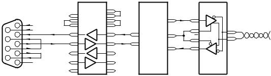
As an example, Fig. 12.21 shows the connection between a PIC and the serial port of a PC – or any device with an asynchronous RS-232 port. The Maxim MAX233 dual RS-232 transceiver translates from +12 V to 0 V (logic 0) and −12 V to +5 V (logic 1). If handshake lines are not being used, as is usual in simple links, the PC can be ‘fooled’ into treating the interface as ready to accept data by linking as shown in the diagram. For


12. One Bit at a Time 351
Program 12.14 Reading in a byte using the I2C protocol.
;*************************************************************
;* FUNCTION: Reads in byte from Slave with optional ACK/NACK *
; * |
ENTRY |
: |
ACKNO |
= 00 for |
ACK ELSE NACK |
* |
|
; * |
RESOURCE: |
START |
and STOP |
subroutines, Delay_600 macro |
* |
||
; |
* |
EXIT |
: |
DATA_IN holds datum sent from slave |
* |
||
; |
* |
EXIT |
: |
ACK or NACK sent to Slave, SCL low |
* |
||
; *************************************************************
I2C_IN |
bcf |
INDF,SCL |
; Make sure that Clock line is low |
|
movlw |
8 |
; Loop count = 8 |
|
movwf |
COUNT |
|
I2C_IN_LOOP |
|
|
|
|
bcf |
INDF,SCL |
; Clock low |
|
Delay_600 |
; For minimum period |
|
|
Delay_600 |
|
|
|
bsf |
INDF,SCL |
; Clock high |
|
bcf |
STATUS,C |
; Carry = 0 |
|
btfsc |
INDF,SDA |
; Check state of incoming bit? |
|
bsf |
STATUS,C |
; IF 1 THEN make Carry = 1 |
|
rlf |
DATA_IN,f |
; and rotate it into the datum |
|
decfsz |
COUNT,f |
; Decrement loop count |
|
goto |
I2C_IN_LOOP |
; and repeat eight times |
; Now determine if Acknowledge is to be sent |
|||
|
bcf |
INDF,SCL |
; Clock low |
|
bsf |
INDF,SDA |
; Data output float (NACK) |
|
movf |
ACKNO,f |
; Test the caller’s wish |
|
btfsc |
STATUS,Z |
; IF non zero THEN leave as NACK |
|
bcf |
INDF,SDA |
; ELSE bring low to signal ACK |
|
Delay_600 |
; Keep Clock low |
|
|
Delay_600 |
|
|
|
bsf |
INDF,SCL |
; Now high |
|
Delay_600 |
|
|
|
bcf |
INDF,SCL |
; Leave with Clock low |
|
return |
|
|
to the I2C time and protocol specification as in our I2C_OUT subroutine of Program 12.7. In this protocol the Master signals back to the Slave to stop sending data by letting the SDA line float high in the Acknowledge slot in the ninth clock pulse – see Fig. 12.13. The normal low state in this slot is called ACK, whilst the deviant high Acknowledge state is called NACK (No ACKnowledge). To cope with both these situations our I2C_IN optionally generates either situation depending on the state of the variable ACKNO set by the caller. If file register ACKNO is zero on entry then a normal low ACK is sent in this slot. Any non-zero value in this variable causes a high NACK to be sent back to the Slave. The Slave then terminates its transmission and listens for the next Stop/Start condition.

12. One Bit at a Time 353
cating with the Master PIC. This is encapsulated in the messages shown in Fig. 12.23.
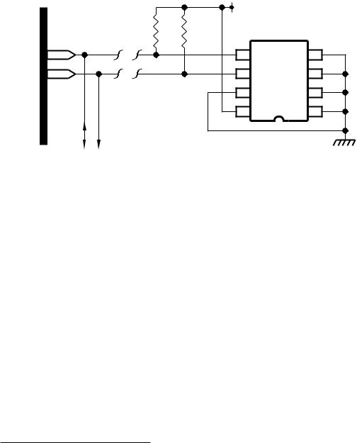
In all cases the Master initiates a data transfer by sending a Start condition followed by a Command byte. The Control byte contains the I2C Slave address 1010; the chip select address A2 A1 A0 and the R/W bit in
the order 1 
 0
0  1
1 
 0
0  A2
A2 
 A1
A1  A0
A0  R/W . Although the chip select address is shown as part of the Command byte and the three corresponding pins are shown in Fig. 12.22, newer versions of the smaller EEPROMS do not implement this feature. This is because if EEPROM capacity needs to be expanded then it more e cient to replace the device by a pin-identical larger version. For example replacing a 24LC01B by a 24LC08B gives an eightfold increase with no hardware alteration. Larger EEPROMS, such as the 24LC256 do implement chip select address as the method of expansion as additional devices will need to be hung on the bus in this situation. Eight 24LC256s will give a capacity of 256 kbyte of non volatile memory.
This is normally followed by the address in the EEPROM that data is to be written into or read out of. In the specific case of the 24LC01B the data is arranged as 128 cells, each comprising a byte that can be individually written to or read from. This means that a 7-bit address will fit comfortably in the 8-bit address byte. This scheme will cope with devices up to the 24LC02B but beyond this addresses greater than 8 bit wide are needed. This is done by using the Chip select bits in the Command bit, giving an address width of 11 bits and a capacity of 2 kbytes (16 kbits). For EEPROMs larger than the 24LC16 two Address bytes are used following the Command byte.
The process of sending the byte address to the EEPROM is implemented as a Write action in Fig. 12.23. This is actioned by setting the R/W bit low in the command bit. Where a data byte is to be written into the addressed location this byte comes immediately after the Address byte and then followed by a Stop condition. If more than one data byte is transmitted before the Stop then this data is stored in a small on-board bu er and the actual programming will not occur until the Stop condition. The 24LC01B can store eight bytes at a time in a single page, with the lower three address bits being incremented on each data byte sent. If this address rolls over, earlier addressed data will be overwritten. The size of this page depends on the device; for example, the 24LC256 uses a 64-byte page. In Fig. 12.23(a) three bytes are shown being written into the 24LC01B. As these locations are to be targeted in the bottom three locations, 00-01-02h, then roll-over will not occur.
As soon as the Stop condition is received the 24LC01B will commence programming the targeted cells with the bu ered data. This process takes typically 2–5 ms across the family. If the Master attempts to initiate a process during this time then the EEPROM will not Acknowledge

12. One Bit at a Time 357
The various DS1820 functions, such as Convert (44h), Read temperature (BEh), are initiated by the Master sending the appropriate data as 8-bit codes, each byte comprising a Start condition ( \ ) and eight Write
slots, as shown in Fig. 12.24(b). As in the I2C case, the data line DQ is pulled high with a pull-up resistor and the Master simulates the logic 1 state by changing its port line from low to input (see Fig. 12.14(b)). In this state the Master can listen to data sent by the Slave as shown in Fig. 12.24(c).
For our example we are required to write two subroutines that will respectively write a byte to a 1-Wire Slave and read a byte from the Slave.
Solution
From Fig. 12.24(b) we see that writing a bit to a Slave involves the following tasks:
1.The Master starts the process by forcing the data line low for at least 1 µs.
2.The Master either keeps the line low (Write 0) or releases the line (Write 1) for 60 – 120 µs.
3.The Slave reads the line state between 15 – 45 µs later.
4.The Master releases the line (if Write 0) for at least 1 µs to relax the system.
The subroutines of Program 12.16 assume that the port line driving DQ has been set up as described on page 325 for the I2C bus to give the two states as hard low and open circuit – pulled up high. Also we assume that we have the delay macro Delay_us in situ which gives a Kµs delay, where K is the parameter passed to the macro.
Delay_us macro |
K |
; K is the |
number of usec delay |
local |
DELAY_US_LOOP |
|
|
movlw |
(K*XTAL)/(4*3)+1 ; |
1˜ |
|
DELAY_US_LOOP |
|
|
|
addlw |
-1 |
; Decrement count: N˜ |
|
btfss |
STATUS,Z ; to zero |
: N + 1˜ |
|
goto |
DELAY_US_LOOP ; |
: 2(N-1)˜ |
|
endm |
|
|
|
|
|
|
|
Both subroutines begin by driving DQ low for a minimum of 1 µS, defining the Start condition. Writing a single bit to DQ occurs in a slot which has a duration of 60 – 120 µs, and commences with DQ either low or released to be pulled high, defining a Write-0 or Write-1 condition. The Slave samples the state of the data line sometime after 15 µs into the slot. Although the duration of the slot is not critical, care needs to be taken as a low duration of between 480 and 960 µs is interpreted by the Slave as a Reset command (see SAQ 12.3).

358 The Quintessential PIC Microcontroller
Program 12.16 Reading and writing on a 1-Wire system.
; *************************************************************
; * |
FUNCTION: |
Writes a |
byte datum to a 1-Wire slave |
* |
||||
; * |
RESOURCE: |
macro |
Delay_us giving N microsecond delay |
* |
||||
; |
* |
ENTRY |
: |
Datum |
is |
in |
DATA_OUT |
* |
; |
* |
EXIT |
: |
DATA_OUT |
is |
zero, W, STATUS altered |
* |
|
; *************************************************************
WRITE_1W movlw |
8 |
; Loop count |
movwf |
COUNT |
|
W_LOOP bcf |
INDF,DAT |
; Low edge signals Start |
Delay_us |
1 |
; for 1us |
rrf |
DATA_OUT,f |
; LSB first shift into Carry |
btfsc |
STATUS,C |
; Was it a 1? |
bsf |
INDF,DAT |
; IF it was THEN output high |
Delay_us |
d’60’ |
; Hold for 60us |
bsf |
INDF,DAT |
; Release line to go high |
Delay_us |
1 |
; Relax for 1us |
decfsz |
COUNT,f |
; Repeat eight times |
goto |
W_LOOP |
|
return |
|
|
; *************************************************************
; * |
FUNCTION: |
Reads a byte datum from a 1-Wire slave |
* |
||
; * |
RESOURCE: |
macro Delay_us giving N microsecond delay |
* |
||
; |
* |
ENTRY |
: |
None |
* |
; |
* |
EXIT |
: |
Datum is in DATA_IN, W, STATUS altered |
* |
; *************************************************************
READ_1W |
movlw |
8 |
; Loop count |
|
movwf |
COUNT |
|
R_LOOP |
bcf |
INDF,DAT |
; Low edge signals Start |
|
Delay_us |
1 |
; for 1us |
|
bsf |
INDF,DAT |
; Release line |
|
Delay_us |
8 |
; Wait 8us for Slave to O/P data |
|
bcf |
STATUS,C |
; Clear Carry |
|
btfsc |
INDF,DAT |
; Check input state |
|
bsf |
STATUS,C |
; IF high THEN set Carry |
|
rrf |
DATA_IN,f |
; Shift bit in -> LSB |
|
Delay_us |
d’48’ |
; Wait to end of slot |
|
decfsz |
COUNT,f |
; Repeat eight times |
|
goto |
R_LOOP |
|
|
return |
|
|
Eight Write slots are used with a 1 µs relax period interval to transmit the byte, each slot’s state following the bit rotated into the Carry flag of the datum byte DATA_OUT. After eight shift/output cycles the process terminates.
Reading from a Slave involves the following tasks:
1.The Master starts the process by forcing the data line low for at least 1 µs.
2.The Master then listens to data placed on the line by the Slave which is valid for up to 15 µs after the Start edge.
3.The Slave releases the line after 15 µs which should be pulled high by the end of the 60 µs slot.
12. One Bit at a Time 359
4. The Master waits for a minimum of 1 µs before commencing the next slot.
The input subroutine READ_1W follows this task list, sampling the data line sometime before 15 µs into the slot, at which time the Slave’s data should have settled to the appropriate voltage level. Each bit is used to set the Carry flag which is then shifted into DATA_IN. After eight sample/shift loops, DATA_IN has the received byte datum.
Unlike the I2C bus, the 1-Wire architecture is designed for a single Master. However, 1-Wire Slaves have device addresses comprising a 64bit unique code as part of an internal ROM. The first eight bits are a 1-Wire family code – the DS1820 code is 10h. The following 48 bits are a unique serial number and the last eight bits are an error checking byte.
Self-assessment questions
12.1Rewrite Program 11.3 on page 288 but based on the SPI hardware of Fig. 12.5. Hint: Rather than shifting in whole bytes it may be more e cient to simply shift in and test on a bit-by-bit basis.
12.2Show how you could connect four MAX518 ADCs (see Fig 12.16) on the one I2C circuit and how channel 1 on the third ADC could be written to.
12.3Communications along a 1-Wire link begins with a Reset operation where the Master pulls the line low for 480 – 960 µs after which the line is released. The Slave then responds by dragging the line low
after no more than 60 µs delay. This low persists for a further 60
– 240 µs after which the Slave releases this line. Design a subroutine that will do this procedure when called. Assume the resources of Program 12.16 are available to you.
12.4 Parity is a technique whereby the number of digits in a word is always either even or odd. This is accomplished by adding an extra bit which is calculated by the transmission software to be 0 or 1 to meet this overall criterion. For instance, for odd parity of an 8-bit word 01101111 we have 1 01101111. The receiver will check that all nine received bits have an odd count. If one bit (or any odd number) has been corrupted by noise, then a parity error is said to have occurred.
Based on the PIC USART, write software to set the asynchronous protocol to 9 bit word and calculate the odd one’s parity bit of DATA_OUT which should be placed in TX9D of the TXSTA register prior to the loading of the data into TXREG and transmission.