

CHAPTER 2
Logic Circuitry
We have noted that digital processing is all about transmission, manipulation and storage of binary word patterns. Here we will extend the concepts introduced in the last chapter as a lead into the architecture of the computer and microprocessor. We will look at some relevant logic functions, their commercial implementations and some practical considerations.
After reading this chapter you will:
•Understand the properties and use of active pull-up, open-collector and 3-state output structures.
•Appreciate the logic structure and function of the natural decoder.
•See how a MSI implementation of an array of ENOR gates can compare two words for equality.
•Understand how a 1-bit adder can be constructed from gates, and can be extended to deal with the addition of two n-bit words.
•Appreciate how the function of an ALU is so important to a programmable system.
•Be aware of the structure and utility of a read-only memory (ROM).
•Understand how two cross-coupled gates can implement a R S latch.
•Appreciate the di erence between a D latch and D flip flop.
•Understand how an array of D flip flops or latches can implement a register.
•See how a serial connection of D flip flops can perform a shifting function.
•Understand how a D flip flop can act as a frequency divide by two, and how a cascade of these can implement a binary count.
•See how an ALU/PIPO register can implement an accumulator processor unit.
•Appreciate the function of a RAM.
The first integrated circuits, available at the end of the 1960s, were mainly NAND, NOR and NOT gates. The most popular family of logic functions was, and still is, the 74 series transistor transistor logic (TTL); introduced by Texas Instruments and soon copied by all the major major semiconductor manufacturers.
18 The Quintessential PIC Microcontroller
|
[74LS00] |
|
|
1A |
(1) |
|
|
|
|
|
|
|
& |
(3) |
1Y |
||
|
|
|
|
|
||||
3Y |
8 |
7 |
Vcc |
1B |
(2) |
|
|
|
|
|
|
||||||
3A |
9 |
6 |
2Y |
2A |
(4) |
|
|
|
|
(6) |
2Y |
||||||
3B |
10 |
5 |
2B |
2B |
(5) |
|||
|
|
|||||||
|
|
|
||||||
4Y |
11 |
4 |
2A |
3A |
(9) |
|
|
|
|
(8) |
3Y |
||||||
4A |
12 |
3 |
1Y |
3B |
(10) |
|||
|
|
|||||||
4B |
13 |
2 |
1B |
4A |
(12) |
(11) |
4Y |
|
GND 14 |
1 |
1A |
4B |
(13) |
||||
|
|
|||||||
(a) |
DIL package |
|
|
(b) |
ANSI/IEC logic symbol |
|
|
|
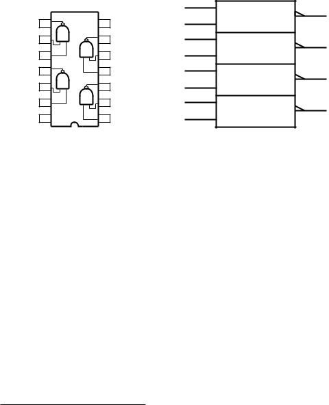
Fig. 2.1 The 74LS00 quad 2-I/P NAND package.
The 74LS001 comprises four 2-input NAND gates in a 14-pin package. The integrated circuit (IC) is powered with a 5 ± 0.25 V supply between VCC2 (usually about 5 V) and GND.The logic outputs are 2.4 – 5 V High and 0 – 0.4 V for Low. Most IC logic families require a 5 V supply, but 3 V versions are becoming available, and some CMOS implementations can operate with a range of supplies between 3 V and 15 V.
The 74LS00 IC is shown in Fig. 2.1(a) in its Dual In-Line (DIL) package. Strictly it should be described as a positive-logic quad 2-I/P NAND, as the electrical equivalent for the two logic levels 0 and 1 are Low (L is around ground potential) and High (H is around Vcc,3 usually about 5 V). If the relationship 0 → H; 1 → L is used (negative logic) then the 74LS00 is actually a quad 2-I/P NOR gate. The ANSI/IEC4 logic symbol of Fig. 2.1(b) denotes a Low electrical potential by using the polarity  symbol. The ANSI/IEC NAND symbol shown is thus based on the real electrical operation of the circuit. In this case the logic coincides with a
1The LS stands for “Low-power Schottky transistor”. There are very many other versions, such as ALS (Advanced LS), AS (Advanced Schottky) and HC (High-speed Complementary metal-oxide transistor – CMOS). These family variants di er in speed and power consumption, but for a given number designation have the same logic function and pinout.
2For historical reasons the positive supply on logic ICs are usually designated as VCC; the C referring to a bipolar’s transistor Collector supply. Similarily field-e ect circuitry sometimes use the designation VDD for Drain voltage. The zero reference pin is normally designated as the ground point (GND), but sometimes the VEE (for emitter) or VSS (for Drain) label is employed.
3For historical reasons the positive supply on logic ICs are usually designated as VCC; the C referring to a bipolar’s transistor Collector supply. Similarily field-e ect circuitry sometimes use the designation VDD for Drain voltage. The zero reference pin is normally designated as the ground point (GND), but sometimes the VEE (for emitter) or VSS (for Drain) label is employed.
4The American National Standards Institution/International Electrotechnical Commission.
2. Logic Circuitry 19
positive-logic NAND function. The & operator shown in the top block is assumed applicable to the three lower gates.
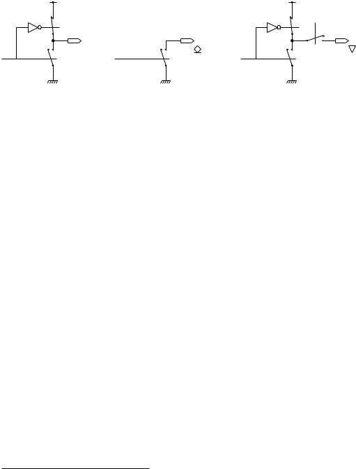
The output structure of a 74LS00 NAND gate is active pull-up. Here both the High and Low states are generated by connection via a lowresistance switch to Vcc or GND respectively. In Fig. 2.2(a) these switches are shown for simplicity as metallic contacts, but they are of course transistor derived.
+Vcc |
|
+Vcc |
|
Phase splitter |
|
Phase splitter |
EN |
|
|
|
|
High/Low |
Off/Low |
|
High/Low/Off |
Internal logic state |
Internal logic state |
Internal logic state |
|
(a) Push/pull (Totem-pole) |
(b) Open-collector (open-drain) |
(c) Three-state |
|
Fig. 2.2 Output structures.
Logic circuits, such as the 74LS00, change output state in around 10 nanoseconds.5 To be able to do this, the capacitance of any interconnecting conductors and other logic circuits’ inputs must be rapidly discharged. Mainly for this reason, active pull-up (sometimes called totem-pole) outputs are used by most logic circuits. There are certain circumstances where alternative output structures have some advantages. The open-collector (or open-drain) configuration of Fig. 2.2(b) provides a ‘hard’ Low state, but the High state is in fact an open-circuit. The Highstate voltage can be generated by connecting an external resistor to either Vcc or indeed to a di erent power rail. Non-orthodox devices, such as relays, lamps or light-emitting diodes, can replace this pull-up resistor. The output transistor is often rated with a higher than usual current and/or voltage rating for such purposes.
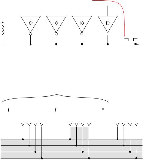
The application of most interest to us here is illustrated in Fig. 2.3. Here four open-collector gates share a single pull-up resistor. Note the use of the  symbol to denote an open-collector output. Assume that there are four peripheral devices, any of which may wish to attract the attention of the processor (eg. computer or microprocessor). If this processor has only one Attention pin, then the four Signal lines must be wire-ORed together as shown. With all Signals inactive (logic 0) the outputs of all bu er NOT gates are o (state H), and the party line is pulled up to +V by RL. If any Signal line is activated (logic 1), as in Sig_1, then the output of the corresponding bu er gate goes hard Low. This pulls
5A nanosecond is 10−9 s, so 100,000,000 transitions each second is possible.
20 The Quintessential PIC Microcontroller
3Sig |
2Sig |
1Sig |
|
0 |
|
|
|||||
|
|
1 |
|||
0 |
0 |
|
|
||
|
|
|
|
||
|
|
0 |
|||
|
|
|
|
||
|
|
|
|
||
|
|
|
|
|
|
+V
RL
Off |
Off |
Off/0/Off |
0_Sig
0
 Off
Off
To processor
Fig. 2.3 Open-collector bu ers driving a party line.
the party line Low, irrespective of the state of the other signal lines, and thus interrupts the processor.
From master controller
Select_0 |
|
Select_1 |
|
Select_2 |
|
||||||
|
0 |
|
|
|
1 |
|
|
|
0 |
|
|
|
EN |
|
|
EN |
|
|
EN |
|
|||
OFF |
Thing 0 |
|
ON |
Thing 1 |
OFF |
Thing 2 |
|||||
|
|
|
|
||||||||
|
|
|
|
|
|
|
|||||
|
|
|
|
|
|
|
|
|
|
|
|
Data bus
d00 d01 d02 d03 |
d10 d11 d12 d13 |
d20 d21 d22 d23 |
 d10
d10
 d11
d11
 d12
d12
 d13
d13
master To
Fig. 2.4 Sharing a bus.
The three-state structure of Fig. 2.2(c) has the properties of both the preceeding output structures. When enabled, the two logic states are represented in the usual way by high and low voltages. When disabled, the output is open circuit irrespective of the activities of the internal logic circuitry and any change in input state. A logic output with this three-state is indicated by the  symbol.
As an example of the use of this structure, consider the situation depicted in Fig. 2.4. Here a master controller wishes to read one of several devices, all connected to this master over a set of party lines. As this data highway or Data bus is a common resource, so only the selected device can be allowed access to the bus at any one time. The access has to be withdrawn immediately the data has been read, so that another device
2. Logic Circuitry 21
can use the resource. As shown in the diagram, each Thing connected to the bus outputs, designated by the  symbol. When selected, only the active logic levels will drive the bus lines. The 74LS244 octal (×8) 3- state (sometimes called tri-state or TRIS) bu er has high-current outputs (designated by the
  symbol) specifically designed to charge/discharge the capacitance associated with long bus lines.
Integrated circuits with a complexity of up to 12 gates are categorised as Small-Scale Integration (SSI). Gate counts upwards to 100 on a single IC are Medium-Scale Integration (MSI), up to 1000 are known as LargeScale Integration (LSI) and over this, Very Large-Scale Integration (VLSI). Memory chips and microprocessors are examples of this latter category.
|
|
|
|
|
|
|
X/Y |
|
|
|
|
B |
|
|
|
|
|
[1/2 x 74LS139] |
|
|
|||
|
|
|
G |
(1,15) |
|
|
|
|
(9,7) |
Y |
|
|
|
|
|
EN |
|
|
|
||||
|
|
|
|
|
|
|
3 |
3 |
|||
|
|
|
|
|
|
|
|
|
|
(6,10) Y |
|
|
|
|
|
|
|
|
|
|
2 |
2 |
|
A |
|
|
|
|
|
|
|
|
1 |
(5,11) Y |
|
|
|
|
|
|
|
|
|
|
|
1 |
|
G |
|
|
|
B |
(3,13) |
1 |
|
|
0 |
(4,12) Y |
|
|
|
|
|
|
|
|
0 |
||||
|
|
|
|
A |
(2,14) |
0 |
|
|
|
|
|
|
|
|
|
|
G B A Y0 Y1 Y2 Y3 |
|
|||||
Y0 |
Y1 |
Y2 |
Y3 |
|
0 |
0 0 |
0 |
1 |
1 |
1 |
|
|
0 0 1 1 0 1 1 |
|
|||||||||
(a) The 74LS139 dual 2- to 4-line decoder. |
|
|
0 |
1 0 |
1 |
1 |
0 |
1 |
|
||
|
|
0 |
1 1 |
1 |
1 |
1 |
0 |
|
|||
|
|
|
|
|
|
||||||
|
|
|
|
|
1 |
X X |
1 |
1 |
1 |
1 |
|
|
|
|
|
X/Y |
|
|
|
|
|
|
|
|
|
|
|
|
|
|
|
|
|
|
|
|
|
[74LS138] |
7 |
(7) |
Y7 |
EN C B A |
|
Y0 Y1 Y2 Y3 Y4 Y5 Y6 Y7 |
|||||||||||||
|
|
|
|
|||||||||||||||||||
|
|
(5) |
& |
|
|
(9) |
Y |
|
|
|
|
|
|
|
|
|
|
|
|
|
|
|
|
|
|
|
|
|
|
|
|
|
|
|
|
|
|
|
|
|
|||||
G2B |
|
6 |
0 |
0 0 0 |
|
0 |
1 |
1 |
1 |
1 |
1 |
1 |
1 |
|
||||||||
|
|
|
6 |
|
|
|||||||||||||||||
(4) |
||||||||||||||||||||||
|
|
|
|
|
|
|
|
|
|
|
|
|
|
|
|
|
|
|
|
|
||
|
|
|
|
|
(10) Y5 |
0 |
0 0 1 |
|
1 |
0 |
1 |
1 |
1 |
1 |
1 |
1 |
|
|||||
G2A |
|
EN |
5 |
|
|
|||||||||||||||||
|
|
|
|
|||||||||||||||||||
G1 |
(6) |
|
|
4 |
(11) |
Y |
|
0 |
0 1 0 |
|
1 |
1 |
0 |
1 |
1 |
1 |
1 |
1 |
|
|||
|
|
|
|
|||||||||||||||||||
|
|
|
|
|
|
|
4 |
0 |
0 1 1 |
|
1 1 1 0 1 1 1 1 |
|
||||||||||
|
|
|
|
|
|
|
|
|
|
|
||||||||||||
|
|
|
|
|
3 |
(12) Y |
||||||||||||||||
|
|
|
|
|
|
|
3 |
0 |
1 0 0 |
|
1 1 1 1 0 1 1 1 |
|
||||||||||
|
|
|
|
|
|
|
|
|
||||||||||||||
|
|
(3) |
|
|
|
(13) Y |
||||||||||||||||
C |
2 |
|
2 |
0 |
1 0 1 |
|
1 1 1 1 1 0 1 1 |
|
||||||||||||||
|
|
|
2 |
|
|
|||||||||||||||||
|
|
|||||||||||||||||||||
B |
(2) |
1 |
|
1 |
(14) |
Y |
|
0 |
1 1 0 |
|
1 |
1 |
1 |
1 |
1 |
1 |
0 |
1 |
|
|||
|
|
|
1 |
0 |
1 1 1 |
|
1 |
1 |
1 |
1 |
1 |
1 |
1 |
0 |
|
|||||||
A |
(1) |
0 |
|
0 |
(15) |
Y |
|
|
|
|||||||||||||
|
|
|
0 |
1 |
X X X |
|
1 1 1 1 1 1 1 1 |
|||||||||||||||
|
|
|
|
|
|
|
|
|
|
|||||||||||||
|
|
|
|
|
|
|
|
|
||||||||||||||
|
|
|
|
|
|
|
|
|
|
|
|
|
|
|
|
|
|
|
|
|
|
|
(b) The 74LS138 3- to 8-line decoder
Fig. 2.5 The 74LS138 and ’139 MSI natural decoders.

22 The Quintessential PIC Microcontroller
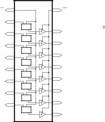
The NAND gate networks shown in Fig. 2.5 are typical MSI-complexity ICs. Remembering that the output of a NAND gate is logic 0 only when all its inputs are logic 1 (see Fig. 1.2(c) on page 13) then we see that for any combination of the Select inputs B A (21 20) in Fig. 2.5(a) only one gate will go to logic 0. Thus output Y2 will be activated when B A = 10. The associated truth table shows the circuit decodes the binary address B A so that address n selects output Yn. The 74LS139 is described as a dual 2 to 4-line natural decoder. Dual because there are two such circuits in the one chip. The symbol X/Y denotes converting code X (natural binary) to code Y (unary – one of n). The Enable input G is connected to all gates in parallel. Thus the decoder function only operates if G is Low (logic 0). If G is High, then irrespective of the state of B A (the X entries in the truth table denote a ‘don’t care’ situation) all outputs remain deselected – logic 1. An example of the use of the 74LS139 is given in Fig. 2.23.
The 74LS138 of Fig. 2.5(b) is similar, but implements a 3 to 8-line decoder function. The state of the three address lines C B A (22 21 20) n selects one only of the eight outputs Yn. The 74LS138 has three Gate inputs which generate an internal Enable signal G2B · G2A · G1. Only if both G2A and G2B are Low and G1 is High will the device be enabled. The 74LS138 is used in Fig 11.10 on page 287 to decode microcontroller port lines to enable several devices to communicate to the one port.
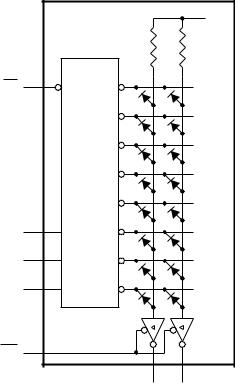
A large class of ICs implement arithmetic operations. The gate array illustrated in Fig. 2.6 detects when the 8-bit byte P7…P0 is identical to the byte Q7…Q0. Eight ENOR gates each give a logic 1 when its two input bits Pn, Qn are identical, as described on page 14. Only if all eight bit pairs are the same, will the output NAND gate go Low. The 74LS688 Equality comparator also has a direct input G into this NAND gate, acting as an overall Enable signal.
The ANSI/IEC logic symbol, shown in Fig. 2.6(b) uses the COMP label to denote the arithmetic comparator function. The output is prefixed with the numeral 1, indicating that its operation P=Q is dependent on any input qualifying the same numeral; that is G1. Thus the active-Low Enable input G1 gates the active-Low output, 1P=Q.
One of the first functions beyond simple gates to be integrated into a single IC was that of addition. The truth table of Fig. 2.7(a) shows the Sum (S) and Carry-Out (C1) resulting from the addition of the two bits A and B and any Carry-In (C0). For instance row 6 states that adding two 1s with a Carry-In of 0 gives a Sum of 0 and a Carry-Out of 1 (1 + 1 + 0 =10). To im- plement this row we require to detect the pattern 1 1 0; that is A · B · C0; which is gate 6 in the logic diagram. Thus we have by ORing all applicable patterns together for each output:
S= (A · B · C0) + (A · B · C0) + (A · B · C0) + (A · B · C0)
C1 = (A · B · C0) + (A · B · C0) + (A · B · C0) + (A · B · C0)

|
|
|
|
2. |
Logic Circuitry |
23 |
|
P7 |
(17) |
P7=Q7 |
|
|
|
|
|
|
|
|
[74LS688] |
|
|
||
Q7 |
(18) |
|
|
|
|
|
|
|
|
|
|
|
|
|
|
|
|
|
|
1 |
|
|
|
P6 |
(15) |
P6=Q6 |
|
|
G1 |
|
|
(16) |
|
|
|
|
|||
Q6 |
|
|
|
|
|
|
|
|
|
|
|
|
|
|
|
P5 |
(13) |
P5=Q5 |
|
17 |
7 |
|
|
|
15 |
|
|
|
|||
(14) |
|
|
|
|
|||
Q5 |
|
|
|
|
|
|
|
|
|
|
13 |
|
|
|
|
P4 |
(11) |
P4=Q4 |
|
11 |
|
|
|
|
|
|
|
|
|||
(12) |
|
8 |
P |
|
|
||
Q4 |
|
|
|
|
|||
|
(19) |
P=Q |
|
|
|
|
|
|
|
6 |
|
|
|
||
|
(8) |
|
|
|
|
||
P3 |
P3=Q3 |
|
4 |
|
|
|
|
(9) |
|
|
|
|
|||
Q3 |
|
|
2 |
|
|
|
|
|
|
|
0 |
19 |
|
||
|
|
|
|
|
1P=Q |
|
|
P2 |
(6) |
P2=Q2 |
|
|
|
|
|
(7) |
|
18 |
|
|
|
||
Q2 |
|
|
7 |
|
|
||
|
|
|
|
16 |
|
|
|
P1 |
(4) |
P1=Q1 |
|
14 |
|
|
|
(5) |
|
|
|
|
|||
Q1 |
|
|
12 |
|
|
|
|
|
|
|
|
|
|
||
P0 |
(2) |
P0=Q0 |
|
9 |
Q |
|
|
|
|
|
|
|
|||
(3) |
|
7 |
|
|
|
||
Q0 |
|
|
|
|
|
||
|
|
|
5 |
|
|
|
|
|
|
|
|
|
|
|
|
G |
(1) |
Enable |
|
3 |
0 |
|
|
|
|
|
|
|
|
|
|
(a) Logic function |
(b) ANSI/IEC logic symbol |
Fig. 2.6 The 74LS688 octal equality detector.
Using such a circuit for each column of a binary addition, with the Carry-Out from column k−1 feeding the Carry-In of column k means that the addition of any two n-bit words can be simultaneously implemented. As shown in Fig. 2.7(b), the 74LS283 adds two 4-bit nybbles in 25 ns. In practice the final Carry-Out C4 is generated using additional circuitry to avoid the delays inherent on the carries rippling though each stage from the least to the most significant digit. n 74LS283s can be cascaded to implement addition for words of 4 × n width. Thus two 74LS283s perform a 16-bit addition in 45 ns; the extra time being accounted for by the carry propagation between the two units.
Adders can of course be coaxed into subtraction by inverting the minuend and adding one, that is 2’s complementation. An Adder/Subtractor circuit could be constructed by feeding the minuend word through an array of XOR gates acting as programmable inverters (see page 14). The Mode line Add/Sub in Fig. 2.8 that controls these inverters also feeds the Carry-In, e ectively adding one when in the Subtract mode.
Extending this line of argument leads to the Arithmetic Logic Unit (ALU). An ALU is a circuit which can undertake a selection of arithmetic and logic processes on input data as controlled by Mode inputs. The 74LS382 in Fig. 2.9 processes two 4-bit operands in eight ways, as controlled by the three Select bits S2 S1 S0 and tabulated in Fig. 2.9(a). Besides

24 The Quintessential PIC Microcontroller
|
|
A B C0 |
|
|
S C1 |
|
|
|
|
|
|
|
|
|
|
|
|
|
|
|
|
|
|
|
|
|
|
|
|
|
|
|
|
|
|
|
|
|
|
|||||||||
|
|
|
|
|
|
|
|
|
|
|
|
|
|
|
|
|
A |
|
|
|
|
|
|
|
|
1 |
|
|
|
|
|
|
|
|
|
|
|
|
|
|
|
|
|
|
|
|
|
|
|
|
|
|
|
|
|
|
|
|
|
|
|
|
|
|
|
|
|
|
|
|
|
|
|
|
|
|
|
|
|
|
|
|
|
|
|
|
|
|
|
|
|||||||
|
|
|
|
|
|
|
|
|
|
|
|
|
|
|
|
|
B |
|
|
|
|
|
|
|
|
|
|
|
|
|
|
|
|
|
|
|
|
|
|
|
|
|
|
|
||||
0 |
0 0 0 |
|
|
0 0 |
|
|
|
|
|
C0 |
|
|
|
|
|
|
|
|
|
|
|
|
|
|
|
|
|
|
|
|
|
|
|
|
|
|
|
|
||||||||||
|
|
|
|
|
|
|
|
|
|
|
|
|
|
|
|
|
|
|
|
|
|
|
|
|
|
|
|
|
|
|
|
|
||||||||||||||||
1 |
0 0 1 |
|
|
1 0 |
|
|
|
|
|
|
|
|
|
|
|
|
|
|
|
|
|
|
|
|
|
|
|
|
|
|
|
|
|
|
|
|
|
|
|
|
||||||||
|
|
|
|
|
A |
|
|
|
2 |
|
|
|
|
|
|
|
|
|
|
|
|
|
|
|
|
|
|
|
|
|
|
|||||||||||||||||
|
|
|
|
|
|
|
|
|
|
|
|
|
|
|
|
|
|
|
|
|
|
|
|
|
|
|
|
|
|
|
|
|
|
|
|
|
||||||||||||
2 |
0 1 0 |
|
|
1 0 |
|
|
|
|
|
|
B |
|
|
|
|
|
|
|
|
|
|
|
|
|
|
|
|
|
|
|
S |
|
|
|
|
|
|
|
||||||||||
3 |
0 1 1 |
|
|
0 1 |
|
|
|
|
|
C0 |
|
|
|
|
|
|
|
|
|
|
|
|
|
|
|
|
|
|
|
|
|
|
|
|
||||||||||||||
4 |
1 0 0 |
|
|
1 0 |
|
|
|
|
|
A |
|
|
|
|
|
|
|
|
|
|
|
|
|
|
|
|
|
|
Sum out |
|
|
|
|
|
|
|||||||||||||
|
|
|
|
|
|
|
|
B |
|
|
|
|
|
|
|
4 |
|
|
|
|
|
|
|
|
1 + 2 + 4 + 7 |
|
|
|
|
|
|
|
|
|||||||||||||||
5 |
1 0 1 |
|
|
0 1 |
|
|
|
|
|
|
|
|
|
|
|
|
|
|
|
|
|
|
|
|
|
|
|
|
|
|
|
|
||||||||||||||||
|
|
|
|
|
|
|
C0 |
|
|
|
|
|
|
|
|
|
|
|
|
|
|
|
|
|
|
|||||||||||||||||||||||
|
|
|
|
|
|
|
|
|
|
|
|
|
|
|
|
|
|
|
|
|
|
|
|
|
|
|
|
|
|
|
|
|
|
|
||||||||||||||
6 |
1 1 0 |
|
|
0 1 |
|
|
|
|
|
A |
|
|
|
|
|
|
|
|
|
|
|
|
|
|
|
|
|
|
|
|
|
|
|
|
|
|
|
|
||||||||||
7 |
1 1 1 |
|
|
1 1 |
|
|
|
|
|
|
|
|
|
|
7 |
|
|
|
|
|
|
|
|
|
|
|
|
|
|
|
|
|
|
|
|
|
|
|||||||||||
|
|
|
|
|
|
|
|
B |
|
|
|
|
|
|
|
|
|
|
|
|
|
|
|
|
|
|
|
|
|
|
|
|
|
|
|
|||||||||||||
|
|
|
|
|
|
|
|
|
|
|
|
|
|
|
|
|
|
|
|
|
|
|
|
|
|
|
|
|
|
|
|
|
||||||||||||||||
|
|
|
|
|
|
|
|
|
|
|
|
|
|
|
|
C0 |
|
|
|
|
|
|
|
|
|
|
|
|
|
|
|
|
|
|
|
|
|
|
|
|
|
|
|
|
||||
|
|
|
|
|
|
|
|
|
|
|
|
|
|
|
|
|
|
|
|
|
|
|
|
|
|
|
|
|
|
|
|
|
|
|
|
|
|
|
|
|
|
|
||||||
|
|
|
|
|
|
|
|
|
|
|
|
|
|
|
|
A |
|
|
|
|
|
5 |
|
|
|
|
|
|
|
|
|
|
|
|
|
|
|
|
|
|
|
|
|
|
||||
|
|
|
|
|
|
|
|
|
|
|
|
|
|
|
|
|
|
|
|
|
|
|
|
|
|
|
|
|
|
|
|
|
|
|
|
|
|
|
|
|
|
|||||||
|
|
|
|
|
|
|
|
|
|
|
|
|
|
|
|
|
B |
|
|
|
|
|
|
|
|
|
|
|
|
|
|
|
|
|
C |
|
|
|
|
|
|
|||||||
|
|
|
|
|
|
|
|
|
|
|
|
|
|
|
|
C0 |
|
|
|
|
|
|
|
|
|
|
|
|
|
|
|
|
|
|
|
|
|
|
|
|
||||||||
|
|
|
|
|
|
|
|
|
|
|
|
|
|
|
|
|
|
|
|
|
|
|
|
|
|
|
|
|
|
|
|
|
|
|
|
|
|
|||||||||||
|
|
|
|
|
|
|
|
|
|
|
|
|
|
|
|
|
|
|
|
|
|
|
|
|
|
|
|
|
|
|
|
|
|
|
|
|
|
|||||||||||
|
|
|
|
|
|
|
|
|
|
|
|
|
|
|
|
|
|
|
|
|
|
|
|
|
|
|
|
|
|
|
|
|
|
|
|
|
|
1 |
|
|
|
|
|
|
|
|
|
|
|
|
|
|
|
|
|
|
|
|
|
|
|
|
|
|
|
|
|
|
|
|
|
|
|
|
|
|
|
|
|
|
|
|
|
|
|
|
|
|
|
|
|
|
|
|
|
|
|
|
|
|
|
|
|
|
|
|
|
|
|
|
|
|
|
A |
|
|
|
|
|
6 |
|
|
|
|
|
|
|
|
|
|
|
|
Carry out |
|
|
|
|
|||||||||
|
|
|
|
|
|
|
|
|
|
|
|
|
|
|
|
|
B |
|
|
|
|
|
|
|
|
|
|
|
|
|
3 + 5 + 6 + 7 |
|
|
|
|
|
|
|
|
|||||||||
|
|
|
|
|
|
|
|
|
|
|
|
|
|
|
|
|
|
|
|
|
|
|
|
|
|
|
|
|
|
|
|
|
|
|
|
|
||||||||||||
|
|
|
|
|
|
|
|
|
|
|
|
|
|
|
|
|
|
|
|
|
|
|
|
|
|
|
|
|
|
|
|
|
|
|
|
|
|
|
|
|
|
|
||||||
|
|
|
|
|
|
|
|
|
|
|
|
|
|
|
|
C0 |
|
|
|
|
|
|
|
|
|
|
|
|
|
|
|
|
|
|
|
|
||||||||||||
|
|
|
|
|
|
|
|
|
|
|
|
|
|
|
|
|
|
|
|
|
|
|
|
|
|
|
|
|
|
|
|
|
|
|
|
|
|
|
|
|
|
|
|
|||||
|
|
|
|
|
|
|
|
|
|
|
|
|
|
|
|
|
A |
|
|
|
|
|
|
3 |
|
|
|
|
|
|
|
|
|
|
|
|
|
|
|
|
|
|
|
|
|
|
||
|
|
|
|
|
|
|
|
|
|
|
|
|
|
|
|
|
|
|
|
|
|
|
|
|
|
|
|
|
|
|
|
|
|
|
|
|
|
|
|
|
|
|
|
|
|
|
||
(a) One-bit addition |
|
|
|
|
|
|
|
B |
|
|
|
|
|
|
|
|
|
|
|
|
|
|
|
|
|
|
|
|
|
|
|
|
|
|
|
|||||||||||||
|
|
|
|
|
|
|
|
|
|
|
|
|
|
|
|
|
|
|
|
|
|
|
|
|
|
|
|
|
|
|
|
|
||||||||||||||||
|
|
|
|
|
|
C0 |
|
|
|
|
|
|
|
|
|
|
|
|
|
|
|
|
|
|
|
|
|
|
|
|
|
|
|
|
||||||||||||||
|
|
|
|
|
|
|
|
|
|
|
|
|
|
|
|
|
|
|
|
|
|
|
|
|
|
|
|
|
|
|
|
|
||||||||||||||||
|
|
|
|
|
|
B4 |
A4 |
|
|
B3 |
A3 |
|
|
|
|
B2 |
|
A2 |
|
|
B1 |
A1 |
|
|
|
|
||||||||||||||||||||||
|
|
|
|
|
|
|
|
(11) |
|
(12) |
|
|
(15) |
|
(14) |
|
|
(2) |
|
|
(3) |
|
|
(6) |
|
|
(5) |
|
|
|
|
|||||||||||||||||
|
|
|
|
|
|
|
|
|
|
|
|
|
|
|
|
|
|
|
|
|
|
|
|
|
|
|
|
|
|
|
|
|
|
|
|
|
|
|
|
|
|
|
|
|
|
|
|
|
|
|
|
|
|
|
|
|
|
|
|
|
|
|
|
|
|
|
|
|
|
|
|
|
|
|
|
|
|
|
|
|
|
|
|
|
|
|
|
|
|
|
|
|
|
|
|
|
|
Carry-out |
|
|
|
B |
|
|
A |
|
|
|
B |
A |
|
|
|
|
B |
|
A |
|
|
|
|
|
B |
A |
|
|
Carry-in |
|||||||||||||||||||
|
|
C1 |
|
|
|
|
|
|
C0 |
|
|
C1 |
|
|
|
C0 |
|
|
C1 |
|
|
|
|
C0 |
|
|
C1 |
|
C0 |
|
|
|||||||||||||||||
C4 |
(9) |
|
|
|
|
|
|
|
|
|
|
|
|
|
|
|
|
|
|
|
|
|
|
|
|
(7) |
C0 |
|||||||||||||||||||||
|
|
|
|
|
S |
|
|
|
|
|
|
|
|
|
|
|
S |
|
|
|
|
|
|
|
|
|
S |
|
|
|
|
|
|
S |
|
|
|
|
||||||||||
|
|
|
|
|
|
|
|
|
|
|
|
|
|
|
|
|
|
|
|
|
|
|
|
|
|
|
|
|
|
|
|
|
|
|
|
|
|
|||||||||||
|
|
|
|
|
|
|
|
|
|
|
|
|
|
|
|
|
|
|
|
|
|
|
|
|
|
|
|
|
|
|
|
|
|
|||||||||||||||
|
|
|
|
|
|
|
|
|
|
|
|
|
|
|
|
|
|
|
|
|
|
|
|
|
|
|
|
|
|
|
|
|
|
|
|
|
|
|
|
|
|
|
|
|
|
|
|
|
|
|
|
|
|
|
|
|
|
(10) |
|
|
|
|
|
|
|
|
|
(13) |
|
|
|
|
|
|
|
|
(1) |
|
|
|
|
|
|
|
|
(4) |
|
|
|
|
|
||||||
|
|
|
|
|
|
|
|
S4 |
|
|
|
|
|
|
|
|
|
|
|
S3 |
|
|
|
|
|
|
|
|
|
S2 |
|
|
|
|
|
|
S1 |
|
|
|
|
|
|
|||||
(b) The 74LS283 four-bit adder
Fig. 2.7 Addition.
addition and subtraction, the logic operations of AND, OR and XOR are supported. The 74LS382 even generates the 2’s complement overflow function (see page 10).
As we shall see, the ALU is the heart of the computer and microprocessor architectures. By feeding the Select inputs with a series of mode words, a program of operations can be performed by the ALU. Such operation codes are stored in an external memory, and are accessed sequentially by the computer’s control circuits.
Sequences of program operation codes are normally stored in an LSI Read-Only Memory (ROM). Consider the architecture illustrated in Fig. 2.10. This is essentially a 3 to 8-line decoder driving an 8 × 2 array of diodes. The 3-bit address selects only row n for each input combination n. If a diode is connected to this row, then it conducts and brings the appropriate column Low. The inverting 3-state output bu er consequently gives a High for each connected diode and Low where the link is broken. The pattern of diode links then defines the output code for each input. For illustrative purposes, the structure has been programmed to

2. Logic Circuitry 25
Word A |
Word B |
ADD/SUB
A4 A3 A2 |
A1 |
B4 |
B3 B2 B1 |
C4 |
|
|
C0 |
S4 |
S3 |
S2 |
S1 |
Carry/Borrow out |
Sum/Difference |
Fig. 2.8 Implementing a programmable adder/subtractor.
S2S1S0 |
|
Operation |
|
|
|
|
Word A |
|
|
Word B |
Mode Select S |
|
Carry-In |
||||||||||||||||||||||||||
|
|
||||||||||||||||||||||||||||||||||||||
|
|
|
|
|
|
|
|
|
|
|
|
|
|
|
|
|
|
|
|
|
|
|
|
|
|
|
|
|
|
|
|
|
|
|
|
|
|
||
0 |
0 |
0 |
|
Clear |
(F=0000) |
|
|
|
|
|
|
|
|
|
|
|
|
|
|
|
|
|
|
|
|
|
|
|
|
|
|
|
|
|
|||||
|
|
|
|
|
|
|
|
|
|
|
|
|
|
|
|
|
|
|
|
|
|
|
|
|
|
|
|
|
|
|
|
|
|||||||
0 |
0 |
1 |
|
Subtract |
(B-A) |
|
|
|
|
|
|
|
|
|
|
|
|
|
|
|
|
|
|
|
|
|
|
|
|
|
|
|
|
|
|
|
|
||
0 |
1 |
0 |
|
Subtract |
(A-B) |
(17) (19) (1) (3) |
(16) (18) |
(2) |
|
(4) |
(7) |
(6) |
(5) |
(15) |
|
||||||||||||||||||||||||
0 |
1 |
1 |
|
Add |
|
(A+B) |
|
|
A3 |
A2 |
A1 A0 |
B3 |
B2 |
B1 |
B0 |
|
S2 |
|
S1 |
|
S0 |
C(n) |
|
||||||||||||||||
1 |
0 |
0 |
|
EOR |
|
(A + B) |
|
|
|
|
|
|
|||||||||||||||||||||||||||
|
|
|
|
|
|
|
|
|
|
|
|
|
|
|
|
|
|
|
|
|
|
|
|
|
|
|
|
|
|
|
|
|
|
||||||
1 |
0 |
1 |
|
OR |
|
(A + B) |
|
|
|
|
|
|
|
|
|
|
|
|
|
|
|
ALU |
|
|
|
|
|
|
|
|
|
|
|
|
|
|
|
||
1 |
1 |
0 |
|
AND |
|
(A B) |
|
|
|
|
|
|
|
|
|
|
|
|
|
[74LS382] |
|
|
|
|
|
|
|
|
|
|
|
||||||||
1 |
1 |
1 |
|
Preset |
(F=1111) |
|
|
|
|
|
|
|
|
C(n+4) |
OVR |
|
|
|
|
F3 F2 F1 |
F0 |
|
|
|
|||||||||||||||
|
|
|
|
|
|
|
|
|
|
|
|
|
|
|
|
|
|
|
|
|
|
|
|||||||||||||||||
|
|
|
|
|
|
|
|
|
|
|
|
|
|
|
|
|
|
|
|
|
|
|
|
|
|
|
|
|
|
|
|
|
|
|
|
|
|
|
|
|
|
|
|
|
|
|
|
|
|
|
|
|
|
|
|
(14) |
|
|
(13) |
|
|
|
|
|
(12) |
(11) |
(9) |
|
(8) |
|
|
|
|||||||
|
|
|
|
|
|
|
|
|
|
|
|
|
|
|
|
|
|
|
|
|
|
|
|
|
|
|
|
|
|
|
|
|
|
|
|||||
|
|
|
|
|
|
|
|
|
|
Carry-Out |
|
|
|
|
|
|
|
|
|
|
|
|
|
|
|
|
|
|
|
|
|
|
|||||||
|
|
|
|
|
|
|
|
|
|
|
|
|
|
|
Function Output F |
||||||||||||||||||||||||
|
|
|
|
|
|
|
|
|
|
|
|
|
|
|
|
|
Overflow |
||||||||||||||||||||||
(a) |
Function table |
|
|
(b) |
Logic diagram/pinning |
|
|
|
|
|
|
|
|
|
|
|
|
|
|
|
|
||||||||||||||||||
Fig. 2.9 The 74LS382 ALU.
implement the 1-bit full adder of Fig. 2.7(a), but any two functions of three variables can be generated.
The diode matrix look-up table shown here is known as a Read-Only Memory (ROM), as its ‘memory’ is in the diode pattern, which is programmed in when the device is manufactured. Early devices, which were typically decoder/32 × 8 matrices, usually came in user-programmable versions in which the links were implemented with fusible links. By using
26 The Quintessential PIC Microcontroller
 +V
+V
Chip Select |
|
|
X/Y |
1 |
|
|
CS |
0 |
G |
0 |
|
|
|
|
|
|
1 1 |
|
|
|
|
|
|
2 1 |
|
|
|
|
|
|
3 1 |
|
|
|
Address |
|
|
4 |
1 |
|
|
1 |
|
5 0 |
|
|
||
A |
4 |
|
|
|||
B |
0 |
2 |
6 |
1 |
1 |
0 |
|
|
|||||
C0 |
1 |
1 |
7 |
1 |
|
|
|
|
|
||||
|
|
|
|
|||
Output Enable |
|
|
|
|
|
|
OE |
0 |
|
|
|
|
|
|
|
|
|
|
0 |
1 |
|
|
|
|
|
S |
C1 Output data |
Fig. 2.10 A ROM-implemented 1-bit adder.
a high voltage, a selection of diodes could be taken out of contact. Such devices are called Programmable ROMs (PROMs).
Fuses are messy when implementing the larger sizes of VLSI PROM necessary to store computer programs. For example, the 27C64 PROM shown in Fig. 2.11 has the equivalent of 65,536 fuse/diode pairs, and this is a relatively small device capable of storing 8192 bytes of memory. The 27C64 uses electrical charge on the floating gate of a metal-oxide field-e ect transistor (MOSFET) as the programmable link, with another MOSFET to replace the diode. Charge can be tunnelled onto this isolated gate by, again, using a high voltage. Once on the gate, the electric field keeps the link MOSFET conducting. This charge takes many decades to leak away, but this can be dramatically reduced to about 30 minutes by exposure to intensive ultra-violet radiation. For this reason the 27C64 is known as an Erasable PROM (EPROM). When an EPROM is designed for reusability, a quartz window is integrated into the package, as shown in Fig. 2.11. Programming is normally done externally with special equipment, known as PROM programmers, or colloquially as PROM blasters. Versions without windows are referred to as One-Time Programmable (OTP) ROMs, as they cannot easily be erased once programmed. They
|
|
|
|
|
|
2. |
Logic Circuitry |
27 |
VPP |
1 |
28 |
VDD |
|
EPROM |
8192x8 |
|
|
A0 |
0 |
[2764] |
|
|||||
A12 2 |
27 |
PGM |
|
|||||
A1 |
|
|
|
|
||||
|
|
|
|
|
|
|
|
|
A7 |
3 |
26 |
|
A2 |
|
|
A |
D0 |
A6 |
4 |
25 |
A8 |
A3 |
|
|
A |
D1 |
A4 |
|
|
A |
D2 |
||||
A5 5 |
24 |
A9 |
|
|
||||
A5 |
|
0 |
A |
D3 |
||||
A4 |
6 |
23 |
A11 |
A6 |
A |
A |
D4 |
|
|
|
|
|
A7 |
|
8191 |
A |
D5 |
A3 7 |
22 |
OE |
|
|
||||
A8 |
|
|
A |
D6 |
||||
A2 8 |
21 A10 |
|
|
|||||
A9 |
|
|
A |
D7 |
||||
A1 9 |
20 |
CE |
A10 |
|
|
|
|
|
A0 10 |
19 |
D7 |
A11 |
|
|
|
|
|
A12 |
12 |
|
|
|
||||
D0 11 |
18 |
D6 |
|
|
|
|||
|
|
|
|
|
||||
D1 12 |
17 |
D5 |
CS |
[POWER DOWN] |
|
|||
D2 13 |
16 |
D4 |
|
& |
|
|
|
|
|
EN |
|
|
|||||
VSS 14 |
15 |
D3 |
|
|
|
|||
OE |
|
|
|
|
||||
|
|
|
|
|
|
|
|
|
(a) |
Dual in-line package |
|
|
(b) |
Logic symbol |
|
|
|
Fig. 2.11 The 2764 Erasable PROM.
are however, much cheaper to produce and are thus suitable for small to medium-scale production runs.
X
VDD
VPP |
|
|
|
Y |
TR2 |
|
G22 |
|
|
|
|
|
||
|
|
G21 |
TR1 |
|
|
|
|
|
|
D2 |
S2 |
|
D1 |
G1 |
Programmable |
Addressable |
S1 |
||
|
||||
element |
|
switch |
||
|
|
|||
|
|
|
|
|
Fig. 2.12 Floating-gate MOSFET link

28 The Quintessential PIC Microcontroller
Figure 2.12 shows a simplified representation of such a floating-gate MOSFET link. The cross-point device is a metal-oxide enhancement n- channel field-e ect transistor TR1, rather than a diode. This MOSFET has its gate G1 connected to the X line and its source S1 to the Y line. If its drain D1 were connected to the positive supply and the X line is selected (positive), then the Y line too becomes positive (positive-logic 1) as TR1 is conducting (switch is on). However, if TR1 is disconnected from VDD then it does not conduct and the output on the Y line is logic 0. Transistor TR2 is in series with VDD and thus acts as the programmable element. Transistor TR2 has an extra unconnected gate buried in the silicon dioxide insulation layer. Normally there is no charge on this gate and TR2 is o . If the programming voltage VPP is pulsed high to typically 20 – 25 V, negative charges tunnel across the extemely thin insulation surrounding the buried gate. This permanently turns TR2 on and thus connects TR1 to its supply. This shows up as a logic 1 on the Y line when selected by the internal memory decoder.
This charge remains more or less permanently on the buried gate until it is exposed to ultra-violet light. The high-energy light photons knock electrons (negative charges) out of the buried (floating) gate6 e ectively discharging in around 20 minutes and wiping out all stored information. There are PROM structures which can be erased electrically, often in situe in the circuit. These are known variously as Electrically-Erasable PROMs (EEPROMs) or flash memories. In the former case a large negative pulse at VPP causes the captured electrons on the buried gate to tunnel back out. Generally the negative voltage is generated on the chip, which saves having to provide an additional external supply. The flash variant of EEPROM relies on hot electron injection rather than tunneling to charge the floating gate. The geometry of the cell is approximately half the size of a conventional EEPROM cell which increases the memory density. Programming voltages are also somewhat lower.
Most modern EPROM/EEPROMs are fairly fast, taking around 150 ns to access and read. Programming is slow, at perhaps 10 ms per word, but this is an infrequent activity. Flash EEPROM programs around 1000 times faster, in around 10 µs per cell.
All the circuits shown thus far are categorised as combinational logic. They have no memory in the sense that the output simply depends only on the present input, and not the sequence of events leading up to that input. Logic circuits, such as latches, counters, registers and read/write memories are described as sequential logic. Their output not only depends on the current input, but the sequence of prior inputs.
6This is called the Einstein e ect. Einstein was awarded his Nobel prize for this discovery and not for his theories of relativity, as these were considered too revolutionary!

2. Logic Circuitry 29
R S |
Q |
|
|
R |
R |
Q |
|
0 0 |
Q (no change) |
|
|
|
|
|
|
0 1 |
1 |
(set) |
|
|
|
|
|
1 0 |
0 |
(reset) |
|
S |
S |
Q |
|
(a) Defining RS latch truth table |
(b) |
Logic symbol with true/complement outputs |
|||||
0 |
R |
|
0 |
1 |
0 |
|
|
X 1 |
Q |
|
R |
X 0 |
Q |
||
|
X 0 |
|
|
||||
|
|
|
|
|
|
||
0 |
1 0 |
X 0 |
Q |
|
X 0 |
Q |
|
|
|
0 |
X |
1 |
|
|
S |
|
|
S |
|
|
(c) |
Setting the latch |
|
(d) |
Resetting the latch |
|
|
Fig. 2.13 The R S latch.
Consider a typical door bell push-switch. When you press such a switch the bell rings, and it stops as soon as you release it. This switch has no memory.
Compare this with a standard light switch. Set the switch and the light comes on. Moreover it remains on when you remove the stimulus (usually your finger!). To turn the light o you must reset the switch. Again it remains o when the input is taken away. This type of switch is known as a bistable, as it has two stable states. E ectively it is a 1-bit memory cell, that can store either an on or o state indefinitely.
A read-write memory, such as the 6264 device of Fig. 2.24, implements each bistable cell using two cross-coupled transistors. Here we are not concerned with this microscopic view. Instead, consider the two cross-coupled NOR gates of Fig. 2.13. Remembering from Fig. 1.3(c) on page 13 that any logic 1 into a NOR gate will always give a logic 0 output irrespective of the state of the other inputs, allows us to analyse the circuit:
•If the S input goes to 1, then output Q goes to 0. Both inputs to the top gate are now 0 and thus output Q goes to 1. If the S input now goes back to 0, then the lower gate remains 0 (as the Q feedback is 1) and the top gate output also remains unaltered. Thus the latch is set by pulsing the S input.
•If the R input goes to 1, then output Q goes to 0. Both inputs to the bottom gate are now 0 and thus output Q goes to 1. If the R input now goes back to 0, then the upper gate remains 0 (as the Q feedback is 1) and the bottom gate output also remains unaltered. Thus the latch is reset by pulsing the R input.

30 The Quintessential PIC Microcontroller
In the normal course of events – that is assuming that the R and S inputs are not both active at the same time7 then the two outputs are always complements of each other, as indicated by the logic symbol of Fig. 2.13(b).
+V
S
Q
R Q
+V
Fig. 2.14 Using a R S latch to debounce a switch.
There are many bistable implementations. For example, replacing the NOR gates by NAND gives a R S latch, where the inputs are active on a logic 0. The circuit illustrated in Fig. 2.14 shows such a latch used to debounce a mechanical switch. Manual switches are frequently used as inputs to logic circuits. However, most metallic contacts will bounce o the destination contact many times over a period of several tens of milliseconds before settling. For instance, using a mechanical switch to interrupt a computer/microprocessor will give entirely unpredictable results.
In Fig. 2.14, when the switch is moved up and hits the contact the latch is set. When the contact is broken, the latch remains unchanged, provided that the switch does not bounce all the way back to the lower contact. The state will remain Set no matter how many bounces occur. By symmetry, the latch will reset when the switch is moved to the bottom contact, and remain in this Reset state on subsequent bounces.
The D latch is an extension to the R S latch, where the output follows the D (Data) input when the C (Control) input is active (logic 1 in our example) and freezes when C is inactive. The D latch can be considered
7If they where, then both Q and Q go to 0. On relaxing the inputs, the latch will end up in one of its stable states, depending on the relaxation sequence. The response of a latch to a simultaneous Set and Reset is not part of the latch definition, shown in Fig. 2.13(a), but depends on its implementation. For example, trying to turn a light switch on and o together could end in splitting it in two!
2. Logic Circuitry 31
C D |
Q |
|
|
1D |
|
|
|
1 |
0 |
0 |
(transparent) |
|
|
|
|
|
|
|
|||||
|
|
|
|
||||
1 |
1 |
1 |
|
C1 |
|
|
|
0 |
X |
Q (freeze) |
|
|
|
||
|
|
|
|||||
|
|
|
|
||||
(a) |
D latch truth table |
(b) D latch logic diagram |
|||||
C D |
Q |
|
|
|
|
|
|
|
|
1D |
|
|
|||
|
0 |
0 |
(sample) |
|
|
|
|
|
|
|
|||||
|
|
|
|
|
|||
|
1 |
1 |
|
|
C1 |
|
|
0 |
X |
Q |
|
|
|
||
|
|
|
|
|
|||
1 |
X |
Q (hold) |
|
|
|
|
|
XQ
(c) D flip flop truth table |
(d) D flip flop logic diagram |
Fig. 2.15 The D latch and flip flop.
to be a 1-bit memory cell where the datum is retained at its value at the end of the sample pulse.
In Fig. 2.15(b) the dependency of the Data input with its Control is shown by the symbology C1 and 1D. The 1 prefix to D shows that it depends on any signal with a 1 su x, in this case the C input. That is C1 clocks in the 1D data.
A flip flop is also a 1-bit memory cell, but the datum is only sampled on an edge of the control (known here as the Clock) input. The D flip flop
described in Fig. 2.15(c) is triggered on a / |
|
(as illustrated in the truth |
|||||||
|
|||||||||
|
|
|
|
|
|
|
|
|
|
table as ↑), but |
|
|
|
|
clocked flip flops are common. The edge-triggered |
||||
\ |
|
||||||||
|
|
|
on a logic diagram, as shown in Fig. 2.15(d). |
||||||
activity is denoted as |
|||||||||
The 74LS74 shown in Fig. 2.16 has two D flip flops in the one SSI circuit. Each flip flop has an overriding Reset (R) and Set (S) input, which are asynchronous – that is not controlled by the Clock input. MSI functions include arrays of four, six and eight flip flops all sampling simultaneously with a common Clock input.
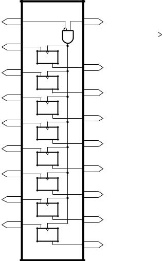
The 74LS377 shown in Fig. 2.17 consists of eight D flip flops all clocked by the same single Clock input C, which is gated by input G. Thus the 8-bit data 8D…1D is clocked in on the / of C if G is Low. In the ANSI/ISO logic diagram shown in Fig. 2.17(b), this dependency is indicated as G1→1C2→2D, which states that G enables the Clock input, which in turn acts on the Data inputs.
Arrays of D flip flops are known as registers; that is read/write memories that hold a single word. The 74LS377 is technically known as a parallel-in parallel-out (PIPO) register, as data is entered in parallel (that is all in one go) and is available to read at one go. D latch arrays are also available, such as the 74LS373 octal PIPO register shown in Fig. 2.18, in which the eight D flip flops are replaced by D latches. In addition the
32 The Quintessential PIC Microcontroller
+5V |
2CLR |
|
2D |
|
2CK |
2SET |
|
2Q |
|
2Q |
|||||||||||||||
|
|
|
|
|
|
|
|
|
|
|
|
|
|
|
|
|
|
|
|
|
|
|
|
|
|
|
|
14 |
|
|
|
13 |
|
|
12 |
|
|
11 |
|
|
10 |
|
|
9 |
|
|
8 |
|
|||
|
|
|
|
|
|
|
|
|
|
|
|
|
|
|
|
|
|
|
|
|
|
||||
|
|
|
|
|
|
|
|
|
|
|
|
|
|
|
1D S Q |
|
|
|
|
|
|||||
|
|
|
|
|
|
|
|
|
|
|
|
|
|
|
|
C1 |
|
|
|
|
|
|
|
|
|
|
|
|
|
|
|
|
|
|
C Q |
|
|
|
|
|
Q |
|
|
|
|
|
|||||
|
|
|
|
|
|
|
|
|
|
|
|
|
|
C |
|
|
|
|
|
||||||
|
|
|
|
|
|
|
|
C1 |
|
|
|
|
|
|
|
|
|
|
|
|
|
|
|
||
|
|
|
|
|
|
|
|
|
|
|
|
|
|
|
|
|
|
|
|
|
|
|
|||
|
|
|
|
|
|
|
1D S Q |
|
|
|
|
|
|
|
|
|
|
|
|
|
|
|
|||
|
|
1 |
|
|
|
2 |
|
|
3 |
|
|
4 |
|
|
5 |
|
|
6 |
|
|
7 |
|
|||
|
|
|
|
|
|
|
|
|
|
|
|
|
|
|
|
||||||||||
|
|
|
|
|
|
|
|
|
|
|
|
|
|
|
|
|
|
|
|
|
|
|
|
|
|
|
|
|
|
|
|
|
|
|
|
|
|
|
|
|
|
||||||||||
1CLR |
|
1D |
1CK |
1SET |
|
1Q |
|
1Q |
GND |
||||||||||||||||
(a) Logic function
|
[74LS74] |
|
|
4 |
S |
5 |
|
3 |
|||
|
|||
C1 |
|
||
2 |
|
||
1D |
6 |
||
|
1R
10
9
11
12
8
13
(b) ANSI/IEC logic symbol
Fig. 2.16 The 74LS74 dual D flip flop.
latch outputs have a 3-state capability. This is useful if data is to be captured and later put onto a common data bus to be read subsequently as desired by a computer.
A pertinent example of the use of a PIPO register is shown in Fig. 2.19. Here an 8-bit ALU is coupled with an 8-bit PIPO register, accepting as its input the ALU output, and in turn feeding one input word back to the ALU. This register accumulates the outcome of a series of operations, and is sometimes called an Accumulator or Working register. To describe the operation of this circuit, consider the problem of adding two words A and B. The sequence of operations, assuming the ALU is implemented by cascading two 74LS382s might be:
1.Program step.
•Mode = 000 (Clear).
•Pulsing Execute loads the ALU output (0000 0000) into the register.
•Data out is zero (0000 0000).
2.Program step.
•Fetch Word A down to the ALU input.
•Mode = 011 (Add).
• Pulse / \ Execute to load the ALU output (Word A + zero) into the register.
•Data out is Word A.
3.Program step.
•Fetch Word B down to the ALU input.
•Mode = 011 (Add).
• / \ Execute to load the ALU output (Word B + Word A) into the register.
2. Logic Circuitry 33
G |
1 |
|
1D |
3 |
|
|
1D |
C1 |
2D |
4 |
|
|
1D |
C1 |
3D |
7 |
|
|
1D |
C1 |
4D |
8 |
|
|
1D |
C1 |
5D |
13 |
|
|
1D |
C1 |
6D |
14 |
|
|
1D |
C1 |
7D |
17 |
|
|
1D |
C1 |
8D |
18 |
|
|
1D |
C1 |
11 C
21Q
52Q
63Q
94Q
12 5Q
156Q
167Q
19 8Q
|
[74LS377] |
|
|||
1 |
G1 |
|
|||
11 |
|
||||
1C2 |
|
||||
18 |
19 |
||||
|
|
|
|||
|
|
|
|||
2D |
|||||
17 |
16 |
||||
|
|
|
|||
|
|
|
|||
|
|
|
|
|
|
14 |
|
|
|
15 |
|
|
|
|
|||
|
|
|
|
|
|
13 |
|
|
|
12 |
|
|
|
|
|||
|
|
|
|
|
|
8 |
|
|
|
9 |
|
|
|
|
|||
|
|
|
|
|
|
7 |
|
|
|
6 |
|
|
|
|
|||
|
|
|
|
|
|
4 |
|
|
|
5 |
|
|
|
|
|||
|
|
|
|
|
|
3 |
|
|
|
2 |
|
|
|
|
|||
|
|
|
|
|
|
|
|
|
|
|
|
(a) Logic function |
(b) ANSI/IEC logic symbol |
Fig. 2.17 The 74LS377 octal D flip flop array.
• Data out is Word B plus Word A.
The sequence of operation codes, that is 000 – 100 – 100 constitutes the program. In practice each instruction would also contain the address (where relevant) in memory of the data to be processed; in this case the locations of Word A and Word B.
Each outcome of a process will have associated properties. For example it may be zero or have a carry-out. Such properties may be significant in the future progress of the program. In the diagram three D flip flops, clocked by Execute, are used to grab this status information. In this situation the flip flops are usually known as flags (or sometimes semaphores). Thus we have Z (Zero), C (Carry from bit 7) and DC (BCD Carry from bit 3) flags, which form a Code Condition or Status register.
34 The Quintessential PIC Microcontroller
LE |
11 |
1 |
OE |
1D |
3 |
C1 1D |
|
|
|
|
|
2D |
4 |
2 |
1Q |
C1 1D |
|
||
|
|
|
|
3D |
7 |
5 |
2Q |
C1 1D |
|
||
|
|
|
|
4D |
8 |
6 |
3Q |
C1 1D |
|
||
|
|
|
|
5D |
13 |
9 |
4Q |
C1 1D |
|
||
|
|
|
|
6D |
14 |
12 |
5Q |
C1 1D |
|
||
|
|
|
|
7D |
17 |
15 |
6Q |
C1 1D |
|
||
|
|
|
|
8D |
18 |
16 |
7Q |
C1 1D |
|
||
|
|
|
|
|
|
19 |
8Q |
|
[74LS377] |
|
|||
1 |
EN |
|
|||
11 |
|
||||
C1 |
|
||||
18 |
19 |
||||
|
|
|
|||
|
|
|
|||
1D |
|||||
17 |
16 |
||||
|
|
|
|||
|
|
|
|||
|
|
|
|
|
|
14 |
|
|
|
15 |
|
|
|
|
|||
|
|
|
|
|
|
13 |
|
|
|
12 |
|
|
|
|
|||
|
|
|
|
|
|
8 |
|
|
|
9 |
|
|
|
|
|||
|
|
|
|
|
|
7 |
|
|
|
6 |
|
|
|
|
|||
|
|
|
|
|
|
4 |
|
|
|
5 |
|
|
|
|
|||
|
|
|
|
|
|
3 |
|
|
|
2 |
|
|
|
|
|||
|
|
|
|
|
|
|
|
|
|
|
|
(a) Logic function |
(b) ANSI/IEC logic symbol |
Fig. 2.18 The 74LS373 octal D latch array.
There are various other forms of register. The 4-bit shift register of Fig. 2.20(a) is an example of a serial-in serial-out (SISO) structure. In this instance the data held in the nth D flip flop is presented to the input of the (n+1)th stage. On receipt of a clock pulse (or shift pulse in this context), this data moves into this (n + 1)th flip flop, i.e. e ectively moving from stage n to stage n + 1. As all flip flops are clocked simultaneously, the entire word moves once right on each shift pulse.
In the example of Fig. 2.20 a 4-bit external data nybble is fed into the left-most stage bit by bit as synchronised by the clock. After four shift pulses the serial 4-bit word is held in the register. To get it out again, four further shifts moves the wrod bit by bit out of the shift register, this is SISO. If the individual flip flops are accessible then the data can be accessed at one go, that is serial-in parallel-out.
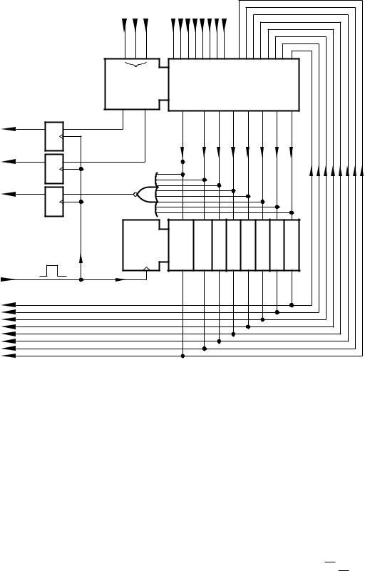
2. Logic Circuitry 35
|
|
Mode |
|
Data in |
|
|
|
|
|
|
|
|||||
|
|
|
0 3 |
P7 |
P5 |
|
P2 |
P0 |
Q7 |
Q5 |
|
Q2 |
Q0 |
|||
|
|
|
P3 |
|
Q3 |
|
||||||||||
|
|
[ALU] |
M- |
P6 P4 |
|
P1 |
Q6 |
Q4 |
|
Q1 |
||||||
|
|
C4 |
C8 |
|
S7 |
|
S6 |
|
S5 |
S4 |
S3 |
|
S2 |
|
S1 |
S0 |
|
DC |
1D |
|
|
|
|
|
|
|
|
|
|
|
|
|
|
|
|
|
|
|
|
|
|
|
|
|
|
|
|
|
|
|
|
|
C1 |
|
|
|
|
|
|
|
|
|
|
|
|
|
|
Status |
C |
1D |
|
|
|
|
|
|
|
|
|
|
|
|
|
|
|
|
|
|
|
|
|
|
|
|
|
|
|
|
|
||
|
C1 |
|
|
|
|
|
|
|
|
|
|
|
|
|
|
|
|
|
|
|
|
|
|
|
|
|
|
|
|
|
|
|
|
|
Z |
1D |
|
|
|
|
|
|
|
|
|
|
|
|
|
|
|
|
|
|
|
|
|
|
|
|
|
|
|
|
|
|
|
|
|
C1 |
|
|
|
|
|
|
|
|
|
|
|
|
|
|
|
|
Working register |
C1 |
|
1D |
|
|
|
|
|
|
|
|
|
|
|
Execute |
|
|
|
|
|
|
|
|
|
|
|
|
|
|
|
|
Data out |
|
|
|
|
|
|
|
|
|
|
|
|
|
|
|
|
Fig. 2.19 An 8-bit ALU-accumulator processor.
The logic diagram of Fig. 2.20(b) uses the → symbol a ected by the clock input to indicate the shift action, C1 →. SRG4 indicates a Shift ReGister 4-stage architecture. An example of an 8-stage shift register is given in Fig. 12.2 on page 307.
Other architectures include parallel-in serial-out which is useful for parallel to serial conversion. Counting registers (counters) increment or decrement on each clock pulse, according to a binary sequence. Typically an n-bit counter can perform a count of 2n states. Some can also be loaded in parallel and thus act as a store.
Consider the negative-edge triggered D flip flop shown in Fig. 2.21 where its Q output is connected back to the 1D input. On each \ at the Clock input C1 the data at the 1D input will be latched in to appear at the Q output. As it is the complement of this output that is fed back to the input, then the next time the flip flop is clocked the opposite logic
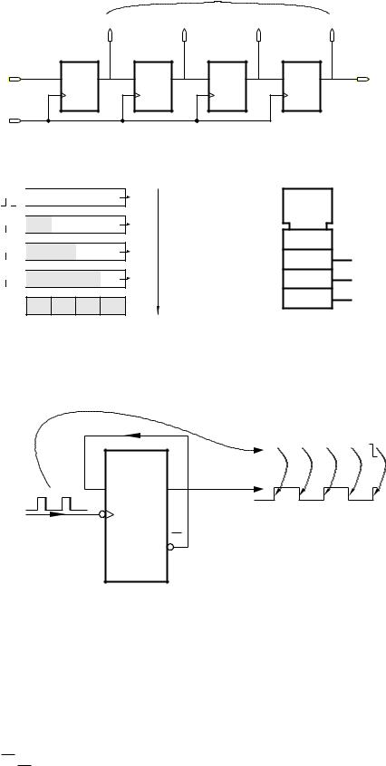
36 The Quintessential PIC Microcontroller
Optional parallel output
Q 0 Q 1 Q 2 Q 3
Serial-in |
1D |
1D |
1D |
1D |
Serial-out |
|
data |
data |
|||||
|
|
|
|
|||
|
C1 |
C1 |
C1 |
C1 |
|
|
Shift |
|
|
|
|
|
|
clock |
|
|
|
|
|
|
(a) A 4-bit shift register |
|
|
|
|
||
(1011) |
0 |
0 |
0 |
0 |
|
|
|
|
|
(101) 1
1  0
0  0
0  0
0  0
0
(10) 1
1  1
1  0
0  0
0  0
0
(1) 0
0  1
1  1
1  0
0  0
0
 0
0  1
1  1
1  0
0
1 0 1 1
(b) Shifting 1011 into the register
Time
SRG4
Shift clock  C1
C1
Serial-in data |
|
1D |
|
Q0 |
|
|
Q1
Q2
Serial-out data/Q3
(c) The ANSII/IEC logic symbol for a SIPO register
Fig. 2.20 The SISO shift register.
|
a |
b |
c |
d |
|
e |
|||||
|
|
|
|
|
|
|
|
|
|
|
|
|
|
|
|
|
|
|
|
|
|
|
|
T T T T T
|
Q |
a b |
1D |
Output a b c d e
C1
Input
Q
Fig. 2.21 The T flip flop.
state will be latched in. This constant alternation is called toggling and is depicted on the diagram by T. The output waveform resulting from a constant frequency input pulse train is half this frequency. This waveform is a precision squarewave, provided that the input frequency remains constant. This T flip flop is sometimes known as a binary or a divide-by-2.
T flip flops can of course be cascaded, as shown in Fig. 2.22(a). Here four \ triggered flip flops are chained, with the output of binary n
2. Logic Circuitry 37
|
1D |
1D |
1D |
1D |
Count |
C1 |
C1 |
C1 |
C1 |
|
|
|
|
|
|
|
|
Q A |
|
|
|
|
|
Q B |
|
Q C |
|
|
|
|
|
Q D |
|
|
|
|
||||||||||||||||
|
|
|
|
|
|
2 |
|
|
|
|
|
|
|
|
4 |
|
|
|
|
|
|
|
|
8 |
|
|
|
|
|
|
|
|
16 |
|
|
|
|
|
|
|
|
|
|
|
|
|
|
|
|
|
|
|
|
|
|
|
|
|
|
|
|
|
|
|
|
|
|
|
|
|
|
|
|||||
(a) Cascading toggle flip flops |
|
|
|
|
|
|
|
|
|
|
|
|
|
|
|
|
|
|
|
|
|
|
|
|
||||||||||||||
Count |
|
|
|
|
|
|
|
|
|
|
|
|
|
|
|
|
|
|
|
|
|
|
|
|
|
|
|
|
|
|
|
|
|
|
|
|
|
|
|
|
|
|
|
|
|
|
|
|
|
|
|
|
|
|
|
|
|
|
|
|
|
|
|
|
|
|
|
|
|
|
|
|
|
|
|
|
|
Q A |
|
|
|
|
|
|
|
|
|
|
|
|
|
|
|
|
|
|
||||||||||||||||||||
0 |
1 |
|
0 |
1 |
0 |
1 |
|
0 |
1 |
0 |
1 |
|
0 |
1 |
0 |
1 |
|
0 |
1 |
0 |
||||||||||||||||||
Q B |
|
|
|
|
|
|
|
|
|
|
|
|
|
|
|
|
|
|
|
|
|
|
||||||||||||||||
0 |
0 |
|
1 1 |
0 |
0 |
|
1 1 |
0 |
0 |
|
1 1 |
0 |
|
0 |
1 |
1 |
0 |
|||||||||||||||||||||
Q C |
|
|
|
|
|
|
|
|
|
|
|
|
|
|
|
|
|
|
|
|
||||||||||||||||||
0 |
0 |
|
0 |
0 |
1 1 1 1 |
0 |
0 |
|
0 |
0 |
1 |
1 |
|
1 |
1 |
0 |
||||||||||||||||||||||
Q D |
|
|
|
|
|
|
|
|
|
|
|
|
|
|
|
|
|
|
|
|||||||||||||||||||
0 |
0 |
|
0 |
0 |
0 |
0 |
|
0 0 |
1 1 |
|
1 1 |
1 |
1 |
|
1 |
1 |
0 |
|||||||||||||||||||||
|
|
|
|
|
|
|
|
|
|
|
|
|
|
|
|
|
|
|
|
|
|
|
|
|
|
|
|
|
|
|
|
|
|
|
|
|
|
|
(b) Resulting |
waveforms |
|
|
|
|
|
|
|
|
|
|
|
|
|
|
|
|
|
|
|
|
|
|
|
|
|
|
|
|
|
||||||||
Fig. 2.22 A modulo-16 ripple counter.
clocking binary n+1. Thus if the input Count frequency was 8 KHz, then QA would be a 4 kHz square waveform and similarily QB would measure in at 2 kHz, QC at 1 kHz, QD at 500 Hz.
The waveform QA of Fig. 2.22(b) was derived in the same manner as in
Fig. 2.21. QB is toggled on each |
|
|
|
of QA and likewise for the |
subsequent |
||
\ |
|
||||||
|
|
4 |
(16) |
||||
outputs. Marking a high as logic 1 and a low as logic 0 gives the 2 |
|
||||||
positive-logic binary patterns as time advances, with the count rolling over back to state 0 on a continual basis. Each pattern remains in the register until the next event clocks the chain; an event being defined in our example as a \ at Count. Examining the sequence shows it to be a natural 8-4-2-1 binary up count, incrementing from 0000b to 1111b. In fact the circuit is a modulo-16 binary counter. A modulo-n count is the sequence taking only the first n numbers into account.8
8Mathematically any number can be converted to its modulo-n equivalent by dividing by n. The remainder, or modulus, will be a number from 0 to n − 1.
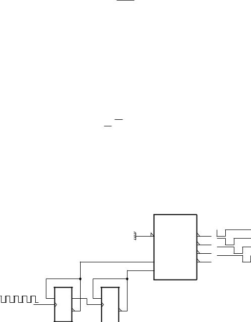
38 The Quintessential PIC Microcontroller
In theory there is no limit to the number of stages that can be cascaded. Thus using eight T flip flops would give a modulo-256 (28) counter. In practice there is a small propagation delay through each stage and this limits the ultimate frequency. For example the 74LS74 dual D flip flop of Fig. 2.16 has a maximum propagation from an event at its Clock input to output of 25 ns. The maximum toggling frequency for a single stage, such as in Fig. 2.21, is given as 25 MHz. An 8-stage counter thus has a maximum ripple-through time of 200 ns. If such a ripple counter were clocked at the resulting 5 MHz (2001ns ) then no sooner than one particular code pattern has stabilized then the next one would begin to appear. This is only really a problem if the various states of the counter are to be decoded and used to control other logic. The decoding logic, such as shown in Fig. 2.23, may inadvertently respond to these short transient states and cause havoc. In such cases more sophisticated synchronous counter configurations are more applicable where the flip flops are clocked simultaneously and steered by the appropriate logic configuration to count in the desired sequence.
The circuit illustrated here implements an up count. If the complement Q lines are used as the outputs, but with the clocking arrangements remaining the same, then the count sequence will decrement, that is a down count. Likewise using / triggered flip flops, such as the 74LS74 dual flip flop (see Fig. 2.23), are used as the storage element, then the count will be down. It is easily possible to use some simple logic to combine the two functions to produce a programmable up/down counter. It is also feasible to provide logic to load the flip flop array in parallel with any number and then count up or down from that point. Such an arrangement can be thought of as a parallel-in counting register.
|
|
|
X/Y |
|
|
|
|
|
[1/2 x 74LS139] |
|
|
|
|
|
EN |
0 |
Ph_1 |
|
|
|
|
||
|
|
|
|
1 |
Ph_2 |
|
|
|
|
2 |
Ph_3 |
|
|
|
1 |
3 |
Ph_4 |
|
|
|
0 |
|
|
|
A |
B |
2 to 4-line |
decoder |
|
|
|
|
|
||
|
1D |
1D |
|
|
|
Clock |
C1 |
C1 |
|
|
|
|
|
|
|
|
|
[74LS74] |
|
Modulo-4 counter |
Fig. 2.23 Generating timing waveforms.

2. Logic Circuitry 39
As well as the more obvious use of a counter register to totalize the number of events, such as cans of peas coming along a conveyor belt, there are other uses. One of these is to time a sequence of operations. In Fig. 2.23 a modulo-4 counter is used to address one section of a 74LS139 2 to 4-line decoder, see Fig. 2.5(a). This detects each of the four states of the counter, and the outcome is four time-separated outputs that can be used to sequence, say, the operation of a computer’s control section logic. As a practical point, the complement Q flip flop outputs have been used to address the decoder to compensate for the / triggered action that would normally give a down count. Larger counters with the appropriate decoding circuitry can be used to generate fairly sophisticated sequences of control operations.
The term register is commonly applied to a read/write memory that can store a single binary word, typically 4 – 64 bits. Larger memories can be constructed by grouping n such registers and selecting one of n. Such a structure is sometimes known as a register file. For example, the 74LS670 is a 4 × 4 register file with a separate 4-bit data input and data output and separate 2-bit address. This means that any register can be read at any time, independently of any concurrent writing process.
|
1 |
|
28 |
|
VDD |
||||
|
|
|
|
|
|
|
|
|
|
A12 |
2 |
27 |
|
R/W |
|||||
|
|
|
|
|
|
|
|
|
|
A7 |
3 |
|
26 |
|
CE2 |
||||
|
|
|
|
|
|
|
|
|
|
A6 |
4 |
|
25 |
|
A8 |
||||
|
|
|
|
|
|
|
|
|
|
A5 |
5 |
|
24 |
|
A9 |
||||
|
|
|
|
|
|
|
|
|
|
A4 |
6 |
|
23 |
|
A11 |
||||
|
|
|
|
|
|
|
|
|
|
A3 |
7 |
22 |
|
OE |
|
|
|||
|
|
|
|
|
|
|
|
|
|
A2 |
8 |
|
21 |
|
A10 |
||||
|
|
|
|
|
|
|
|
|
|
A1 |
9 |
20 |
|
CE1 |
|||||
|
|
|
|
|
|
|
|
|
|
A0 |
10 |
|
19 |
|
I/O7 |
||||
|
|
|
|
|
|
|
|
|
|
I/O0 |
11 |
18 |
|
I/O6 |
|||||
|
|
|
|
|
|
|
|
|
|
I/O1 |
12 |
17 |
|
I/O5 |
|||||
|
|
|
|
|
|
|
|
|
|
I/O2 |
13 |
16 |
|
I/O4 |
|||||
|
|
|
|
|
|
|
|
|
|
VSS |
14 |
|
15 |
|
I/O3 |
||||
(a) Dual in-line package
|
|
RAM |
8192x8 |
|
|
A0 |
0 |
[6264] |
|
I/O7 |
|
|
|
2A |
|||
A1 |
|
|
|
||
|
|
|
1AD |
|
|
A2 |
|
|
|
|
|
|
|
|
2A |
I/O6 |
|
A3 |
|
|
|
||
|
|
|
1AD |
|
|
A4 |
|
|
|
|
|
|
|
|
2A |
I/O5 |
|
A5 |
|
|
|
||
|
|
0 |
1AD |
|
|
A6 |
|
A |
I/O4 |
||
A7 |
|
8191 |
2A |
||
|
|
|
1AD |
|
|
A8 |
|
|
|
|
|
|
|
|
2A |
I/O3 |
|
A9 |
|
|
|
||
|
|
|
1AD |
|
|
A10 |
|
|
|
|
|
|
|
|
2A |
I/O2 |
|
A11 |
|
|
|
||
|
|
|
1AD |
|
|
A12 |
12 |
|
|
|
|
|
|
|
|
||
|
|
|
2A |
I/O1 |
CS2 |
& |
|
1AD |
|
CS1 |
[WRITE] EN1 |
2A |
I/O0 |
|
|
|
1AD |
|
|
|
& |
|
|
|
|
|
|
|
|
OE |
[READ] |
EN2 |
|
|
R/W |
|
|
|
|
(b) Logic symbol
Fig. 2.24 The 6264 8196 × 8 RAM.

40 The Quintessential PIC Microcontroller
Larger read/write memories are normally known as read-write RandomAccess Memories, or RAMs for short. The term random-access indicates that any memory word may be selected with the same access time, irrespective of its position in the memory matrix.9 This contrasts with a magnetic tape memory, where the reel must be wound to the sector in question – and if this is at the end of the tape!
For our example, Fig. 2.24 shows the 6264 RAM. This has a matrix of 65,536 (216) bistables organized as an array of 8192 (213) words of 8 bits. Word n is accessed by placing the binary pattern of n on the 13-bit Address pins A12…A0.
When in the Read mode (Read/Write = 1), word n will appear at the eight data outputs (I/O7…I/O0) as determined by the state n of the address bits. The A symbol at the input/outputs (as was the case in Fig. 2.11) indicates this addressibility. In order to enable the 3-state output bu ers, the Output Enable input must be Low.
The addressed word is written into if R/W is Low. The data to be written into word n is applied by the outside controller to the eight I/O pins. This bi-directional tra c is a feature of computer buses.
In both cases, the RAM chip as a whole is enabled when CS1 is Low and CS2 is High. Depending on the version of the 6264, this access from enabling takes around 100 – 150 ns. There is no upper limit to how long the data can be held, provided power is maintained. For this reason, the 6264 is described as static (SRAM). Rather than using a transistor pair bistable to implement each bit of storage, data can be stored as charge on the gate-source capacitance of a single field-e ect transistor. Such charge leaks away in a few milliseconds, so needs refreshed on a regular basis. Dynamic RAMs (DRAMs) are cheaper to fabricate than SRAM equivalents and obtainable in larger capacities. They are usually found where very large memories are to be implemented, such as found in a personal computer. In such situations, the expense of refresh circuitry is more than amortized by the reduction in cost of the memory devices.
Both types of Read/Write memories are volatile, that is they do not retain their contents if power is removed. Some SRAMs can support existing data at a very low holding current and lower than normal power supply voltage. Thus a backup battery can be used in such circumstances to keep the contents intact for many months.
9Strictly speaking, ROMs should also be described as random access, but custom and practice has reserved the term for read-write memories.