


137
6
Electron Microscopy Techniques for Characterization of Nanomaterials
Jian-Min (Jim) Zuo
This chapter describes the practice and theory of electron imaging and diffraction for structural analysis of nanomaterials. It is demonstrated that the information obtainable from electron diffraction with a small probe and strong interactions complements other characterization techniques, such as x-ray and neutron diffraction that samples a large volume and real-space imaging by HREM with a limited resolution. The recent developments in electron energy filtering, 2-D digital detectors and computer-based image analysis and simulations have significantly improved the quantification of electron diffraction. Examples are given to demonstrate the resolution and sensitivity of electron diffraction to individual nanostructures.
6.1
Introduction
This chapter describes electron microscopy techniques for nanomaterials characterization. The focus is on nanocrystallography for the study of the atomic and molecular structure of structural forms that have the feature of being from a few to hundreds of nanometers in length. The microscopy techniques have the potential to provide quantitative structural data for individual nanostructures in a role similar to x- ray and neutron diffraction for bulk crystals. This potential is currently being developed for the reasons that electron diffraction patterns can be recorded selectively from individual nanostructures at sizes as small as a nanometer using electron probe-forming lenses and apertures, while electron imaging provides direct realspace structural information.
The chapter is organized in seven sections. Sections 6.2 and 6.3 form an introduction to electron diffraction techniques and theory, while Section 6.4 introduces highresolution electron imaging. Section 6.5 focuses on experimental data analysis. The emphasis is on recently developed coherent nanoarea electron diffraction and electron diffraction from individual nanostructures. Section 6.6 gives two examples of nanostructure characterization using a combination of electron imaging and diffraction.
At the center of electron nanocrystallography is high-resolution electron diffraction and imaging. While high-resolution electron microscopy (HREM) performed at
Nanofabrication Towards Biomedical Applications. C. S. S. R. Kumar, J. Hormes, C. Leuschner (Eds.) Copyright 2005 WILEY-VCH Verlag GmbH & Co. KGaA, Weinheim
ISBN 3-527-31115-7

138 6 Electron Microscopy Techniques for Characterization of Nanomaterials
magnifications of > 100K and resolution that is capable of resolving crystal lattices has become one of the major techniques since its development in the early 1980s, the development of high-resolution electron diffraction, at the convergence of several microscopy technologies, is relatively new. The development of field emission guns (FEG) in the 1970s and their adoption in conventional transmission electron microscopes (TEM) brought high source brightness, small probe size, and coherence to electron diffraction. The significant impact is the ability to record diffraction patterns to obtain crystallographic information from very small (nano) structures. The electron energy filter, such as the in-column energy filter with four magnets that bend the electron beam into an X shape (X-filter), allows inelastic background from plasmon and higher electron energy losses to be removed with an energy resolution of a few electron volts. The development of array detectors of charge-coupled device (CCD) cameras or imaging plates enables parallel recording of diffraction patterns and quantification of diffraction intensities over a large dynamic range that was not available to electron microscopy before. The post specimen lenses of the TEM give the flexibility of recording electron diffraction patterns at different magnifications. Last, but just as important, the development of efficient and accurate algorithms to simulate electron diffraction and modeling structures on a first-principle basis using fast modern computers has significantly improved our ability to interpret experimental diffraction patterns.
For readers new to electron microscopy, there are a number of introductory books [1–4]. Kinematical approximation for electron diffraction and the diffraction geometry for qualitative analysis of electron diffraction patterns are covered in Ref. [1]. The book by Williams and Carter is an excellent introductory textbook for students [3]. More specialized books on electron imaging and diffraction can be found in Refs. [5–8].
6.2
Electron Diffraction and Geometry
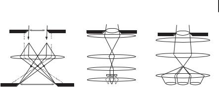
Electron optics in a microscope can be configured for different diffraction modes, from parallel-beam illumination to convergent beams. Figure 6.1 illustrates three modes of electron diffraction: selected area electron diffraction (SAED), nanoarea electron diffraction (NED) and convergent-beam electron diffraction (CBED). Variations from these three techniques include large-angle CBED [9], convergent-beam imaging [10], electron nanodiffraction [11], and their modifications [12]. For nanostructure characterization, the electron nanodiffraction technique developed by Cowley [11] and others in the late 1970s using a scanning TEM (STEM) is particularly relevant. In this technique, a small electron probe of a size from a few angstroms to a few nanometers is placed directly onto the sample. A diffraction pattern can thus be obtained from a localized area as small as a single atomic column, which is very sensitive to local structure and probe positions. Readers interested in these techniques can find their description and applications in above references.
|
|
6.2 |
Electron Diffraction and Geometry 139 |
|
a |
b |
c |
|
Virtual |
|
|
|
Aperture |
|
|
Specimen |
|
C2 Aperture |
|
|
P’ |
Condenser II |
|
|
10µm |
|
|
|
P |
Condenser Lens III |
Upper |
|
|
|
|
|
|
|
Objective |
Lower Objective |
|
Upper Objective |
|
Back Focal Plan |
|
Specimen |
|
Lens |
|
||
|
|
|
|
|
|
Lower Objective |
Lower |
|
|
Specimen |
|
|
|
|
Objective |
|
SA Aperture |
Back Focal Plane |
Back Focal Plan |
|
|
||
Selected-Area Electron Diffraction |
Nanoarea Electron Diffraction |
Convergent-Beam Electron Diffraction |
|
Figure 6.1. Three modes of electron diffraction. Both (a) selected area electron diffraction (SAED) and (b) nanoarea electron diffraction (NED) use parallel illumination. SAED limits the sample volume contributing to electron diffraction by using an aperture in the image
6.2.1
Selected-Area Electron Diffraction
plane of the image-forming lens (objective). NED achieves a very small probe by imaging the condenser aperture on the sample using a third condenser lens. Convergent-beam electron diffraction (CBED) uses a focused probe.
SAED is formed by placing an aperture in the imaging plane of the objective lens [see Fig. 6.1(a)]. Only rays passing through this aperture contribute to the diffraction pattern at the far field. For a perfect lens without aberration, these rays come from an area defined by the back-projected aperture image. The aperture image is typically a factor of 20 smaller because of the demagnification of the objective lens. In a conventional electron microscope, the difference in the focus for rays at different angles to the optic axis due to the objective lens aberration results a displaced aperture image for each diffracted beams. Take the rays marked P and P¢ for an example. While ray P being parallel to the optical axis defines the ideal back-projected aperture image, ray P¢ at an angle of a will move by aberration a distance y=Csa3. For a microscope with Cs=1 mm and a=50 mrad, this gives a displacement of 125 nm. The smallest area that can be selected in SAED is thus limited by the objective lens aberration.
The combination of imaging and diffraction in SAED mode makes it particularly useful for setting diffraction conditions for electron imaging in a TEM, such as lattice images or diffraction contrast. It is also one of the major electron microscopy techniques for materials phase identification and orientation determination. The interpretation of SAED for materials phase identification, orientation relationships, and defects is described by Edington [1].
6.2.2
Nano-Area Electron Diffraction
Figure 6.1(b) shows a schematic diagram of the principle of parallel-beam electron diffraction from a nanometer-sized area in a TEM. The electron beam is focused to
140 6 Electron Microscopy Techniques for Characterization of Nanomaterials
the focal plane of the objective prefield, which then forms a parallel-beam illumination on the sample. For a condenser aperture of 10 mm in diameter, the probe diameter is ~50 nm, which is much smaller than the smallest area that can be achieved in conventional SAED, and does not suffer from aberration-induced image shift (see above). The diffraction pattern recorded in this mode is similar to that in SAED, e.g., the diffraction pattern consists of sharp diffraction spots for perfect crystals.
NED in a FEG microscope also provides higher beam intensity than SAED (the probe current intensity is ~105 e s–1 nm–2), since all electrons illuminating the sample are recorded in the diffraction pattern. The small probe size enables us to select an individual nanostructure for electron diffraction.
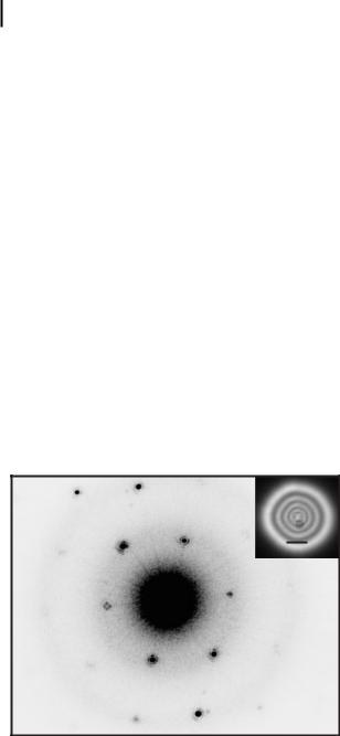
The application of nanoarea electron diffraction for electron nanocrystallography is demonstrated in Fig. 6.2, which shows an experimental diffraction pattern recorded from a single Au nanocrystal close to the [110] zone axis. The small illumination enables the isolation of a single nanocrystal for diffraction. The parallel beam gives the high angular resolution for the recording of details of diffuse scattering that comes from finite size and deviations from a ideal crystal structure.
The NED technique described here is different from electron nanodiffraction in a STEM [9]. In electron nanodiffraction, the beam is focused on, or near, the sample. A small condenser aperture is used to reduce the beam convergence angle. The beam convergence limits the angular resolution in recorded diffraction patterns. Many nanostructures are nonperiodic and lack the perfect crystal order resulted from either the small size or atomic arrangements. Their diffraction patterns are diffuse as shown in Fig. 6.2. High angular resolution is thus required for recording diffuse scattering.
10 nm
[110]
Figure 6.2. An example of nanoarea electron diffraction. The diffraction pattern was recorded from a single Au nanocrystal of ~4 nm near the zone axis of [110]. Around each diffraction spot, two rings of oscillation are clearly
visible. The rings are not continuous because of the shape of the crystal. The electron probe and an image of the nanocrystal are shown top right.
6.2 Electron Diffraction and Geometry 141
A third condenser lens, or a minilens, provides the flexibility and demagnification for the formation of a nanometer-sized parallel beam. In the design of electron microscopes with a two condenser lenses illumination system, the first lens is used to demagnify the electron source and the second lens transfers the demagnified source image to the sample at focus (for probe formation) or underfocused to illuminate a large area. The condenser aperture is placed after the second lens.
6.2.3
Convergent-Beam Electron Diffraction
CBED is formed by focusing the electron probe at the specimen [see Fig. 1(c)]. Compared to SAED, CBED has two main advantages for studying perfect crystals or the local structure of polycrystalline materials or crystals with defects:
1.The pattern is taken from a much smaller area with a focused probe; The smallest electron probe currently available in a high-resolution FEG-STEM is close to 1 &. Thus, in principle and in practice, CBED can be recorded from individual atomic columns. For crystallographic applications, CBED patterns are typically recorded with a probe of a few to tens of nanometers.
2.CBED patterns record diffraction intensities as a function of incident-beam directions. Such information is very useful for symmetry determination and quantitative analysis of electron diffraction patterns.
b*
a*
P’ 
 P
P
a |
b |
Figure 6.3. A comparison between CBED and SAED. (a) Recorded diffraction pattern along [001] from magnetite cooled to liquid nitrogen temperature. There are two types of diffraction spots, strong and weak ones. The weak ones come from the low-temperature structural
transformation. All diffraction spots in this pattern can be indexed based on two reciprocal lattice vectors (a* and b*). (b) Recorded CBED pattern from spinel MgAl2O4 along [100] at 120 kV.

142 6 Electron Microscopy Techniques for Characterization of Nanomaterials
A comparison between SAED and CBED is given in Fig. 6.3. CBED patterns consist of disks. Each disk can be divided into many pixels, and each pixel approximately represents one incident beam direction. For an example, let us take the beam P in Fig. 6.3. This particular beam gives one set of diffraction pattern shown as the full lines. The diffraction pattern by the incident beam P is the same as the selected area diffraction pattern with a single parallel incident beam. For a second beam P¢, which comes at different angle compared to P, the diffraction pattern in this case is displaced from that of P by a/k with a as the angle between the two incident beams.
Experimentally, the size of the CBED disk is determined by the condenser aperture and the focal length of the probe-forming lenses. In modern microscopes with an additional minilens placed in the objective prefield, it is also possible to vary the convergence angle by changing the strength of the minilens. Underfocusing the electron beam also gives a smaller convergence angle, but it leads to a bigger probe, which can be an issue for specimens with a large wedge angle.
The advantage of being able to record diffraction intensities over a range of incident beam angles makes CBED readily accessible for comparison with simulations. Because of this, CBED is a quantitative diffraction technique. In the past 15 years, CBED has evolved from a tool primarily for crystal symmetry analysis to the most accurate technique for structure refinement and strain and structure factor measurement [13]. For defects, large-angle CBED technique can characterize individual dislocations, stacking faults, and interfaces. For applications to defect structures and structure without three-dimensional periodicity, parallel-beam illumination with a very small beam convergence is required.
6.3
Theory of Electron Diffraction
Electron diffraction from a nanostructure can be alternatively described by electrons interacting with an assembly of atoms (ions) or from a crystal of finite size and shape. Which description is more appropriate depends on which is a better approximation of the structure. Both cases are covered here. We start with kinematical electron diffraction from a single atom, then move on to the assembly of atoms and to crystals. Electron multiple scattering, or electron dynamic diffraction, is strong in perfect crystals, but can be neglected to the first-order approximation for very small nanostructures or macromolecules such as carbon nanotubes made of mostly light atoms.
6.3.1
Kinematic Electron Diffraction and Electron Atomic Scattering
Electron interacts with an atom by the Coulomb potential of the positive nucleus and the electrons surrounding the nucleus. The relationship between the potential and the atomic charge is given by the Poisson equation:

|
|
~ ~ |
6.3 Theory of Electron Diffraction |
143 |
r |
2 V ~r |
e½ZdðrÞ rðrÞ& |
(1) |
|
|
||||
ð Þ ¼ |
eo |
|
|
Here V is the potential, the electron density, e the electron charge, eo the vacuum permitivity, and Z the atomic number. If we take a small volume, d~r ¼ dxdydz, of the atomic potential at position ~r, the exit electron wave ue from this small volume is approximately given by:
ue » ð1 þ ipkUdxdydzÞuo |
(2) |
~ |
2 |
Here we take U ¼ 2meVðrÞ=h , where m is relativistic mass of high-energy elec- |
|
trons and h is the Planck constant. k is the electron wavelength. The interaction potential U is treated as constant within the small volume. Equation (2) is known as parallel beam of incident electrons, the
the weak-phase-object approximation. For a |
|
|
|
|
|
|
|
|
|
|
|
|||||||||||||||||||||
|
|
|
|
|
|
|
|
|
|
|
|
|
|
|
|
|
|
|
|
|
|
|
|
|
|
~ ~ |
|
|
|
|
|
|
incident wave is described by the plane wave exp 2piko r . For high-energy elec- |
||||||||||||||||||||||||||||||||
trons with E>>V, the scattering by the atom is weak and we have approximately: |
||||||||||||||||||||||||||||||||
|
|
|
2pme |
Ð |
|
|
~ |
|
~ ~ |
|
~ |
~ |
|
|
|
|
|
|
|
|
|
|
|
|
|
|
||||||
u |
¼ |
|
|
VðrÞ |
e2pikjr rj e2piko |
r¢ d~r¢ |
|
|
|
|
|
|
|
|
|
|
|
|
(3) |
|||||||||||||
|
|
|
2 |
|
|
|
|
|
|
|
|
|
|
|
|
|
|
|||||||||||||||
s |
|
|
h |
|
|
|
~r |
|
~r |
|
|
|
|
|
|
|
|
|
|
|
|
|
|
|
|
|
|
|
||||
|
|
|
|
|
|
|
|
|
j ¢j |
|
|
|
|
|
|
|
|
|
|
|
|
|
|
|
|
|
|
|
||||
|
|
|
|
|
|
|
|
|
|
|
|
|
|
|
|
|
|
|
~ |
|
~ |
|
|
|
|
|
~ |
|
~ |
|
~ |
|
Far away from the atom, we have jrj >> jr¢j. By replacing jr |
r |
¢j |
with jrj in the |
|||||||||||||||||||||||||||||
denominator and |
|
|
|
|
|
|
|
|
|
|
|
|
|
|
|
|
|
|
|
|
|
|
||||||||||
|
|
|
|
|
|
|
|
|
~ ~ |
|
|
|
|
|
|
|
|
|
|
|
|
|
|
|
|
|
|
|
|
|||
~r |
|
~r¢ |
j |
» r |
|
r¢ r |
|
|
|
|
|
|
|
|
|
|
|
|
|
|
|
|
|
|
|
|
(4) |
|||||
j |
|
|
|
|
|
r |
|
|
|
|
|
|
|
|
|
|
|
|
|
|
|
|
|
|
|
|
|
|
||||
for the exponential, we obtain |
|
|
|
|
|
|
|
|
|
|
|
|
|
|
|
|
||||||||||||||||
|
|
|
|
|
|
|
|
|
|
|
|
|
|
|
|
|
~ |
|
|
|
|
|
|
~ ~ |
|
|
2pi |
~k ~k |
|
~r¢ |
||
|
|
|
2pme |
Ð |
|
V |
~r¢ |
|
|
2pik ~r ~r¢ |
|
|
|
2pme e |
2piko r Ð |
|
|
|||||||||||||||
|
|
|
|
|
|
|
|
2piko ~r¢ |
|
|
|
|
|
|
|
o |
|
|
||||||||||||||
u |
¼ |
|
|
|
|
|
|
|
~r |
ð |
Þ |
e |
j |
j e |
|
|
d~r¢ » |
|
|
|
|
|
|
V ~r¢ |
e ð |
|
|
Þ |
d~r¢ |
|||
|
|
|
|
|
|
|
|
|
|
|
|
r |
|
|
||||||||||||||||||
s |
|
|
h |
2 |
|
|
|
|
~r |
|
|
|
|
|
|
h |
2 |
|
|
ð Þ |
|
|
|
|
|
(5) |
||||||
|
|
|
|
|
|
|
|
|
j ¢j |
|
|
|
|
|
|
|
|
|
|
|
|
|
|
|
|
|
||||||
~ |
|
|
|
Here k is the scattered wave vector and the direction is taken along ~r. The half of |
|||
~ |
~ |
~ |
|
¼ k |
ko =2, is |
||
the difference between the scattered wave and incident wave, s |
|||
defined as the scattering vector. As we will see later, this vector is half the reciprocal lattice vector (g) for the Bragg diffraction of a crystal. From Eq. (5), we define electron atomic scattering factor
|
2pme Ð |
~ |
4pi~s ~r¢ ~ |
|
|
f ðsÞ ¼ |
h2 |
|
Vðr¢Þe |
dr¢ |
(6) |
The potential is related to the charge density; Fourier transform of electron charge density is commonly known as the x-ray scattering factor. It can be shown that the relationship between the electron and x-ray scattering factors is given by
f |
|
s |
|
|
me2 |
|
ðZ f x Þ |
¼ |
0:023934 |
ðZ f x Þ |
(&) |
(7) |
||||||
|
Þ ¼ 8peo h2 |
|||||||||||||||||
|
ð |
|
|
s2 |
|
|
|
|
s2 |
|
|
|||||||
The x-ray scattering factor in the same unit is given by |
|
|||||||||||||||||
|
|
|
|
|
|
|
! |
|
|
|
|
|
|
|
|
|
|
|
f |
x |
ðsÞ ¼ |
|
e2 |
|
f |
x |
¼ 2:82 · 10 |
5 |
f |
x |
(&) |
|
(8) |
||||
|
|
mc2 |
|
|
|
|
|
|||||||||||
144 |
6 Electron Microscopy Techniques for Characterization of Nanomaterials |
|
|
|
|
|
|
|
|
For typical value of s~0.2 &–1, the ratio f = e2 =mc2 |
f x ~104. Thus electrons are scat- |
tered by an atom much more strongly than x-ray. There are two consequences as the result of this: one is that electrons are much more sensitive to a small volume of materials, such as nanostructures, and the other is multiple scattering. For a thick crystal, electron multiple scattering is a serious effect, while multiple scattering is generally weak in most x-ray structural analyses.
The electron distribution in an atom depends on the atomic electronic structure and bonding with neighboring atoms. At sufficiently large scattering angles, we can approximate the atoms in a crystal by spherical free atoms or ions. Atomic charge density and the Fourier transform of the charge density can be calculated with high accuracy. The results of these calculations are published in the literature and tabulated in the international table for crystallography. Tables optimized for electron diffraction applications are also available [14].
6.3.2
Kinematical Electron Diffraction from an Assembly of Atoms
Here, we extend our treatment of kinematical electron scattering from a single atom to an assembly of atoms. For nanostructures of a few nanometers, the treatment outlined here forms the basis for electron diffraction pattern analysis and interpretation. For a large assembly of atoms in a crystal with well-defined 3-D periodicity, we use this section to introduce the concepts of lattice and reciprocal space, which are the foundation for the treatment of crystal diffraction.
Kinematic scattering from an assembly of atoms follows the same treatment as for a single atom:
|
|
|
|
|
|
~ ~ |
|
|
2pi ~k ~k ~r¢ |
|
|
|
|
|
~ ~ |
|
|
|
|
|
|
|
|
|
2pme |
|
e |
2piko r Ð |
|
|
|
2pme e |
2piko r |
|
|
|
|
||||||
u |
|
» |
|
|
|
V ~r¢ |
e |
ð o Þ |
d~r¢ |
¼ |
|
FT |
ð |
V ~r¢ |
ÞÞ |
(9) |
|||||
|
h2 |
|
|
r |
|
h2 |
|
|
|
||||||||||||
|
s |
|
ð Þ |
|
|
|
r |
ð |
|
||||||||||||
Here FT denotes Fourier transform. The potential of an assembly of atoms can be
expressed as a sum of potentials from individual atoms |
|
|||||
|
|
|
|
|
|
|
P P |
|
~ |
~ |
|
||
~ |
|
Vi |
(10) |
|||
VðrÞ ¼ |
j |
|
r |
rj |
||
i |
|
|
|
|
|
|
The summations over i and j are for the type of atoms and atoms of each type respectively.
To see how an atomic assembly diffracts differently from a single atom, we first look at a row of atoms that are separated periodically by an equal spacing of a. Each atom contributes to the potential at point ~r. The total potential is obtained by summing up the potential of each atom. If we take the x-direction along the row, then
|
* |
|
N |
|
|
|
|
P |
^ |
|
|
V |
¼ |
~ |
(11) |
||
r |
VA ðr |
naxÞ |
n¼1
The sum can be considered as placing an atom on each of a collection of points; these points describe the geometrical arrangement of the atoms. In a crystal, the pe-
6.3 Theory of Electron Diffraction 145
riodic arrangement of points defines the lattice. In both cases, the potential of an assembly of atoms is a convolution of the atomic potential and the lattice:
|
|
|
N |
|
|
V |
* |
~ |
P ~ |
^ |
(12) |
r |
¼ VA ðrÞ |
dðr |
naxÞ |
n¼1
The Fourier transform of this potential [see Eq. (9)] is the product of Fourier trans-
form of the atomic potential and Fourier transform of the lattice: |
|
|||
|
" N |
|
# |
|
|
P |
dðr naxÞ |
(13) |
|
FT½VðrÞ& ¼ FT½VA ðrÞ& FT |
||||
~ |
~ |
~ |
^ |
|
n¼1
The Fourier transform of atomic potential gives the atomic scattering factor. The
Fourier transform of an array of delta functions gives |
|
|
|
|
|
|
||||||||||
|
|
|
|
|
|
|
|
|
h |
|
|
|
|
i |
|
|
|
" N |
|
|
# |
N |
~ ~ |
|
|
|
~ ~ |
~xNa |
|
||||
|
P |
|
|
|
P |
|
sin p k |
k |
|
|
||||||
FT |
d ~r |
|
nax^ |
Þ |
¼ |
e 2piðk ko Þ ~xna |
¼ |
|
h |
|
|
o |
|
i |
(14) |
|
|
|
|
|
|
|
|
|
|||||||||
|
ð |
|
|
|
sin |
~ ~ |
~ |
|
|
|||||||
|
n¼1 |
|
|
|
n¼1 |
|
|
|
p k ko |
xa |
|
|||||
The function of Eq. (14) has an infinite number of maxima at the condition:
|
|
|
|
|
~ |
~ |
^ |
¼ h=a |
(15) |
k |
ko |
x |
Here h is an integer from –1 to 1. The maxima are progressively more pronounced with increasing N. For sufficiently large N, Eq. (14) reduces to a periodic array of delta functions with the spacing of 1/a.
For a three-dimension periodic array of atoms, where the position of atoms is given by the integer displacement of the unit cell a, b, and c, the potential is given by
|
|
|
|
|
|
|
|
|
P |
|
|
|
|
~ |
|
|
|
|
|
||||||
* |
|
¼ VA |
|
* |
|
|
|
|
~ |
~ |
|
~ |
|
|
|
|
(16) |
||||||||
V r |
|
|
r |
|
|
|
|
|
|
|
|
|
|
|
|||||||||||
|
|
|
d r |
na |
mb lc |
|
|
|
|
||||||||||||||||
|
|
|
|
|
|
|
|
|
|
|
|
n;m;l |
|
|
|
|
|
|
|
|
|
|
|
|
|
The Fourier transform of the three-dimensional lattice of a cube N0N0N gives |
|
||||||||||||||||||||||||
" |
N |
|
N |
|
|
N |
|
|
|
|
|
* |
|
# |
|
|
|
|
|
|
|||||
P P P |
~ |
~ |
|
|
~ |
|
|
|
|
|
|
|
|
|
|||||||||||
FT |
|
|
|
|
|
|
|
|
mb |
|
¼ |
|
|
|
|
|
|
||||||||
¼ |
1 m |
¼ |
1 l |
¼ |
d r |
na |
lc |
|
|
|
|
|
|
||||||||||||
h |
1 |
|
|
|
|
|
|
|
|
|
|
|
|
|
|
|
|
|
|||||||
n |
|
|
|
|
|
|
|
|
|
|
|
|
|
|
|
|
|
|
|
||||||
|
|
|
|
|
i h |
|
i h |
i |
|
||||||||||||||||
sin h |
|
~ ~ |
|
|
|
|
|
~ ~ |
|
~ |
|
|
|
|
~ ~ |
i |
(17) |
||||||||
|
|
|
|
o |
i |
h |
|
o |
i |
|
|
|
h |
|
o |
||||||||||
p |
k |
|
k |
|
|
~aN sin p |
k |
k |
|
bN |
|
|
sin p |
k k |
~cN |
|
|||||||||
sin |
|
~ ~ |
|
~ |
|
|
|
~ ~ |
~ |
|
|
sin p |
~ ~ |
~ |
|
|
|||||||||
p k ko a |
|
|
|
sin p k ko |
b |
|
|
|
k ko |
c |
|
||||||||||||||
Similar to the one-dimensional case, Eq. (17) defines an array of peaks. The position of the peaks is placed where
|
~ |
|
~ |
a ¼ h |
|
k |
ko |
|
|
|
~ |
~ |
~ |
~ |
¼ k |
(18) |
k |
ko |
b |
||
~ |
~ |
c ¼ l |
|
|
k |
ko |
|
||
|
|
~ |
|
|

146 6 Electron Microscopy Techniques for Characterization of Nanomaterials
with h, k, and l as integers. It can be shown that
* |
* |
* |
~ |
|
|
~ |
|
~ |
|
|
|
|
(19) |
||
|
|
|
|
|
|
|
|
|
|
|
|
||||
Dk ¼ k k o ¼ ha |
þkb |
þlc |
|
|
|
|
|||||||||
and |
|
|
|
|
|
|
|
|
|
|
|
||||
|
|
|
~ |
|
|
|
|
~c |
~a |
|
|
|
|
~ |
|
|
|
|
b ·~c |
|
|
|
|
|
|
~a · b |
|
||||
~a |
|
|
|
|
, ~b |
|
ð · |
Þ |
,~c |
|
|
|
|
(20) |
|
|
|
|
|
|
|
|
|
|
|||||||
¼ |
~ |
~ |
~ |
¼ |
~ |
~ |
~ |
¼ |
~ |
~ |
~ |
|
|||
|
a |
b |
· c |
|
|
a |
b |
· c |
|
a |
b |
· c |
|
||
The vectors a*, b*, and c* together define the three-dimensional reciprocal lattice. For nanostructures that have the topology of a periodic lattice, we can be describe
the structure by the lattice plus a lattice-dependent displacement: |
|
|||||||||
|
|
P |
|
|
|
|
|
|
|
|
* |
* |
~ |
~ |
~ ~ |
~ |
~ |
~ |
~ |
(21) |
|
V r |
¼ VA r |
|||||||||
d r |
R |
uðRÞ |
, with R |
¼ na |
mb |
lc |
||||
n;m;l
For simplicity, we will restrict the treatment to monoatomic primitive lattices. Generalization to complex cases with nonprimitive lattices follows the same principle and will lead to similar qualitative conclusions, but more complex expressions.
The Fourier transform of the lattice gives a sum of two terms: |
|
|
|||||||||||
" P |
|
~ |
|
|
# |
P |
|
~ |
h |
i |
|
||
FT |
|
~ |
|
~ ~ |
¼ |
|
~ |
|
~ ~ ~ |
(22) |
|||
|
d r |
R |
uðRÞ |
exp 2piDk |
R exp 2piDk u R |
||||||||
|
n;m;l |
|
|
|
|
|
n;m;l |
|
|
|
|
|
|
For small displacement, Eq. (22) can be expanded to the first order |
|
||||||||||||
" P |
|
~ |
|
|
# |
|
|
|
|
|
|
|
|
FT |
|
~ |
|
~ ~ |
|
|
|
|
|
|
|
||
n;m;l |
d r |
R |
uðRÞ ¼ |
|
|
|
|
|
|
||||
|
|
|
|
|
|
|
|
|
|
|
|
|
|
|
|
|
|
|
|
|
|
|
|
|
|
||
P |
|
|
~ |
~ |
|
P |
~ |
~ ~ |
|
~ |
~ |
|
|
|
exp |
|
|
|
|
|
(23) |
||||||
|
2piDk |
R |
|
þ 2piDk |
u R |
exp 2piDk |
R |
|
|||||
n;m;l |
|
|
|
|
|
n;m;l |
|
|
|
|
|
|
|
The first term is the same as Eq. (17), which defines an array of diffraction peaks; the position of each peak is defined by the reciprocal lattice of the averaged crystal structure. Compared to infinite crystals, the diffraction peak of a finite crystal has a broad distribution, which is defined by the shape of the crystal. The second term describes the diffuse scattering around a reflection defined by the crystal reciprocal lattice. If we take the reflection as g and write
~ |
~ |
~ |
~ |
~ |
¼ 2np |
|
|
|
|
|
|
|
(24) |
Dk |
¼ g |
þ q and g |
R |
|
|
|
|
|
|
|
|||
For |g|>>|q|, the diffuse scattering term can be rewritten as |
|
|
|||||||||||
|
|
|
|
|
|
|
|
|
|
|
|
|
|
P |
|
~ |
~ ~ |
|
~ |
~ |
» |
P |
~ ~ ~ |
~ |
~ |
|
|
|
|
exp |
|
(25) |
|||||||||
|
2piDk |
u R |
2piDk |
R |
|
2pig u R |
exp |
2piq |
R |
||||
n;m;l |
n;m;l |
6.4 High-Resolution Electron Microscopy 147
Equation (25) is the Fourier sum of the displacements along the g direction. The intensity predicted by this equation will increase with a g2-dependence. The atomic scattering contains the Debye–Waller factor, which describes the damping of highangle scattering because of thermal vibrations. The balance of these two terms results in a maximum contribution to the diffuse scattering from the structural deviation from the ideal crystal lattice [5].
The oscillations from the finite size of the nanocrystals are clearly visible in the diffraction pattern shown in Fig. 6.2. The subtle differences in the intensity oscillations for different reflections can come from several factors, including surface relaxation, the small tilt and curvature of the Ewald sphere, and nonnegligible multiple scattering effects for heavy atoms such as Au. The surface relaxation can be treated using the approximation described above.
In summary, we have described a kinematical theory for an atomic assembly by considering the interplay between ordering among atoms, the finite sizes, and the structural modification. Qualitatively, we expect to find several features in the diffraction pattern of an assembly of atoms, including intensity maxima from ordering of atoms, diffuse scattering from the outline shape of the atomic assembly, and structural modification in the form of atomic displacements. The characteristics of diffuse scattering from the shape and atomic displacements are different. While the shape function is same for all reflections, diffuse scattering from atomic displacement has a characteristic distribution. This difference can be used in experimental studies to distinguish these two effects [5].
6.4
High-Resolution Electron Microscopy
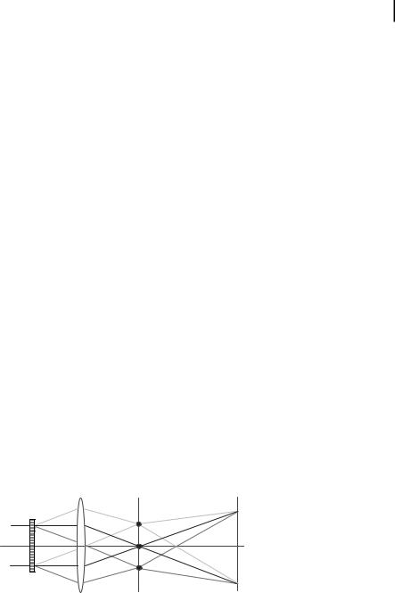
Transmission high-resolution electron images are formed by recombining diffracted beams of the back focal plane of the image formation (objective) lens at the imaging plane (see Fig. 6.4). While electron diffraction records structural information in the reciprocal space, electron imaging gives direct information about local structure and morphology with near-atomic resolution. Information from HREM is complemen-
Object
Lens |
Back Focal Plane Image Plane |
|
(diffraction) |
Figure 6.4. High-resolution electron image formation, where the diffraction pattern is formed at the back focal plane of the objective lens and diffracted beams recombine to form image.

148 6 Electron Microscopy Techniques for Characterization of Nanomaterials
tary to electron diffraction. However, interpretation of HREM images requires the knowledge of image formation and the contrast transfer function of the electron image formation lens.
For very small nanostructures or weakly scattering objects, the object potential is weak. Under such condition, following Eq. (2), the exit electron wave function is approximately given by
|
|
(26) |
ue ðx; y; zÞ » 1 þ ipkUðx; yÞ |
||
Here |
|
|
|
Ðt |
|
|
(27) |
|
Uðx; yÞ ¼ Uðx; y; zÞdz |
||
|
0 |
|
is the projected potential along the electron beam direction. The potential U(x,y,z) is measured in ngstrom–2 (see the relationship between U and V in Section 3.1). U is electron acceleration voltage dependent because of relativistic effects. Equation (27) is often called the weak phase approximation. For U~5010–2 &–2, electron wavelength k~0.02 &, Eq. (27) is a reasonable approximation for thickness t < 100 &.
The contrast of electron image depends on focus and the objective lens aberrations. Among many forms of aberrations, the spherical aberration Cs and chromatic aberration Cc are the dominant ones for a conventional TEM. To look at the effect of these two aberrations, the aperture and defocus on imaging, let us start with a sinusoidal weak phase object such that
ue ðx; yÞ » 1 þ iecosð2pqxÞ |
(28) |
The Fourier transform of this wave function is three delta functions:
|
|
|
|
|
|
ue kx ; ky |
»d kx ; ky |
þ ie d kx q; ky |
þ d kx þ q; ky |
=2 |
(29) |
For the purpose of discussion now, we omit the aperture function. In this case, the wave function at the back focal plane is given by
|
|
|
|
|
|
|
|
|
|
|
|
||
uf kx ; ky |
» d kx ; ky |
þ ie d kx q; ky |
þ d kx þ q; ky |
=2 |
exp iv kx ; ky |
(30) |
|||||||
Here |
|
|
|
|
|
|
|
|
|
|
|
|
|
|
|
h |
2 |
2 i"Cs k2 h 2 |
2 i |
|
# |
|
|
(31) |
|||
v kx ; ky |
|
¼ |
kx |
þ ky |
|
|
kx |
þ ky |
þ Df |
|
|
||
|
2 |
|
|
|
|||||||||
is the phase shift introduced by the spherical aberration (Cs) of the image formation lens and defocus (Df). The electron image is a Fourier transform of Eq. (30)
ui ðxÞ ¼ 1 ecosð2pqxÞsin vðqÞ þ iecosð2pqxÞsin vðqÞ |
(32) |

6.4 |
High-Resolution Electron Microscopy |
149 |
From this we obtain the image intensity |
|
|
|
|
|
IðxÞ ¼ 1 ecosð2pqxÞsin vðqÞ 2 þ e2 cos2 ð2pqxÞsin2 vðqÞ |
||
¼ 1 2ecosð2pqxÞsin vðqÞ þ e2 cos2 ð2pqxÞ |
(33) |
|
. 1 2ecosð2pqxÞsin vðqÞ |
|
|
The approximation is for small e under the weak phase object assumption. Equation (33) shows that in addition to the amplitude of the original wave, the
image intensity modulation also depends on the sine function of the aberrated phase. The difference between the maximum and minimum intensities gives the image contrast. The maximum contrast is obtained by having sin vðqÞ ¼ 1 or
vðqÞ ¼ p=2, in which case, IMax IMin ¼ 4e. The contrast transfer function is the ratio of the difference with sin vðqÞ „ 1and 4e, defined by:
CTF |
¼ |
IMax IMin |
¼ |
j4esin vðqÞj |
¼ j |
sin v q |
Þj |
(34) |
|
IMax IMin MAX |
|||||||||
|
4e |
ð |
|
Thus, the objective lens’s imaging properties are described by the contrast transfer function (CTF). Since CTF is independent of the object, it provides a convenient mechanism for understanding the imaging process and contrast. For an object with many frequencies, CTF gives the relative contribution of each frequency to the final image in coherent imaging.
The maximum contrast is obtained when the phase shift is p/2 and the optimum is that this is achieved for as many frequencies as possible. The condition for this, known as the Scherzer focus, is obtained under the following conditions for aperture angle a and defocus Df :
!1=4
aopt ¼ 1:41 |
k |
; Dfopt ¼ ðCs kÞ |
1=2 |
(35) |
Cs |
|
At Scherzer focus the half-width of the image intensity of a point object is given
by
|
3 |
1=4 |
dh ¼ 0:43 Cs k |
|
(36) |
This is often used as a measurement of the electron microscope resolution. For Cs=0.5 mm, k=0.025 &, d=1.28 &.
The focal length of electron lenses depends on electron energy. Chromatic aberration comes from the finite electron energy spread, objective lens current fluctuations, and high voltage instability. All of these introduce an envelope function to the contrast transfer function
h q |
2 i |
|
KC ¼ exp |
|
(37) |
K |
||

150 6 Electron Microscopy Techniques for Characterization of Nanomaterials
Here, K is a function of the chromatic aberration coefficient, the energy spread, lens current, and high voltage fluctuations.
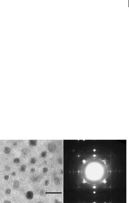
Figure 6.5 shows a high-resolution image of gold nanoparticles recorded at the Scherzer focus condition. The image was recorded using the Lawrence Berkeley Laboratory One-&ngstrom Microscope [15]. The basic instrument is a modified Philips CM300FEG/UT, a TEM with a field-emission electron source and an ultra-twin objective lens with low spherical aberration (Cs = 0.65 mm) and a native resolution of 1.7 &. The size of the particles ranges from 2 to ~3 nm. The particles were supported on a thin carbon film.
Figure 6.5. High-resolution image of 2~3 nm gold nanoparticles under the Scherzer focus condition. The direct, atomic-reso- lution image clearly reveals the diversity of structures, from sin- gle-crystal to twinned particles.
Another high-resolution electron imaging technique is scanning transmission electron microscopy (STEM). In STEM, electrons are focused into a very small probe and scanned across the sample. Electrons scattered by the sample are detected to form an image. The image intensity is approximately proportional to the square of atomic number, Z2, if only electrons scattered into high angles are detected using a high-angle annual dark-field (HAADF) detector [16].

6.5 Experimental Analysis 151
6.5
Experimental Analysis
6.5.1
Experimental Diffraction Pattern Recording
The optimum setup for quantitative electron diffraction is the combination of a flexible illumination system, an imaging filter, and an array of 2-D detectors with a large dynamic range. The three diffraction modes described in Section 6.2 can be achieved through a three-lens condenser system. Currently both the JEOL (JEOL, USA) and Zeiss microscopes offer this capability. Two types of energy filter are currently employed: one is the in-column X-energy filter [17] and the other is the postcolumn Gatan imaging filter (GIF) [18]. Each has its own advantages. The in-col- umn X-filter takes the full advantage of the postspecimens lens of the electron microscope and can be used in combination with detectors such as film or imaging plates (IP), in addition to the CCD camera. For electron diffraction, geometric distortion, isochromaticity, and angular acceptance are the important characteristics of filters [19]. Geometrical distortion complicates the comparison between experiment and theory and is best corrected by experiment. Isochromaticity defines the range of electron energies for each detector position. Ideally this should be the same across the whole detector area. Angular acceptance defines the maximum range of diffraction angles that can be recorded on the detector without a significant loss of isochromaticity.
Current 2-D electron detectors include CCD cameras and imaging plates (IP). The performance of the CCD camera and IP for electron recording has been measured [20]. Both are linear with large dynamic range. At low dose range, the CCD camera is limited by the readout noise and dark current of CCD. The readout noise places a limit on what information can be recovered from recorded images if the CCD camera has a limited resolution. IP has a better performance at low dose range due to the low dark current and readout noise of the photomultiplier. For medium and high dose, the IP is limited by linear noise due to the granular variation in the phosphor and instability in the readout system. The CCD camera is limited by the linear noise in the gain image, which can be made very small using averaging. There is an uncertainty in the uniformity of CCD because of its dependence on the gain image as prepared in the electron microscope. The performance of CCD also varies from one camera to another, which makes the individual characterization necessary.
The noise in the experimental data can be estimated using the measured detector quantum efficiency (DQE) of the detector
varðIÞ ¼ mgI=DQEðIÞ |
(38) |
Here I is the estimated experimental intensity, var denotes the variance, m is the mixing factor defined by the point spread function, and g is the gain of the detector [20]. This expression allows an estimation of variance in experimental intensity once DQE is known, which is especially useful in the v2 -fitting, where the variance is used as the weight.

1526 Electron Microscopy Techniques for Characterization of Nanomaterials
6.5.2
The Phase Problem and Inversion
In the kinematic approximation, the diffracted wave is proportional to the Fourier transform of the potential [Eq. (9)]. If both the amplitude and phase of the wave are known, then an image can be reconstructed, which would be proportional to the projected object potential. In recording a diffraction pattern, however, what is recorded is the amplitude square of the diffracted wave. The phase is lost. The missing phase is known as the phase problem. In the case of kinematic diffraction, the missing phase prevents reconstruction of the object potential by inverse Fourier synthesis. The phase is preserved in imaging up to the information limit. In electron imaging, the scattered waves recombine to form an image by the transformation of a lens and the intensity of the image is recorded, not the diffraction. The complication in imaging is the lens aberration. Spherical aberration introduces an additional phase to the scattered wave. This phase oscillates rapidly as the scattering angle increases. Additionally, chromatic aberration and the finite energy spread of the electron source impose a damping envelope to the CTF [Section 6.4] and limit the
highest-resolution information (information limit) that passes through the lens. As result, the phase of scattered waves with sin h=k > 1 &–1 is typically lost in electron images and the resolution of image is ~1 & for the best microscopes currently available. Phase retrieval is a subject of great interest in both electron and x-ray diffraction. If the phase of a diffraction pattern can be found, then an image can be formed without a lens.
In electron diffraction, the missing phase has not been a major obstacle to its application. The reason is electron imaging and that, for most electron diffraction applications, electrons are multiply scattered. The missing phase is the phase of the exit wave function. Inversion of exit wave function to object potential is not as straightforward as an inverse Fourier transform. A theory developed by two research groups (Spence at Arizona State University and Allen in Australia) shows the principle of inversion using data sets of multiple thicknesses, orientations, and overlapping coherent electron diffraction [21]. The inversion is based on the scattering matrix that relates the scattered wave to the incident wave. This matrix can be derived based on the Bloch wave method, which has a diagonal term of exponentials of the product of eigenvalues and thickness. Electron diffraction intensities determine the moduli of all elements of the scattering matrix. Using the properties of scattering matrix (unitarity and symmetries), an overdetermined set of nonlinear equations can be obtained from these data. Solution of these equations yields the required phase information and allows the determination of a (projected) crystal potential by inversion [22].
For materials’ structural characterization, in many cases, the structure of materials is approximately known. What is to be determined is the accurate atomic positions and unit cell sizes. Extraction of these parameters can be done in a more efficient manner using the refinement technique [23]. Another important fact is that the phase of object potential is actually contained in the diffraction pattern through electron interference when electrons are elastically scattered for multiple times [24].

6.5 Experimental Analysis 153
For nanostructures such as carbon nanotubes laid horizontally, the number of atoms is low along the incident electron beam direction. Electron diffraction, to a good approximation, can be treated kinematically. Many nanostructures also have a complicated structure. Modeling, as required in the refinement technique, is difficult because of the lack of knowledge about the structure. The missing phase then becomes an important issue. Fortunately, the missing phase is actually easier to retrieve for nonperiodic objects than for periodic crystals. The principle and technique for phase retrieval are described next.
6.5.3
Electron Diffraction Oversampling and Phase Retrieval for Nanomaterials
Electron phase retrieval uses a coherent electron probe. The formation of a coherent electron probe in NED mode follows the same principle as STEM probe formation, but in a reverse optical geometry. In STEM, a parallel coherent illumination is brought into focus by the electron objective lens. The phase difference from lens aberration, defocus, and convergence angle defines the size and shape of the electron probe. In NED mode, a focused probe (by the condenser lens) at the front focal plane of the preobjective lens is imaged into a nearly parallel beam. Because of the lens aberration, beams at different angles to the optic axis are imaged at different distances.
For small nanostructures, such as carbon nanotubes, electron diffraction is well described by the kinematical approximation. At a small scattering angle, the scattered electron wave is a sum of the scattered waves over the volume of the structure:
|
|
Ð |
~~ |
|
~ ~ |
|
|
Ð |
~~ |
|
~ ~ |
~ |
» |
~ |
2pik r¢ |
uo |
~ |
þ ipk |
~ |
2pik r¢ |
uo |
||
us k |
½1 þ ipkUðr¢Þ&e |
|
ðr¢Þdr¢ ¼ uo |
k |
Uðr¢Þe |
|
ðr¢Þdr¢ |
(39)
~
Here Uð~rÞ is the interaction potential defined in Section 3.1 and k is the scattered wave vector. The illuminating electron wave function uoð~rÞ is formed by the electron lens as described above. Information about the structure is carried in the second term. For an idealized plane wave illumination, the electron diffraction intensity can
|
|
|
|
|
|
~ |
be expressed through the Fourier transform of the potential UðkÞ as: |
||||||
|
|
|
|
|
|
2 |
~ |
~ |
þ ðpkÞ |
2 |
U |
~ |
|
I k |
» d k |
|
k |
(40) |
||
For a finite nanostructure, the diffraction intensity is continuous in reciprocal space.
Using the combination of coherent NED and phase retrieval, we have demonstrated for the first time that atomic resolution can be achieved from diffraction intensities without an imaging lens [25]. This technique was applied to image the atomic structure of a double-wall carbon nanotube (DWNT). The electron diffraction pattern from a single DWNT was recorded and phased. The resolution is limited by the diffraction intensity. The resolution obtained for the DWNT was 1 & from a microscope of a nominal resolution of 2.3 &.

154 6 Electron Microscopy Techniques for Characterization of Nanomaterials
The principle of phase retrieval for a localized object is based on the sampling theory. For a localized object of size S, the minimum sampling frequency (Nyquist frequency) in reciprocal space is 1/S. Sampling with a smaller frequency (oversampling) increases the field of view. Wavefunctions at these oversampled frequencies are a combination of the wavefunctions sampled at the Nyquist frequency. Because of this, phase information is preserved in oversampled diffraction intensities. Oversampling can be achieved only for a localized object. For a periodic crystal, the smallest sampling frequency is the Nyquist frequency. The iterative phasing procedure works by imposing the amplitude of the diffraction pattern in the reciprocal space and the boundary conditions in real space. The procedure was first developed by Fienup [26] and improved by incorporating other constraints such as symmetry [27]. The approach of diffractive imaging, or imaging from diffraction intensities, appears to solve many technical difficulties in conventional imaging of nonperiodic objects, namely, resolution limit by lens aberration, sample drift, instrument instability, and low contrast in electron images.
The phase retrieval procedure works by starting with the measured amplitude of the Fourier transform and random phases: an estimate of the projected potential is computed and modified to satisfy the real-space constraints. The modified potential is Fourier transformed and the calculated amplitudes are replaced by their measured values. The procedure is repeated until a self-consistent solution of the potential is found. The amplitudes of the Fourier transform of the potential are obtained based on Eq. (40). There are two major constraints that can be used for electron phase retrieval: one is the approximate shape of the object from low-resolution imaging and the other is positivity. Outside the image, we assume a constant project potential, which acts as the support. The projected potential is assumed positive (the same sign).
We use the modified hybrid-input-output (HIO) algorithm outlined by Millane and Stroud [27] for iterative phase retrieval. The working principle of this algorithm is shown in Fig. 6.6. The procedure starts with an estimated image fn and calculate the constrained image cn. The support constrain is applied by using
|
G’n |
|
Inverse Fourier |
|
|
|
|
fn |
||
|
|
|
Transform |
|
|
|
|
|
|
|
|
|
|
|
|
|
|
|
|
|
|
|
|
|
|
|
|
|
|
|
|
|
|
|
|
|
|
|
|
|
|
Calculate real-space |
|
Calculate amplitudes |
|
|
|
|
|
|
|
constrained image Cn |
||
and phases; replace |
|
|
|
|
|
|
|
|
|
|
|
|
|
|
|
|
|
|
Cn |
||
with experimental |
|
|
|
gn |
|
|||||
|
|
|
|
|||||||
amplitudes |
|
|
|
|
|
|||||
|
|
|
Apply Equation 43 |
|||||||
|
|
|
|
|
|
|
|
|
||
|
|
|
|
|
|
|
|
|
||
|
|
|
|
|
|
|
|
|
|
|
|
|
|
|
|
|
|
|
|
|
|
|
|
|
Forward Fourier |
|
|
|
|
|
|
|
|
Gn |
|
Transform |
|
|
|
|
gn+1 |
||
|
|
|
|
|
|
|
|
|||
|
|
|
|
|
|
|
||||
Figure 6.6. The flow chart of hybrid input and output algorithm for iterative phase retrieval. (After Ref. [273].)
|
|
|
6.5 |
Experimental Analysis |
155 |
~ |
~ |
˛ S |
|
(41) |
|
|
|
||||
Cn ðrÞ ¼ 0, r |
|
|
|||
and |
|
|
|
|
|
~ |
|
~ |
˛ O |
(42) |
|
Cn ðrÞ > 0; and real r |
|
||||
where S and O denote regions of support and the object. From the initial image and the calculated constrained image cn, a driver function gn+1 is derived:
g ~r |
|
fn ðrÞ |
|
if jCn ðrÞ fn ðrÞj < e |
(43) |
||||
nþ1 ð Þ ¼ |
|
|
~ |
|
|
~ |
~ |
|
|
g |
~r b C |
~r f |
~r |
if C |
~r f |
~r |
> e |
|
|
|
|
n ð Þ þ ½ |
n ð Þ |
n ð Þ& |
j |
n ð Þ |
n ð Þj |
|
|
When the phase of this driver function is combined with the experimental amplitude data they yield an image fn+1 that more closely satisfies the real-space constraint than the original image fn+1. The alternative is to take
~ |
~ |
(44) |
gnþ1 ðrÞ ¼ Cn ðrÞ |
||
giving the error-reduction (ER) algorithm. It has been found that it is often useful to mix HIO with a few iterations of ER. We found that the ER algorithm is often efficient at the initial stage of iteration, but HIO is always more efficient at late-stage iterations.
Figure 6.7 shows a small DWNT reconstructed from the recorded electron diffraction pattern. The scattering of carbon is generally too weak for direct imaging of the atomic structure in an electron microscope. Diffractive imaging avoids this problem by recording the diffraction pattern, which has a better signal-to-noise ratio than the image because of the highly ordered (helical) structure of carbon nanotubes. Details of the tube structure are clearly visible. The potential profile demonstrates the type of information that can be obtained from the reconstructed image.
0.060
0.055
0.050
0.045
0.040
0.035
0.030
0.025
0.020
0.015
2.91 nm 0.010
a
Figure 6.7. (a) The recorded electron from a single double-wall carbon nanotube, (b) the reconstructed image using HIO algorithm,
(c) the profile of reconstructed potential
0.005
0.000
-0.005
0 |
10 |
20 |
30 |
40 |
50 |
60 |
70 |
80 |
90 |
b c
averaged over the middle section of the image; the profile is consistent with a concentric hollow tube.

1566 Electron Microscopy Techniques for Characterization of Nanomaterials
6.6
Applications
6.6.1
Structure Determination of Individual Single-Wall Carbon Nanotubes
For simple structures, such as single-wall carbon nanotubes (SWNTs), the structure can be determined uniquely from the diffraction pattern alone. Carbon nanotubes have attracted extraordinary attention due to their unique physical properties, from atomic structure to mechanical and electronic properties, since Iijima showed the first high-resolution TEM image and electron diffraction of multiwall carbon nanotubes [28]. A SWNT can be regarded as a single layer of graphite that has been rolled
up into a cylindrical structure. In general, the tube is helical with the chiral vector
|
|
~ |
|
|
~ |
ðn; mÞ defined by c ¼ na þ mb, where c is the circumference of the tube and a and b |
|||||
~ |
~ |
|
~ |
~ |
|
are the unit vectors |
of the |
graphite sheet. |
A striking feature is that tubes with |
||
n m ¼ 3l (l is a integer) are metallic, while others are semiconductive [29]. This unusual property, plus the apparent stability, has made carbon nanotubes an attractive material for constructing nanoscale electronic devices. As-grown SWNTs have a dispersion of chirality and diameters. Hence, a critical issue in carbon nanotube applications is the determination of individual tube structure and its correlation to the properties of the tube. This requires a structural probe that can be applied to individual nanotubes.
Gao et al. have developed a quantitative structure determination technique for SWNTs using NED [30]. This, coupled with improved electron diffraction pattern interpretation, allows determination of both the diameter and the chiral angle, and thus the chiral vector ðn; mÞ, of an individual SWNT. The carbon nanotubes they studied were grown by chemical vapor deposition. TEM observation was carried out in a JEOL2010F TEM with a high voltage of 200 keV.
Figure 6.8 shows the diffraction pattern from a SWNT. The main features of this pattern are: (i) a relatively strong equatorial oscillation which is perpendicular to the tube direction, and (ii) some very weak diffraction lines from the graphite sheet, which are elongated in the direction normal to the tube direction [31]. The intensities of diffraction lines are very weak in this case. In their experimental setup, the strongest intensity of one pixel is about 10 counts, which corresponds to ~12 electrons.
The diameter of the tube is determined from the equatorial oscillation, while the chiral angle is determined by measuring the distances from the diffraction lines to the equatorial line. The details are following. The diffraction of SWNT is well described by kinematic diffraction theory (Section 6.3). The equatorial oscillation in the Fourier transformation of a helical structure like SWNT is a Bessel function with n=0 [32] which gives:
2Ðp |
2 |
I0 ðXÞ / J02 ðXÞ / cosX cosXdX |
(45) |
0
6.6 Applications 157
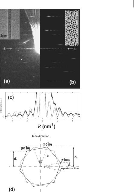
Figure 6.8. (a) A diffraction pattern from an individual SWNT 1.4 nm in diameter. The inset is a TEM image. The radial scattering around the saturated (000) is an artifact from aperture scattering. (b) Simulated diffraction pattern of a (14,6) tube. The inset is the corresponding structure model. (c) Profiles of equatorial
oscillation along EE¢ from (a, b) and simulation for (14,6). (d) Schematic diagram of electron diffraction from an individual SWNT. The two hexagons represent the first order graphite-like {100} diffraction spots from the top and bottom of the tube.

158 6 Electron Microscopy Techniques for Characterization of Nanomaterials
Here X ¼ 2pRr0 ¼ pRD0, R is the reciprocal vector which can be measured from the diffraction pattern, and D0 is the diameter of the SWNT. We use the position of J02ðXÞ maxima (Xn, n ¼0, 1, 2, ...) to determine the tube diameter. With the first several maxima saturated and inaccessible, Xn=Xn 1 can be used to determine the number N for each maximum in the equatorial oscillation. Thus, by comparing the experimental equatorial oscillation with values of Xn, the tube diameter can be uniquely determined.
To measure chirality from the diffraction pattern, Fig. 6.8(d) is considered, which shows the geometry of the SWNT diffraction pattern based on the diffraction of the top-bottom graphite sheets. The distances d1; d2; d3 relate to the chiral angle a by:
d1 þ d2 |
¼ d3 , |
|
|
|
|
|
|
|
|
|
|
|
|
|
|
|
|
|
|
|
|
||||
a |
|
atan |
1 |
|
|
d2 d1 |
|
|
atan |
1 |
|
2d2 d3 , |
(46) |
||||||||||||
¼ |
ðp3 |
|
|
Þ ¼ |
ðp3 |
|
|||||||||||||||||||
|
|
|
|
|
d |
3 |
|
|
|
|
d |
3 |
Þ |
|
|
||||||||||
|
|
|
|
|
|
|
|
|
|
|
|
|
|
|
|
|
|
|
|
|
|
|
|
||
|
|
|
|
|
p |
|
|
d1 |
|
|
|
|
p |
d3 |
d2 |
|
|
||||||||
or b |
¼ |
atan |
ð |
|
3 |
|
d2 þd3 |
Þ ¼ |
atan |
ð |
|
3 |
|
d2 |
þd3 |
Þ |
|
||||||||
|
|
|
|
|
|
|
|
|
|
|
|
|
|
. |
|
||||||||||
These relationships are not affected by the tilting angle of the tube (see below). Because d2 and d3correspond to the diffraction lines having relatively strong intensities and are further from the equatorial line, they are used in our study instead of d1 to reduce the error. The distances can be measured precisely from the digitalized patterns. The errors are estimated to be <1% for the diameter determination and <0.2 for the chiral angle.
Using the above methods, the SWNT giving the diffraction pattern shown in Fig. 6.8 was determined to have a diameter of 1.40 nm (–0.02 nm) and a chiral angle of 16.9 (–0.2 ). Among the possible chiral vectors, the best match is (14,6), which has a diameter of 1.39 nm and a chiral angle of 17.0 . The closest alternative is (15,6), having a diameter eof 1.46 nm and a chiral angle of 16.1 , which is well beyond the experiment error. Figure 6.8(b) plots the simulated diffraction pattern of (14,6) SWNT from the structure model shown in the inset. Figure 6.8(c) compares the equatorial intensities of experiment and simulation. These results show an excellent agreement.
6.6.2
Structure of Supported Small Nanoclusters and Epitaxy
Nanometer-sized structures in the forms of clusters, dots, and wires have recently received considerable attention for their size-dependent transport, optical, and mechanical properties. The focus is on synthesizing nanostructures of desired shapes with narrow size distributions. For clusters or nanocrystals on crystalline substrates, epitaxy gives lower interface energy and can lead to enhanced stability and better control over the interfacial electronic properties. At the nanometer scale, cluster equilibrium shape is also determined by the surface, interface, and strain energies. A challenge, thus, is how to determine the structure of individual clusters. The case highlighted below on Ag on Si (100) is taken from the experimental work by Li et al.
6.6 Applications 159
at University of Illinois, Urbana-Champaign. Over the past three years, they have carried out a systematic study of nanoclusters’ structure and interfaces using a combination of electron diffraction and microscopy [33–36].
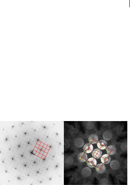
Figure 6.9 shows the electron diffraction patterns for samples deposited on H-ter- minated Si (100) surfaces. The diffraction patterns were taken off the [100] zone axis to avoid strong multiple scattering in zone axis orientation. The diffraction pattern of the as-deposited sample consists of a strong and continuous Ag {111} ring, short Ag {200} arcs on a weak Ag {200} ring, short Ag {220} arcs on a weak Ag {220} ring and weak {311} rings. Upon annealing at 400 C, Ag (020) and (002) reflection intensities increase significantly. Both have diffuse streaks along (011) and (0–11) directions. The Ag (020) and (002) are asymmetrical because of the off-zone axis orientation of the diffraction pattern. Meanwhile, the diffraction intensity in the continuous ring decreases significantly, but remains visible. Figure 6.9 shows high-resolution images of Ag clusters on H-Si(100) after annealing with strong moir fringe contrast. These images were taken at the Si [100] zone axis. At this orientation, the Si (022) and (0–22) planes are imaged. Most as-grown Ag clusters show no visible moir fringes, which is consistent with the diffraction pattern that is dominated by a {111} ring. A few clusters with moir fringes are often defective. In Fig. 9, the clusters of dark contrast with no moir fringes contribute to the {111} ring in the diffraction pattern. For as deposited clusters (not shown here), at first sight, the orientation of these clusters appears to be random. However, a close inspection of the diffraction pattern shows a much weaker {200} ring than what it would be in a powder diffraction pattern of random polycrystalline Ag. For single crystals oriented with Ag(111)//Si(100) or Ag(100)//Si(100), strong Ag {220} is expected in both cases, while a strong Ag {200} is also expected in the case of Ag(111)//Si(100). Both of these cases can be ruled out. In Fig. 6.9, the square Ag clusters with 2-D moir fringes (from interference between Ag and Si lattices [2]) perfectly
Si
Ag
10 NM
Figure 6.9. Combined electron diffraction and imaging characterization of epitaxial Ag nanoclusters/nanocrystals on Si (100) substrate.

160 6 Electron Microscopy Techniques for Characterization of Nanomaterials
parallel to Si (220) lattice planes, in good agreement with the electron diffraction analysis. At this stage, the transformation from random orientation to epitaxial growth is not finished, because we still see weak-contrast Ag clusters, supposed to be random Ag clusters. The Ag {200} reflections have the shape of a plus-sign, centered at the Ag {200} position, suggestive of perfect cubic Ag nanocrystals, with their edges perfectly aligned to the Si (011) and (01–1) directions.
6.7
Conclusions and Future Perspectives
This chapter has described the practice and theory of electron imaging and diffraction for structural analysis of nanomaterials and has demonstrated that the information obtainable from electron diffraction with a small probe and strong interactions complements other characterization techniques, such as x-ray and neutron diffraction that samples a large volume and real-space imaging by HREM with a limited resolution.
The challenge is to extend the applications of microscopy techniques to soft and biomaterials, where radiation-induced structural damage is more likely to occur at high electron dose levels. While radiation tolerance can be significantly improved with cryo-electron microscopy, the ultimate image resolution will be limited by the low signal-to-noise ratio resulting from the low electron dose that the sample can tolerate [4, 37]. The sensitivity demonstrated here for carbon nanotubes would also be useful for imaging molecular structures.
Abbreviations
CBED – convergent-beam electron diffraction
CCD – charge coupled device
CTF – contrast transfer function
DQE – detector quantum efficiency
DWNT – double-wall carbon nanotube
FEG – field emission guns
GIF – Gatan imaging filter
HAADF – high-angle annual dark-field
HIO – hybrid-input-output
HREM – high-resolution electron microscopy
IP – imaging plates
NED – nanoarea electron diffraction
SAED – selected area electron diffraction
STEM – scanning transmission electron microscope
SWNT – singlewall carbon nanotube
TEM – transmission electron microscopes

References 161
Acknowledgments
Work was supported by DOE DEFG02–01ER45923 and DEFG02–91ER45439 and uses the TEM facility of the Center for Microanalysis of Materials at Materials Research Laboratory. The author would like to thank R. Zhang and L. Nagahara (Motorola Labs) for providing the carbon nanotubes, Dr. M. O’Keefe and Chris Nelson for Fig. 6.5, Dr. Min. Gao for Fig. 6.8, and Boquan Li for Fig. 6.9.
References
1J.W. Edington, Practical Electron Microscopy in Materials Science, Monograph 2, Electron Diffraction in the Electron Microscope, MacMillan, Philips Technical Library, 1975.
2P. Hirsch et al., Electron Microscopy of Thin Crystals, R. E. Krieger, Florida, p. 19, 1977.
3D. B. Williams, C. B. Carter, Transmission Electron Microscopy, Plenum, New York, 1996.
4L. Reimer, Transmission Electron Microscopy, 4th edn, Springer, Berlin,1997.
5J. M. Cowley, Diffraction Physics, North-Hol- land, New York, 1981.
6 J. C. H. Spence, J. M. Zuo, Electron Microdiffraction, Plenum, New York, 1992.
7Z. L. Wang, Elastic and Inelastic Scattering in Electron Diffraction and Imaging, Plenum, New York, 1995.
8E. J. Kirkland, Advanced Computing in Electron Microscopy, Plenum Press, New York, 1998.
9M. Tanaka, M. Terauchi, T. Kaneyama,
Convergent-Beam Electron Diffraction, JEOL,
Tokyo, 1988.
10J. P. Morniroli, Electron Diffraction, Dedicated Software to Interpret LACBED Patterns, USTL, Lille, France, 1994.
11J. M. Cowley, Electron nanodiffraction,
Microsc. Res. Tech. 46, 75, 1999.
12L. J. Wu, Y. M. Zhu, J. Tafto, Picometer accuracy in measuring lattice displacements across planar faults by interferometry in coherent electron diffraction, Phys. Rev. Lett. 85, 5126, 2000.
13J. M. Zuo, Quantitative convergent-beam electron diffraction, Materials Trans. JIM 39, 938–946, 1998.
14L. M. Peng, Electron atomic scattering factors and scattering potentials of crystals, Micron 30, 625, 1999.
15M. A. O’Keefe, C. J. D. Hetherington, Y. C. Wang, E. C. Nelson, J. H. Turner,
C. Kisielowski, J. O. Malm, R. Mueller,
J. Ringnalda, M. Pan, A. Thust, Ultramicroscopy, 89, 215, 2001.
16P. D. Nellist, S. J. Pennycook, High angular dark field scanning transmission electron microscopy, in Advances in Imaging and Electron Physics, vol. 113, ed. P. W. Hawkes, Academic Press, San Diego, p. 147, 2000.
17L. Reimer, ed., Energy-Filtering Transmission Electron Microscopy, Springer, Berlin, 1995.
18O. L. Krivanek, S. L. Friedman, A. J. Gubbens,
B.Kraus, An imaging filter for biological applications, Ultramicroscopy, 59, 267, 1995.
19H. Rose, in Energy-Filtering Transmission Electron Microscopy, ed. L. Reimer, Springer, Berlin, 1995.
20J. M. Zuo, Electron detection characteristics of a slow-scan CCD camera, imaging plates and film, and electron image restoration,
Microsc. Res. Tech. 49, 245, 2000.
21J. C. H. Spence, Direct inversion of dynamical electron diffraction patterns to structure factors, Acta Cryst. A54, 7, 1998.
22L. J. Allen, T. W. Josefsson, H. Leeb, Obtaining the crystal potential by inversion from electron scattering intensities, Acta Cryst. A54, 388, 1998.
23J. M. Zuo, Measurements of g electron densities in Solids, Rep. Prog. Phys. 67, 2053, 2004.
24J. M. Zuo, J. C. Spence, R. Hoier, Accurate structure-factor phase determination by elec- tron-diffraction in noncentrosymmetric crystals, Phys. Rev. Lett. 62, 547, 1989.
25J. M. Zuo, I. Vartanyants, M. Gao, R. Zhang,
L.A. Nagahara, Atomic resolution imaging of a single double-wall carbon nanotube from diffraction intensities, Science, 300, 1419–1421, 2003.

162 6 Electron Microscopy Techniques for Characterization of Nanomaterials
26J. Fienup, Phase retrieval algorithms – a comparison, Appl. Opt., 21, 2758, 1982.
27R. P. Millane, W. J. Stroud, Reconstructing symmetric images from their undersampled Fourier intensities, J. Opt. Soc. Am. A. 14, 568, 1997.
28S. Iijima, Helical microtubules of graphitic carbon, Nature 354, 56, 1991.
29J. W. Mintmire, B. I. Dunlap, C. T. White, Are fullerene tubules metallic? Phys. Rev. Lett. 68, 631, 1992.
30M. Gao, J. M. Zuo, R. D. Twesten, I. Petrov, L. A. Nagahara, R. Zhang, Structure determination of individual single-wall carbon nanotubes by nano-area electron diffraction, Appl. Phys. Lett. 82, 2703–2706, 2003.
31S. Amelinckx, A. Lucas, P. Lambin, Electron diffraction and microscopy of nanotubes,
Rep. Prof. Phys. 62, 1471, 1999.
32D. Sherwood, Crystal, X-rays and Proteins.
John Wiley & Sons, New York, 1976.
33B. Q. Li, J. M. Zuo, Self-assembly of epitaxial Ag nanoclusters on H-terminated Si (111) surfaces, J. Appl. Phys. 94, 743–748, 2003.
34J. K. Bording, Y. F. Shi, B. Q. Li, J. M. Zuo, Sizeand shape-dependent energetics of nano-crystal interfaces: experiment and simulation, Phys. Rev. Lett., 90, 226104, 2003.
35B. Q. Li, J. M. Zuo, The development of epitaxy of nanoclusters on lattice-mismatched substrates: Ag on H-Si(111) surfaces, Surf. Sci. 520, 7–17, 2002.
36J. M. Zuo, B. Q. Li, Nanostructure evolution during cluster growth: Ag on H-terminated Si(111) surfaces, Phys. Rev. Lett. 88, 255502,
2002.
37R. Henderson, The potential and limitations of neutrons, electrons and x-rays for atomicresolution microscopy of unstained biological molecules, Q. Rev. Biophys. 28, 171, 1995.