


33
2
Synthetic Approaches for Carbon Nanotubes
Bingqing Wei, Robert Vajtai, and Pulickel M. Ajayan
This chapter will briefly introduce different types of nanoscale carbon structures, such as fullerenes, carbon nanotubes, carbon onions, carbon nanofibers, nanodiamonds, and nanoporous activated carbon, as well as their synthesis methods. In particular, synthetic approaches for carbon nanotube production will be described. In any such review, it is important to discuss the various applications of nanotubes. Considering the scope of this book we will just give a brief perspective on one of the key future applications of nanotubes, namely biomedical, after discussing the synthetic routes to creating novel carbon-based nanostructures.
2.1
Introduction
Carbon is one of the most important elements in nature and in the human body. It is found in many different structures with entirely different properties, such as graphite, diamond, and amorphous carbon. The two different isomorphic crystalline structures of carbon are graphite and diamond; the discovery of fullerenes and nanotubes has certainly changed this view and has brought in a whole range of topologically different carbon architectures with nanoscale dimensions. It is worth distinguishing the structural differences among these different carbon structures first, then the state-of-the-art achievements in making them will be introduced in the following sections.
2.1.1
Structure of Carbon Nanomaterials
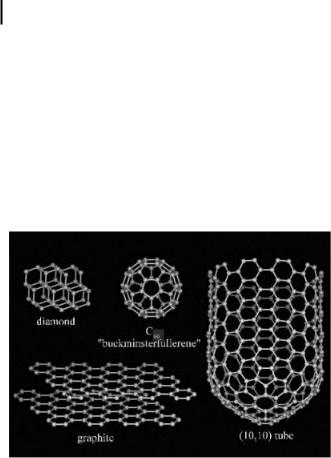
The carbon atoms in graphite, diamond, and fullerenes (C60) are held together by strong covalent bonds. As demonstrated in Fig. 2.1, it is the lattice arrangement of atoms and the type of bonding that differentiate these forms of elemental carbon. Understanding how carbon atoms are arranged in each type of material allows a better understanding of why these compounds have different properties. Notice that graphite, for example, has large sheets of hexagonal honeycomb lattice and strong bonds in these planes. The sheets interact, but they are so far apart (~ 3.35 &) and
Nanofabrication Towards Biomedical Applications. C. S. S. R. Kumar, J. Hormes, C. Leuschner (Eds.) Copyright 2005 WILEY-VCH Verlag GmbH & Co. KGaA, Weinheim
ISBN 3-527-31115-7
34 2 Synthetic Approaches for Carbon Nanotubes
the interactions are via weak Van der Waals force. Because the layers of carbon rings can slide over each other, graphite is a good lubricant. Diamond, however, has each carbon atom bonded to four other carbon atoms in a tetrahedral arrangement. Diamond can be cleaved along its planes, but it cannot flake apart into layers because of this tetrahedral arrangement of carbon atoms. C60, the most important member in the fullerene family, is shaped like a soccer ball, often called a buckyball, reminiscent of the stable geodesic domes that were built by the architect Buckminster Fuller. Perhaps the biggest difference of the fullerenes when compared to their crystalline graphite and diamond counterparts is that the fullerenes are molecular, with exact numbers (60, 70, 82, etc.) of carbon atoms. Fullerenes are discrete entities but can be used as the building blocks of lattices. Carbon nanotubes are extensions of the fullerene structure, as we will discuss later in this chapter.
Figure 2.1. Different crystal carbon structures [1].
2.1.2
Wide Range of Properties
Fullerenes and their derivatives, carbon nanotubes, have triggered extensive and attractive research and promise to be one of the key materials in nanotechnology. Unlike other existing materials, carbon nanomaterials have found many scientific and technological applications in diverse areas, as illustrated in Fig. 2.2. Because of the wide range of superior properties (mechanical, electrical, thermal) that are inherent in carbon nanostructures, specifically nanotubes, and due to the simplicity of their structures (making them good model systems to study physics in nanoscale materials), they play an important role in the current rapid expansion of fundamental studies on nanostructures and potential use in nanotechnology. Based on their dimensions, their novel electronic structures, and their controllable chemical functionality, carbon nanotubes and other carbon nanomaterials are expected to be used in several applications, including medical and biomedical areas, such as drug deliv-
2.2 Family of Carbon Nanomaterials 35
ery and diagnostic devices. In this chapter we will look at the various ways in which carbon nanostructures can be synthesized, with emphasis on nanotubes, and briefly discuss the limitations in these procedures. From here we start with an introduction of members in the carbon nanomaterials family, including fullerenes, nano-onions, nanofibers, nanotubes, nanoscale diamonds and diamond-like carbon and nanoporous activated-carbon (Section 2.2). After a brief summary in Section 2.3 of the main approaches for the synthesis of carbon nanotubes, which are arc discharge, laser ablation, and chemical vapor deposition (CVD), our recent efforts focusing on controllable growth of nanotube architectures based on substrate-site-selective growth by the CVD technique are summarized in Section 2.4. A perspective of nanotubes in medical and bio-medical applications is also presented in Section 2.5, before the conclusion.
Electrical
Engineering
Biology |
|
Information |
Materials |
Carbon |
|
Science |
Chemistry |
|
|
Nanomaterials |
|
Chemical |
|
Physics |
Engineering |
|
|
|
Mechanical |
|
|
Engineering |
|
Figure 2.2. Scientific and technological areas to which carbon nanomaterials research has relevance.
2.2
Family of Carbon Nanomaterials
As briefly mentioned at the beginning of this chapter, the most recently discovered form of crystalline carbon is the fullerene family. Fullerenes were discovered in 1985 [2]. The discovery of C60 led to the discovery of carbon nanotubes in 1991 [3]. Since then, researchers around the world have been exploring both the basic science and potential applications of these novel materials. In this section, the structures and synthesis techniques of several important carbon nanomaterials will be introduced.
2.2.1
Fullerenes
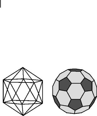
C60 – buckminsterfullerene or the buckyball – involves 60 carbon atoms in a “soccer ball”-shaped structure. The carbon atoms in C60 are arranged in a shell that is made of 20 hexagons and 12 pentagons. This is required by Euler’s theorem, where 12 pentagons
36 2 Synthetic Approaches for Carbon Nanotubes
are required to make a closed shell structure made of a planar hexagonal honeycomb lattice. Larger fullerenes (C70, C82, etc.) have similar structures containing exactly 12 pentagons necessary for closure, but with different numbers of hexagons.
The proposed crystal structure for C60, a truncated icosahedron, is derived from an icosahedron by a snipping process which truncates each of the 12 vertices (see Fig. 2.3). Each vertex is replaced by a five-membered ring, a pentagon. This snipping process also converts each of the 20 original triangular faces into six-membered rings, hexagons. In the proposed structure each of the vertices of the truncated icosahedron is occupied by a carbon atom and each carbon is three-fold-coordinated, similar to the coordination in graphite except for the curvature introduced by the pentagons in the lattice.
a |
b |
Figure 2.3. (a) Icosahedron, (b) truncated icosahedron – C60.
C60 is normally synthesized, as illustrated in Fig. 2.4, by an electrically extracted from the soot produced in the electric arc discharge between two graphite electrodes. Black carbon soot, from which C60 and other fullerenes can be extracted, contains only very small fractions of fullerenes. The extraction is done using organic solvents in which the fullerenes are soluble.
At present there are no practical uses for fullerenes; however, recent research on fullerenes show some prospect of their utilization for medical purposes, such as inhibiting the human immunodeficiency virus (HIV) by attaching fullerenes to the virus and thus preventing its replication [4]. Chemical modifications of the fullerenes into various complexes and adducts could ultimately lead to their applications in the biochemical and pharmaceutical areas.
2.2.2
Carbon Onions (Nested Fullerenes)
Quasi-spherically nested fullerene structures were first reported by Ugarte [5]. Intensive investigations have been carried out to create and image these nested fullerene structures (Fig. 2.5) [6]. Intense electron irradiation of amorphous carbon or graphitic specimens in an electron microscope results first in graphitization (when an
2.2 Family of Carbon Nanomaterials 37
Extinction (Arb. Units) |
|
|
|
|
|
Extinction (Arb. Units) |
|
|
|
|
|
|
400 |
500 |
600 |
700 |
800 |
900 1000 |
400 |
500 |
600 |
700 |
800 |
900 |
1000 |
|
|
Wavelength (nm) |
|
|
Wavelength (nm) |
|
||||||
|
|
|
a |
|
|
|
|
|
b |
|
|
|
Figure 2.4. Contact-arc apparatus used to fabricate macroscopic quantities of C60.
amorphous precursor is irradiated), then curling of the graphene planes and, finally, closure, leaving perfectly spherical concentric-shell graphitic onions. When such an irradiation experiment is carried out at specimen temperatures above 400 C, no defect clustering takes place and the shells of the onions are perfectly coherent. Careful examination of such onions reveals the unique property of self-compression during irradiation. This manifests itself by the reduction of the spacing between the shells below the usual layer spacing of crystalline graphite (0.335 nm). This phenomenon can be explained by the permanent loss of atoms in the outer shells as a
2nm
Figure 2.5. HRTEM image of a carbon onion. (From Ref. [6], with permission.)
result of sputtering by the electron beam. When two adjacent carbon atoms in a shell are missing (a divacancy), the shell can close again by reducing the number of

38 2 Synthetic Approaches for Carbon Nanotubes
faces. Rearrangement via the Stone–Wales transformation can create pentagons and heptagons [7]; an appropriate combination of both ensures the uniform spherical curvature of the onion. The shrinkage of the shells creates a surface tension that tends to make the object spherical and generates pressure within the onion.
A simple method for producing high-quality spherical carbon nano-onions in large quantities without the use of expensive vacuum equipment has been reported recently [8]. The nested onion nanoparticles were generated by arc discharge between two graphite electrodes, similar to the one used for C60 production but submerged in deionized water, that is, in a nonvacuum environment. After the electric discharge the nano-onions remain afloat on the water surface, while the rest of the carbon structures produced fall to the bottom of the beaker, giving material of high purity. The average diameter of the nano-onions is 25–30 nm (range 5–40 nm), a useful size range for many lubrication applications. Nano-onions have been successfully used as an effective catalyst for an important industrial reaction to convert ethylbenzene into styrene [9]. The synthesis of styrene is one of the ten most important industrial chemical processes, and is commonly conducted using a catalyst of potassium-promoted iron oxide (K–Fe) to effect oxidative dehydrogenation of ethylbenzene. This process is thermodynamically limited to a maximum yield of 50%. Carbon onions, in contrast, produce styrene in 62% yield in these preliminary experiments, and the researchers expect further improvement. They think that the key to a still more active catalyst lies in generating an optimal distribution of active sites on the surface of the carbon nano-onions.
2.2.3
Carbon Nanofibers
The term “carbon nanofiber” summarizes a large family of different filamentous nanocarbons. Carbon nanofibers, like carbon nanotubes, are mainly related to graphite structures and their structures have been well investigated [10–12] during the past 50 years or so.
Carbon fibers (micron size structures) have been around for several decades and are commercially important materials. They can be made in a variety of ways, such as by using organic polymers like polyacrylonitrile or by vapor phase deposition with the assistance of catalyst particles (vapor-grown carbon fibers or VGCFs) [13, 14]. The latter are in structure, morphology and degree of graphitization closer to carbon nanofibers.
Proposed models of carbon fiber growth assume that the process usually consists of two steps: first, a high-aspect core filament grows by catalyst-assisted vapor phase growth, and then a (sometimes only partially) graphitized carbon deposition thickens the template structure up to the final dimensions [15–17]. The initial growth stage has been a difficult process to understand. Very recently, however, state-of-the- art transmission electron microscopy equipment has offered the possibility to track the early stages of the nanofiber growth with sufficient spatial and temporal resolution [18, 19]. As shown in Fig. 2.6, the initial equilibrium shape of the catalyst particle (here a Ni particle) transforms into a highly elongated shape. The elongation of
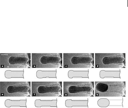
2.2 Family of Carbon Nanomaterials 39
the Ni particle appears to be correlated with the formation of graphene sheets at the graphene–Ni interface with their basal (002) planes oriented parallel to the Ni surface. Hence, the reshaping of the Ni nanocluster assists the alignment of graphene layers into a tubular structure. The elongation of the Ni nanocrystal continues until it reaches a high aspect ratio, before it abruptly contracts to a spherical shape within less than ~0.5 s [Fig. 2.6(h)]. The contraction is attributed to the fact that the increase in the Ni surface energy can no longer be compensated for by the energy gained when binding the graphitic fiber to the Ni surface. The elongation/contraction scenario continues in a periodic manner as the nanofiber grows.
a |
|
b |
|
c |
|
d |
e |
|
f |
|
g |
|
h |
Figure 2.6. Snap images showing a sequence of the growing process of a carbon nanofiber.(From Ref. [19], with permission.)
Carbon nanofibers have various applications and are normally used as fillers to improve the mechanical and thermal properties of composite materials [20]. Other applications include their uses as electrically conducting fillers, as catalyst support, in nanoelectronic devices, as artificial muscles, as field emitters, and in gas and electrochemical energy storage matrices. The production of carbon nanofibers is a mature technology and a 40-ton-per-year commercial plant is already operating in Japan for the production of vapor-grown carbon nanofibers [21].
2.2.4
Carbon Nanotubes
Carbon nanotubes, nanoscale cylinders constructed from sp2 hybridized carbon bonds, form a hexagonal honeycomb lattice as in graphite. Containing a hollow center, carbon nanotubes are derived from graphene sheets that are rolled up into tubes with a seamless structure [22, 23]. The nanotubes are terminated by fullerene endcaps with six pentagons on both ends. The unique mechanical and electrical properties of carbon nanotubes are directly related to the characteristics of the carbon bonds and their organization into the tube lattice. The nanotubes can be distinguished by the number of layers that make up their cylindrical walls: single-walled nanotubes (SWNTs) and multi-walled nanotubes (MWNTs). Figure 2.7 shows mod-
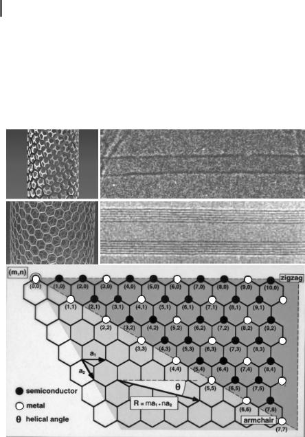
40 2 Synthetic Approaches for Carbon Nanotubes
els and high-resolution transmission electron microscopy (HRTEM) images of a SWNT and a MWNT. Along the tube axis, carbon nanotubes show excellent mechanical properties due to the nature of the strong C–C bonding and the seamless structure. The most intriguing property of carbon nanotubes comes from their unique electronic structure. Depending on the diameter and chirality, carbon nanotubes can be either metallic nanowires with quantum transport property or semiconducting nanomaterials with varying band gaps. They also show good thermal and electrical conductivity, chemical stability, and high mechanical strength. Because of these, carbon nanotubes are promising materials for various applications (for examples, see
a |
b |
c |
d |
e
Figure 2.7. Structures of carbon nanotubes. (a) and (b) are SWNT and (c) and (d) are MWNT. (e) Indices with a pair of integers (n, m) to classify nanotube structures: the white dots denote metallic nanotubes and the black ones are semiconducting nanotubes. (From Ref. [23], with permission.)
2.2 Family of Carbon Nanomaterials 41
Section 2.5) [22–24]. A detailed description of carbon nanotubes synthesis will be presented in Sections 2.3 and 2.4.
2.2.5
Nanoscale Diamonds and Diamond-Like Carbon
Nanocrystalline diamond films are unique new materials with applications in fields as diverse as tribology, cold cathodes, corrosion resistance, electrochemical electrodes, and conformal coatings on microelectromechnical system (MEMS) devices. Man-made diamond crystals were successfully produced in the 1950s by the highpressure, high-temperature method. An alternative method, CVD of diamond at low pressure (typically with the use of an excited CH4/H2 mixture on substrates held at ~700 to 800 C), has also been applied successfully over the last 15–20 years. With the assistance of a double bias, hot-filament CVD was employed to synthesize nanoscale diamonds (Fig. 2.8) [25].
Figure 2.8. HRTEM image of a diamond crystallite (diameter ~6 nm) grown directly on Si with a random alignment. (From Ref. [25], with permission.)
Ultra-nanocrystalline diamond (UNCD) has been synthesized by the modification of the microwave plasma chemical vapor deposition (MPCVD) process [26]. UNCD thin films are synthesized using argon-rich plasmas instead of the hydrogen-rich plasmas normally used to deposit microcrystalline diamond (>1 lm grain size). The use of small amounts of carbon source gases (C60, CH4, C2H2) with argon leads to the formation of C2 dimers, which are the growth species for all UNCD thin films. UNCD grown from C2 precursors consists of ultra-small (2–5 nm) grains and atomically abrupt grain boundaries. These films are superior in many ways to traditional microcrystalline diamond films: they are smooth, dense, pinhole-free, and phasepure, and can be conformally coated on a wide variety of materials and high-aspect- ratio structures. UNCD is finding a wide range of industrial applications in MEMS, as tribo-coatings, as photonic switches in optical cross-connects, as field emission cathodes, as electrochemical electrodes, and as hermetic coatings on bioimplants [26]. With the ability to tailor both the film structure and the electronic properties

42 2 Synthetic Approaches for Carbon Nanotubes
independently, UNCD can be optimized for several important applications. Most excitingly, the ability to electronically dope the material both n- and p-type opens the door to the next generation of novel high-speed, high-temperature, and even biocompatible electronics. In addition to nanocrystalline diamond films, it worth mentioning another form of carbon nanomaterial, diamond-like carbon, which has been evaluated as a coating to improve biocompatibility of orthopedic and cardiovascular implants [27].
2.2.6
Nanoporous Activated Carbon
The surface area of a solid increases when it becomes nanoporous, improving catalytic, absorbent, and adsorbent properties. Activated carbon is an example of a nanoporous material that, like zeolites, has been in use for a long time. Nanoporous carbon consists of very-high-surface-area carbon with a tunable and very narrow pore size distribution. It is suitable in applications such as energy storage systems, catalytic, specific adsorbents, and gas separation. Recent research has developed a templating technique using silica nanoparticles that can create activated carbon with uniform 8-nm and 12-nm pore sizes. The resulting materials show adsorption greater than 10 times that of commercial activated carbon [28]. High surface area of porous carbon materials is ideal for holding dispersed metal catalyst particles for use in heterogeneous catalysis (Fig. 2.9).
Figure 2.9. Atomic level schematics of nanoporous carbon structure with loaded catalyst. (From Ref. [29], with permission.)
Nanoporous carbon membranes prepared by pyrolysis of poly(furfuryl alcohol) on porous stainless steel disks have been investigated for gas separation [30]. The nanoporous carbon molecular sieve membranes can be prepared with very high size and shape selectivity. This offers the opportunity to extend the range of application of carbon membranes beyond surface selective flow. That nanoporous carbon molecular sieves with pore sizes less than 5 & can separate nitrogen from oxygen has been known for some time, and is the basis for nitrogen pressure swing adsorption. The separation, done over packed beds of nanoporous carbon, is based on the kinetics of diffusion rather than on the thermodynamics of adsorption.
2.3 Synthesis of Carbon Nanotubes 43
2.3
Synthesis of Carbon Nanotubes
There are many synthesis methods, such as electric arc, laser ablation chemical vapor deposition, pyrolysis, electrochemical methods, template-based synthesis, flames, and so on, that have been employed to synthesize carbon nanotubes. In this section, three main techniques for the synthesis of carbon nanotubes, both SWNTs and MWNTs, are introduced. They are the arc-discharge method (electric arc), laser ablation (pulsed laser vaporization), and CVD.
2.3.1
Nanotube Growth via the Arc-Discharge Method
Electric arc was the first method reported for producing carbon nanotubes [3] and also the first mass-production technique [31]. For MWNT production two highpurity graphite electrodes are used. During the growth process, nanotubes are formed and deposited on the cathode; the anode is continuously consumed in the process.
Plasma
Graphite rod |
Ni/Y powder |
|
as anode |
||
cathode |
DC power
a
b |
c |
Figure 2.10. (a) Apparatus to produce carbon nanotubes by the electric-arc method.
The setup produces multi-walled nanotubes (MWNTs) when pure carbon rods are applied as electrodes, and produces single-walled
nanotubes (SWNTs) when a metal catalyst is mixed into the core of the anode. (b) Photograph of the cathode deposition; (c) TEM image of the MWNTs.
44 2 Synthetic Approaches for Carbon Nanotubes
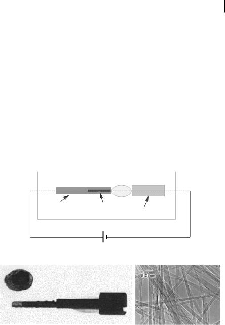
Modifying the method by inserting different metallic catalyst particles into the carbon electrode results in the production of SWNTs [32, 33]. To carry out this experiment the setup is similar to that used for MWNT synthesis, but a small diameter hole is drilled in the anode and packed with a mixture of the metal catalyst and graphite powder (Fig. 2.10). Several metals and combinations of metals have been tried to obtain good yield and quality of nanotubes, and the best so far is a mixture of Ni and Y [34]. After a short growth time (typically several minutes) a network of web-like material containing SWNTs may be collected from the reaction chamber. TEM investigation of the sample reveals organized structures: ropes of nanotubes that consist of tens of SWNTs. The disadvantage of this method is that the samples consist of a considerable amount of non-nanotube carbon contamination and catalyst residue; multistep postsynthesis purification procedures are necessary to obtain clean samples. The mechanism of nanotube formation in the electric arc has not been confirmed, although many speculative models have been proposed [35].
2.3.2
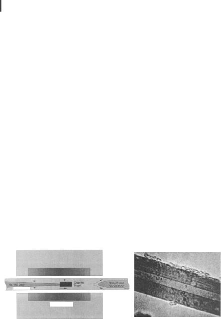
Carbon Nanotubes Produced by Laser Ablation
In the laser ablation technique [ for a schematic see Fig. 2.11(a)] a graphite target is placed in an oven and is ablated with a strong laser pulse in an inert atmosphere. At first, a pure carbon electrode was used at 1200 C ambient temperature of flowing argon gas. The argon carrier gas collects the products and deposits them as soot on a water-cooled substrate [36]. The soot consists of nanotubes with 4–24 layers [Fig. 2.11(b)] and lengths up to 300 nm, accompanied by smaller amounts of onion-like structures. SWNTs were produced only later, when targets were mixed with small percentages (<1 wt%) of catalyst metal (for example Co-Ni powder) [37]. Under optimum conditions, this technique produces large self-assembled SWNT “crystalline” ropes, with lattice (triangular) constant of approximately 17 &. For large-scale pro-
|
|
Graphite |
|
Watercooled |
Nd: YAG Laser |
|
|
||
|
Target |
|
Cu Collector |
|
500 Torr Ar |
|
|||
|
|
|
||
|
|
|
||
|
|
|
||
1200 °C Furnace
a b
Figure 2.11. The first reported experimental apparatus for carbon nanotube production by laser ablation (a), and a MWNT produced in these first experiments (b). (From Ref. [36], with permission.)

2.4 Controllable Synthesis of Carbon Nanotube Architectures 45
duction of SWNTs with high production rates (1.5 g h–1) a high-power free electron laser was used (~200 W power in the experiment) [38].
Despite successful efforts in the last few years to produce larger amounts of nanotubes by the above two high-temperature growth methods, they have not been readily scalable to industrial quantities.
2.3.3
Chemical Vapor Deposition as a Tool for Carbon Nanotube Production
Chemical vapor deposition (CVD) is also an efficient way to grow carbon nanotubes using transition metal particles such as Fe, Co, and Ni as catalysts, and hydrocarbons as carbon precursors. Unlike the arc-discharge and laser ablation approaches, CVD produces carbon nanotubes in a continuous mode and could be scalable to greater amounts of production. At specific temperatures, for example, 650–1000 C, the hydrocarbons, such as CH4, C2H2, benzene, xylene, hexane, and so on, decompose and deposit on the substrate or chamber surfaces. In this method, the carbon nanotubes can grow on the substrate surface randomly or aligned, depending on the growth conditions.
CVD methods can be classified as “hot-wall” or “cold-wall” processes. Hot-wall processes, such as thermal CVD, normally use a high-temperature tube furnace, and the substrate is loaded inside the tube; the whole tube is heated by the furnace in order to heat the substrate to the growth temperature. The hydrocarbon is introduced into the tube and decomposed there. Cold-wall processes, such as a plasmaenhanced CVD, however, only heat the sample by controlling the temperature of the sample holder, leaving the whole system at a relatively low temperature. There are several parameters that have an influence on the growth of carbon nanotubes, for example, growth temperature, carbon source, substrate, catalyst, ratio of catalyst over carbon, and so on.
Among the CVD processes, one unique process, high-pressure CO conversion (HiPCO) synthesis of SWNTs, deserves mention [39]. Instead of using a hydrocarbon as the precursor, this method feeds high-pressure (30–50 atm) carbon monoxide as the carbon source. Relatively large-scale production (10 g per day) of high-purity SWNTs can be obtained by flowing high-pressure CO gas on catalytic clusters of iron, which form in situ from the decomposition of Fe(CO)5 and the condensation of iron atoms.
2.4
Controllable Synthesis of Carbon Nanotube Architectures
In this section, we summarize some of our recent efforts, which are directed towards controlled growth and electrical and structural characterization of aligned nanotubes on planar substrates by CVD. The substrate-site-selective growth [40] of nanotubes allows us to grow well-aligned MWNTs on substrates. This eliminates any catalyst predeposition step in the fabrication process. The fabrication of micro
46 2 Synthetic Approaches for Carbon Nanotubes
and nano electromechanical instruments based on these types of three-dimensional networks of carbon nanotubes may be realized in the future by this approach.
2.4.1
Substrate-Site-Selective Growth
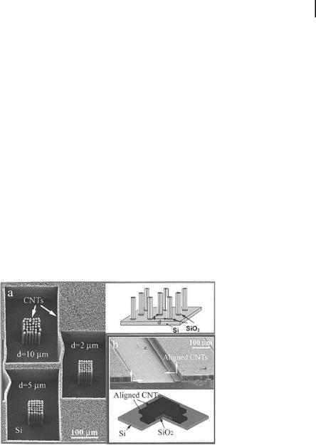
In this specific CVD process we placed predefined SiO2/Si patterns (Fig. 2.12) into a conventional tube furnace. The nanotubes were grown from a mixture of xylene (C8H10) and ferrocene [Fe(C5H5)2]. The reactor is preheated gradually to 800 C and then a 0.01-g ml–1 solution of ferrocene in xylene is preheated to about 150 C and fed into the reactor. In this reaction ferrocene is the nanotube nucleation initiator and xylene is the carbon source. This precursor combination results in highly selective growth of 20to 30-nm-diameter MWNTs on the SiO2 surfaces: no nanotube growth is observed on pristine Si surfaces or on the native oxide layer. The film is comprised of vertically aligned nanotubes with center-to-center average spacing of ~50 nm [41].
To reveal the reason for this strong substrate selectivity we investigated the mechanism of catalyst particle formation on different substrates. Particles are formed and deposited both on silicon and silica surfaces, with a size around 20–40 nm in the silicon oxide region and slightly bigger in the Si region. Measurements made by an
SiO2 layer
Si
Photo-Resist
Developing
Etching
SiO2/Si Patterns
Growth of Nanotubes
a
Figure 2.12. The process used to create silica patterns on a silicon substrate. (a) The sequence from top to bottom: generation of a SiO2 layer on a Si wafer; spin coating of a photoresist; photoexposure through a mask
b
and resist development; etching the exposed SiO2; photoresist removal and growth of nanotubes on the patterned SiO2 surface.
(b) Patterned MWNT layers.
2.4 Controllable Synthesis of Carbon Nanotube Architectures 47
electron probe microanalyzer and by Auger electron spectroscopy showed that iron and carbon are dispersed over both regions. Cross-sectional TEM observation of the substrates showed that particles on the top of silicon oxide surfaces are pure gamma iron (fcc Fe), which is an active catalyst for carbon nanotube growth. However, on the silicon surface iron silicide is formed by substrate particle interactions, and these silicide phases are not effective catalysts [42].
2.4.2
Three-Dimensional Nanotube Architectures
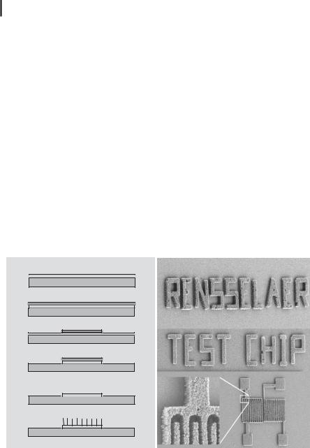
The site selectivity of the floating catalyst CVD method is a powerful tool to design mesoscale structures similar to ones used as MEMS. To demonstrate this possibility we carried out simultaneous multidirectional growth and multilayered growth of ordered nanotubes [43, 44]. To provide depth for the horizontal growth, thick silica layers were deposited by plasma-enhanced CVD (PECVD) to create high-aspect-ratio silica features. Patterns of Si/SiO2 of various shapes were generated by photolithography followed by a combination of wet and/or dry etching. CVD growth of nanotubes is stimulated in a manner similar to the above-described method using a xylene/ferrocene mixture (Fig. 2.13). With this method nanotube growth in mutually orthogonal directions and growth with oblique inclinations (that is, neither orthogonal nor planar with respect to the substrate plane) has been illustrated [44].
Figure 2.13. Carbon nanotube structures deposited on patterned, three-dimensional silicon/silica templates. The length of the nanotubes in both vertical and horizontal directions
is about 60 mm. The thickness of the patterned SiO2 layer was 8.5 mm in the presented experiment. (From Ref. [43], with permission.)
482 Synthetic Approaches for Carbon Nanotubes
2.4.3
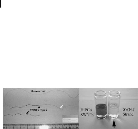
Super-Long SWNT Strands
Mesostructures of SWNTs can also be grown by techniques involving vapor phase catalyst delivery, similar to the above. We have synthesized long strands of ordered SWNTs (Fig. 2.14) by a CVD deposition technique with the floating catalyst method,
but in a vertical furnace, using n-hexane as a carbon source [45, 46]. The n-hexane solution with ferrocene content of 0.018 g ml–1 and thiophene of 0.4 wt% was introduced into the reactor after heating the reactor to the pyrolysis temperature
(~1100 C), using hydrogen as carrier gas. In the process SWNTs formed in abundance with yields of ~0.5 g h–1. The formation of very long SWNT strands, also in large amounts (approximately 20–30% of the product), is the unique characteristic of this vertical floating process. The SWNT strands consist of smaller-diameter ropes, which also seem very long, almost as long as the strand itself (several inches) and can be manually handled quite easily.
a |
b |
Figure 2.14. (a) Nanotube strand made of the longest SWNT produced to date. (b) Comparison of two samples of similar mass (HiPCO and the long strands) ultrasonicated in ethanol.
Raman spectra taken from different areas along the strands are very similar to each other, indicating homogeneity along the strands. The diameter of SWNTs determined from the frequency of the radial breathing modes (RBM) is in the range of 1.1–1.7 nm, with a dominance of tubes of 1.1 nm, in accordance with our TEM investigations. Measurements were directly conducted on these strands, namely direct tensile test and electrical measurements. The stress in the strands was recorded on individual SWNT strands of centimeter lengths, of diameter 5–20 mm. Modulus values obtained directly from the measurements were 49–77 GPa, smaller than what is predicted for individual nanotubes but still of relatively large magnitude compared to existing fibers. Macroscopic electrical resistivity of nanotube strands was measured from room temperature to 5K using a four-probe method. The crossover temperature from metallic to semiconducting state occurred at about 90K. The metallic resistivity is about six times the value of single bundles reported previously but less than any other macroscopic SWNT structures, suggesting continuous conducting paths along the long nanotube strands.
2.5 Perspective on Biomedical Applications 49
Double-walled carbon nanotubes (DWNTs) have been brought to the forefront of research in recent years in the nanotube community due to the fact that they are at the frontier between SWNTs and MWNTs and could have the advantages of both. They open a possibility of functionalizing the outer wall, which will ensure connections with the external environment, while retaining the remarkable mechanical and electronic properties of the inner nanotube. This may prove to be very useful for their integration into systems and composites. DWNTs were first reported using pyrolytic organic precursor [47] and recently have been synthesized using the arc-dis- charge [48] and the CVD techniques [49].
2.5
Perspective on Biomedical Applications
Due to the fact that carbon nanomaterials, particularly carbon nanotubes, have novel structures, small and well-defined dimensions paired with extremely high electrical and thermal conductivity, high mechanical strength and flexibility, as discussed before, various prospective applications of nanotubes have been proposed such as nanoelectronic devices, energy storage, nanocomposites, nanosensors, and so on. A detailed review of this aspect can be found in Refs. [22–24]. Considering the scope of this book we will just give a brief perspective on nanotubes in biomedical applications, one of their key future areas of application.
2.5.1
Imaging and Diagnostics
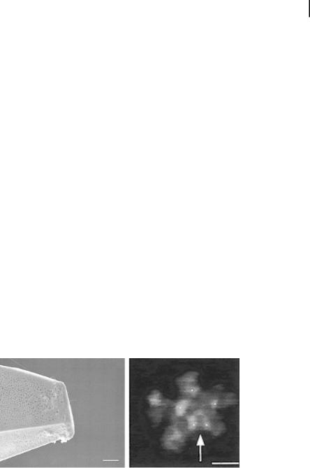
A striking example is shown in Fig. 2.15, using an individual MWNT attached to the end of a scanning probe microscope tip for imaging biomolecules [50]. The advantage of the nanotube tip is its slenderness and the ability to image features (such as very small, deep surface cracks) which are almost impossible to probe using the
10 nm
a |
b |
Figure 2.15. Individual MWNT grown directly onto an AFM tip
(a) and a picture to demonstrate its lateral resolution (b). (From Ref. [50], with permission.)
50 2 Synthetic Approaches for Carbon Nanotubes
larger, blunter-etched Si or metal tips. Biological molecules such as DNA can readily be imaged at higher resolution using nanotube tips than with conventional scanning tunneling microscope tips. MWNT and SWNT tips were used in a tapping mode to image biological molecules such as amyloid-b-protofibrils (related to Alzheimer’s disease) with a resolution never achieved before.
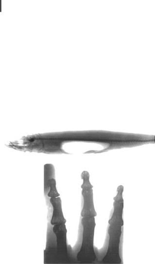
Another example of medical diagnostic imaging is x-ray radiation coming from a nanotube x-ray source [51]. The basic design of the x-ray tube has not changed significantly in the last century. The x-ray intensity generated using a carbon nanotube (CNT)-based field-emission cathode is sufficient to image a human extremity (Fig. 2.16). The device can readily produce both continuous and pulsed x-rays with a programmable wave form and repetition rate. Pulsed x-ray with a repetition rate greater than 100 kHz was readily achieved by programming the gate voltage. The CNT-based cold-cathode x-ray technology can potentially lead to portable and miniature x-ray sources for industrial and medical applications.
a
b
Figure 2.16. X-ray images of a fish (a) and a humanoid hand
(b) taken using the nanotube x-ray source. Detailed bone structures are clearly resolved. (From Ref. [51], with permission.)
2.5.2
Biosensors
Carbon nanotubes can be used for monitoring enzyme activity. Immobilization of proteins on the sidewall of carbon nanotubes through a linking molecule has already been demonstrated [52]. Proteins carrying pH-dependent charged groups that can electrostatically gate a semiconducting SWNT created the possibility to construct a nanosize protein and/or pH sensor. Redox enzymes go through a catalytic
2.5 Perspective on Biomedical Applications 51
reaction cycle where groups in the enzyme temporarily change their charge state and conformational changes occur in the enzyme. This enzymatic activity can potentially be monitored with a nanotube sensor. Figure 2.17 demonstrates the use of individual semiconducting SWNTs as versatile biosensors [53]. Controlled attachment of the redox enzyme glucose oxidase (GOx) to the nanotube sidewall is achieved through a linking molecule and is found to induce a clear change of the conductance. The enzyme-coated tube is found to act as a pH sensor with large and reversible changes in conductance upon changes in pH. Upon addition of glucose, the substrate of GOx, a steplike response can be monitored in real time, indicating that the sensor is capable of measuring enzymatic activity at the level of a single nanotube. This demonstration of nanotube-based biosensors provides a new tool for enzymatic studies and opens the way to biomolecular diagnostics.
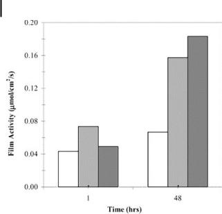
Another approach has been explored using enzyme-containing polymer-SWNT composites as unique biocatalytic materials [54]. The biocatalytic composites were prepared by suspending SWNT and a-chymotrypsin (CT) directly into a poly(methyl methacrylate) solution in toluene. The activity of the resulting CT-polymer-nanotube films was observed to be higher than both polymer-CT and polymer-graphite-CT films. SWNT-containing composites show higher enzyme activity than the non-
a
b
Figure 2.17. (a) Two electrodes connecting a semiconducting SWNT with GOx enzymes immobilized on its surface. (b) Conductance of a semiconducting SWNT as a function of the liquid-gate voltage in water. Data are for the
bare SWNT (I), after 2 h in dimethylformamide with/without the linking molecule (II), and after GOx immobilization (III). (From Ref. [53], with permission.)
52 2 Synthetic Approaches for Carbon Nanotubes
|
|
|
|
|
|
|
|
|
|
|
|
|
|
|
|
|
|
|
|
|
|
|
|
|
|
|
|
|
|
|
|
|
|
|
|
|
|
|
|
|
|
|
|
|
|
|
|
|
|
|
|
|
|
|
|
|
|
|
|
|
|
|
|
|
|
|
|
|
|
|
|
|
|
|
|
|
|
|
|
|
|
|
|
|
|
|
|
|
|
|
|
|
|
|
|
|
|
|
|
|
|
|
|
|
|
|
|
|
|
|
|
|
|
|
|
|
|
|
|
|
|
|
|
|
|
|
|
|
|
|
|
|
|
|
|
|
|
|
|
|
|
|
|
|
|
|
|
|
|
|
|
|
|
|
|
|
|
|
|
|
|
|
|
|
|
|
|
|
|
|
|
|
|
|
|
|
|
|
|
|
|
|
|
|
|
|
|
|
|
|
|
|
|
|
|
|
|
|
|
|
|
|
|
|
|
|
|
|
|
|
|
|
|
|
|
|
|
|
|
|
|
|
|
|
|
|
|
|
|
|
|
|
|
|
|
|
|
|
|
|
|
|
|
|
|
|
|
|
|
|
|
|
|
|
|
|
|
|
|
|
|
|
|
|
|
|
|
|
|
|
|
|
|
|
|
|
|
|
|
|
|
|
|
|
|
|
|
|
|
|
|
|
|
|
|
|
|
|
|
|
|
|
|
|
|
|
|
|
|
|
|
|
|
|
|
|
|
|
|
|
|
|
|
|
|
|
|
|
|
|
|
|
|
|
|
|
|
|
|
|
|
|
|
|
|
|
|
|
|
|
|
|
|
|
|
|
|
|
|
|
|
|
|
|
|
|
|
|
|
|
|
|
|
|
|
|
|
|
|
|
|
|
|
|
|
|
|
|
|
|
|
|
|
|
|
|
|
|
|
|
|
|
|
|
|
|
|
|
|
|
|
|
|
|
|
|
|
|
|
|
|
|
|
|
Figure 2.18. Comparison of biocatalytic film |
5 mg SWNT; each with 1 mg CT and 1.0 g |
|||||||||||||||||||||||
activities of poly(methyl methacrylate)-a-chy- |
poly(methyl methacrylate). (From Ref. [25], |
|||||||||||||||||||||||
motrypsin-SWNT composites. White bar, 1 mg |
with permission.) |
|||||||||||||||||||||||
SWNT; hatched bar, 2 mg SWNT; black bar, |
|
|
|
|
|
|
|
|
|
|||||||||||||||
SWNT preparations, indicating that SWNTs may be used to improve the performance of a wide range of biocatalytic composites for applications ranging from antifouling surface coatings to sensor elements.
2.6
Conclusion
Due to the rapid growth of the field we could only briefly summarize the synthesis achievements of carbon nanomaterials. We have presented some results regarding chemical vapor deposition of nanotubes with a wide variety of relations to their growth environment. Most of the applications require not only the nanotubes themselves but handling them as parts of bigger systems, consisting in most cases of great numbers of nano-objects and their interconnects. On specific templates we were able to control the nanotubes’ growth in three dimensions, resulting in structures that could be applicable later in electronic circuitry or MEMS devices to create nanotube-based devices (diodes, transistors, RAM elements) with predefined properties, high yield, and in high density for biomedical diagnostics and medical applications. The promise of such nanomaterials in biomedical applications, particularly carbon nanotubes, used as nanoprobes in the applications of high-resolution imaging and biosensors, is obvious.

References 53
Acknowledgments
The authors would like to thank all the collaborators at Rensselaer Polytechnic Institute and Tsinghua University. B.Q.W. acknowledges financial support from Louisiana State University Council on Research.
Abbreviations
CNT – carbon nanotube
CT – a-chymotrypsin
CVD – chemical vapor deposition
DWNT – double-walled carbon nanotube
EPMA – electron probe microanalyzer
GOx – glucose oxidase
HiPCO – high pressure CO conversion method
HRTEM – high-resolution transmission electron microscopy
MEMS – microelectromechnical system
MPCVD – microwave plasma chemical vapor deposition
MWNT – multi-walled carbon nanotube
PECVD – plasma-enhanced chemical vapor deposition
SWNT – single-walled carbon nanotube
TEM – transmission electron microscopy
UNCD – ultra-nanocrystalline diamond
VGCF – vapor-grown carbon fiber
References
1 www.plaza.snu.ac.kr/~seongkim/ cnt/
2H. W. Kroto, J. R. Heath, S. C. Obrien, et al., C60 – Buckminsterfullerene, Nature 1985,
318, 162–163.
3S. Iijima, Helical microtubules of graphitic carbon, Nature 1991, 354, 56–58.
4S. H. Friedman, D. L. Decamp, R. P. Sijbesma, et al., Inhibition of the HIV-1 protease by fullerene derivatives – model-building studies and experimental verification, J. Am. Chem. Soc. 1993, 115, 6506–6509.
5D. Ugarte, Curling and closure of graphitic networks under electron-beam irradiation,
Nature 1992, 359, 707–709.
6F. Banhart, Irradiation effects in carbon nanostructures, Reports Prog. Phys. 1999, 62, 1181–1221.
7A. J. Stone, D. J. Wales, Theoretical-studies of icosahedral C60 and some related species,
Chem. Phys. Lett. 1986, 128, 501–503.
8N. Sano, H. Wang, M. Chhowalla, et al., Nanotechnology – synthesis of carbon onions’ in water, Nature 2001, 414, 506–507.
9N. Keller, N. I. Maksimova, V. V. Roddatis, et al., The catalytic use of onion-like carbon materials for styrene synthesis by oxidative dehydrogenation of ethylbenzene, Angew.
Chem. Intl. Edn. 2002, 41, 1885–1888.
10W. R. Davis, R. J. Slawson, G. R. Rigby, An unusual form of carbon, Nature 1953, 171, 756.
11T. Baird, J. R. Fryer, B. Grant, Structure of fibrous carbon, Nature 1971, 233, 329–330.
12Y. X. Zhao, C. W. Bowers, I. L. Spain, Graphitic nature of chemical vapor-deposited carbon filaments grown on silicon surfaces from acetylene, Carbon 1988, 26, 291–293.

54 2 Synthetic Approaches for Carbon Nanotubes
13M. Endo, Y. A. Kim, T. Matusita, T. Hayashi, From vapor-grown carbon fibers (VGCFs) to carbon nanotubes, in Carbon Filaments and Nanotubes: Common Origins, Differing Applications? eds. L. P. Biro, C. A. Bernardo,
G.G. Tibbetts, Ph. Lambin, Kluwer Academic Publishers, Dordrecht, Boston, London, 2000.
14M. Bognitzki, W. Czado, T. Frese, et al., Nanostructured fibers via electrospinning, Adv. Mater. 2001, 13, 70–72.
15G. G. Tibbetts, Nucleation and growth of carbon filaments and vapor grown carbon fibers, in Carbon Filaments and Nanotubes: Common Origins, Differing Applications? eds. L. P. Biro,
C.A. Bernardo, G. G. Tibbetts, Ph. Lambin, Kluwer Academic Publishers, Dordrecht, Boston, London, 2000.
16R. T. K. Baker, P. S. Harris, The formation of filamentous carbon, in Chemistry and Physics of Carbon, eds. P. L. Walker, P. A. Thrower, Dekker, New York, 1978.
17M. Endo, K. Takeuchi, K. Kobori, et al., Pyrolytic carbon nanotubes from vapor-grown car- bon-fibers, Carbon 1995, 33, 873–881.
18P. M. Ajayan, Nanotechnology – how does a nanofibre grow? Nature 2004, 427, 402–403.
19S. Helveg, C. L+pez-Cartes, J. Sehested, et al., Atomic-scale imaging of carbon nanofibre growth, Nature 2004, 427, 426–429.
20J. P. Issi, B. Nysten, Electrical and thermal transport properties in carbon fibers, in Carbon Fibers, eds. J. B. Donnet, S. Rebouillat,
T.K. Wang, J. C. M. Peng, Marcel Dekker, New York, 1998.
21www.japancorp.net/Article.Asp?Art_ID=5719
22P. M. Ajayan, Nanotubes from carbon, Chem. Rev. 1999, 99, 1787–1799.
23M. S. Dresselhaus, G. Dresselhaus,
P.Avouris, Carbon Nanotubes: Synthesis, Structure, Properties, and Applications, Springer, Berlin, New York, 2001.
24R. H. Baughman, A. A. Zakhidov,
W.A. de Heer, Carbon nanotubes – the route toward applications, Science 2002, 297, 787–792.
25S. T. Lee, H. Y. Peng, X. T. Zhou, et al., A nucleation site and mechanism leading to epitaxial growth of diamond films, Science 2000,
287, 104–106.
26D. M. Gruen, Nanocrystalline diamond films,
Ann. Rev. Mater. Sci. 1999, 29, 211–259.
27A. Singh, G. Ehteshami, S. Massia, et al., Glial cell and fibroblast cytotoxicity study on plasma-deposited diamond-like carbon coatings, Biomaterials 2003, 24, 5083–5089.
28S. J. Han, K. Sohn, T. Hyeon, Fabrication of new nanoporous carbons through silica templates and their application to the adsorption of bulky dyes, Chem. Mater. 2000, 12, 3337–3341.
29P. M. Ajayan, I. S. Schadler, P. V. Braun,
Nanocomposite Science and Technology, WileyVCH, Weinheim, Germany, 2003.
30M. Acharya, H. C. Foley, Transport in nanoporous carbon membranes: experiments and analysis, AICHE J. 2000, 46, 911–922.
31T. W. Ebbesen, P. M. Ajayan, Large-scale synthesis of carbon nanotubes, Nature 1992, 358, 220–221.
32S. Iijima, T. Ichihashi, Single-shell carbon nanotubes of 1-nm diameter, Nature 1993, 363, 603–605.
33D. S. Bethune, C. H. Kiang, M. S. de Vries, et al., Cobalt-catalyzed growth of carbon nanotubes with single-atomic-layer walls, Nature 1993, 363, 605–607.
34C. Journet, W. K. Maser, P. Bernier, et al., Large-scale production of single-walled carbon nanotubes by the electric-arc technique, Nature 1997, 388, 756–758.
35L. B. Kiss, R. Vajtai, P. M. Ajayan, Random walk in gas vortices and nanotube self-assem- bly, Phys. Status Solidi (b) 1999, 214(1), R3–R4.
36T. Guo, P. Nikoleav, A. G. Rinzler, et al., Selfassembly of tubular fullerenes, J. Phys. Chem. 1995, 99, 10694–10697.
37A. Thess, R. Lee, P. Nikolaev, et al., Crystalline ropes of metallic carbon nanotubes,
Science 1996, 273, 483–487.
38P. C. Eklund, B. K. Pradhan, U. J. Kim, et al., Large-scale production of single-walled carbon nanotubes using ultrafast pulses from a free electron laser, Nano Lett. 2002, 2, 561–566.
39P. Nikolaev, M. J. Bronikowski, R. K. Bradley, et al., Gas-phase catalytic growth of singlewalled carbon nanotubes from carbon monoxide, Chem. Phys. Lett. 1999, 313, 91–97.
40Z. J. Zhang, B. Q. Wei, G. Ramanath,
P. M. Ajayan, Substrate-site selective growth of aligned carbon nanotubes, Appl. Phys. Lett. 2000, 77, 3764–3766.

41J. T. Drotar, B. Q. Wei, Y. P. Zhao, et al., Reflection high-energy electron diffraction from carbon nanotubes, Phys. Rev. B 2001, 64, 125417.
42Y. J. Jung, B. Q. Wei, R. Vajtai, et al., Mechanism of selective growth of carbon nanotubes on SiO2/Si patterns, Nano Lett. 2003, 3, 561–564.
43B. Q. Wei, R. Vajtai, Y. Jung, et al., Organized assembly of carbon nanotubes – cunning refinements help to customize the architecture of nanotube structures, Nature, 2002, 416, 495–496.
44B. Q. Wei, R. Vajtai, Y. Jung, et al., Assembly of highly organized carbon nanotube architectures by chemical vapor deposition, Chem. Mater., 2003, 15, 1598–1606.
45H. W. Zhu, C. L. Xu, D. H. Wu, et al., Direct synthesis of long single-walled carbon nanotube strands, Science 2002, 296, 884–886.
46B. Q. Wei, R. Vajtai, Y. Y. Choi, et al., Structural characterizations of long single-walled carbon nanotube strands, Nano Lett. 2002, 2, 1105–1107.
47A. Sarkar, H. W. Kroto, M. Endo, Hemi-toro- idal networks in pyrolytic carbon nanotubes,
Carbon 1995, 33, 51–55.
References 55
48J. L. Hutchison, N. A. Kiselev,
E. P. Krinichnaya, et al., Double-walled carbon nanotubes fabricated by a hydrogen arc discharge method, Carbon 2001, 39, 761–770.
49A. Peigney, P. Coquay, E. Flahaut, et al., A study of the formation of singleand double-walled carbon nanotubes by a CVD method, J. Phys. Chem. B 2001, 105, 9699–9710.
50J. H. Hafner, C. L. Cheung, C. M. Lieber, Growth of nanotubes for probe microscopy tips, Nature 1999, 398, 761.
51G. Z. Yue, Q. Qiu, B. Gao, et al., Generation of continuous and pulsed diagnostic imaging x-ray radiation using a carbon-nanotube- based field-emission cathode, Appl. Phys. Lett. 2002, 81, 355–357.
52R. J. Chen, Y. Zhang, D. Wang, H. Dai, Noncovalent sidewall functionalization of singlewalled carbon nanotubes for protein immobilization, J. Am. Chem. Soc. 2001, 123, 3838.
53K. Besteman, J.O. Lee, F.G.M. Wiertz, et al., Enzyme-coated carbon nanotubes as singlemolecule biosensors, Nano Lett. 2003, 3, 727–730.
54K. Rege, N. R. Raravikar, D. Y. Kim, et al., Enzyme-polymer-single walled carbon nanotube composites as biocatalytic films, Nano Lett. 2003, 3, 829–832.