

MAX 7000 Programmable Logic Device Family Data Sheet
Design Security
Generic Testing
All MAX 7000 devices contain a programmable security bit that controls access to the data programmed into the device. When this bit is programmed, a proprietary design implemented in the device cannot be copied or retrieved. This feature provides a high level of design security because programmed data within EEPROM cells is invisible. The security bit that controls this function, as well as all other programmed data, is reset only when the device is reprogrammed.
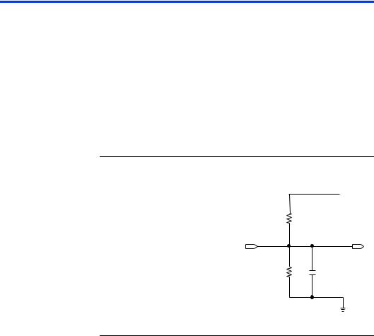
Each MAX 7000 device is functionally tested. Complete testing of each programmable EEPROM bit and all internal logic elements ensures 100% programming yield. AC test measurements are taken under conditions equivalent to those shown in Figure 10. Test patterns can be used and then erased during early stages of the production flow.
Figure 10. MAX 7000 AC Test Conditions
Power supply transients can affect AC measurements. Simultaneous transitions of multiple outputs should be avoided for accurate measurement. Threshold tests must not be performed under AC conditions. Large-amplitude, fast ground-current transients normally occur as the device outputs discharge the load capacitances. When these transients flow through the parasitic inductance between the device ground pin and the test system ground, significant reductions in observable noise immunity can result. Numbers in brackets are for 2.5-V devices and outputs. Numbers without brackets are for 3.3-V devices and outputs.
|
VCC |
464 Ω |
|
[703 |
Ω] |
Device |
To Test |
Output |
System |
250 Ω
[8.06 KΩ] C1 (includes JIG capacitance)
Device input
rise and fall times < 3 ns
QFP Carrier &
Development
Socket
MAX 7000 and MAX 7000E devices in QFP packages with 100 or more pins are shipped in special plastic carriers to protect the QFP leads. The carrier is used with a prototype development socket and special programming hardware available from Altera. This carrier technology makes it possible to program, test, erase, and reprogram a device without exposing the leads to mechanical stress.
f For detailed information and carrier dimensions, refer to the QFP Carrier & Development Socket Data Sheet.
1 MAX 7000S devices are not shipped in carriers.
Altera Corporation |
25 |

MAX 7000 Programmable Logic Device Family Data Sheet
Operating
Conditions
Tables 13 through 18 provide information about absolute maximum ratings, recommended operating conditions, operating conditions, and capacitance for 5.0-V MAX 7000 devices.
Table 13. MAX 7000 5.0-V Device Absolute Maximum Ratings |
Note (1) |
|
|
|
|
|
|
||
|
|
|
|
|
|
|
|
|
|
Symbol |
Parameter |
Conditions |
|
Min |
|
Max |
|
Unit |
|
|
|
|
|
|
|
|
|
|
|
VCC |
Supply voltage |
With respect to ground (2) |
|
–2.0 |
7.0 |
|
|
V |
|
|
|
|
|
|
|
|
|
|
|
VI |
DC input voltage |
|
|
–2.0 |
7.0 |
|
|
V |
|
IOUT |
DC output current, per pin |
|
|
–25 |
25 |
|
mA |
||
TSTG |
Storage temperature |
No bias |
|
–65 |
150 |
|
° C |
||
TAMB |
Ambient temperature |
Under bias |
|
–65 |
135 |
|
° C |
||
TJ |
Junction temperature |
Ceramic packages, under bias |
|
|
150 |
|
° C |
||
|
|
PQFP and RQFP packages, under bias |
|
135 |
|
° C |
|||
|
|
|
|
|
|
|
|
|
|
|
|
|
|
|
|
|
|||
Table 14. MAX 7000 5.0-V Device Recommended Operating Conditions |
|
|
|
|
|
|
|||
|
|
|
|
|
|
|
|
|
|
Symbol |
Parameter |
Conditions |
|
Min |
|
Max |
|
Unit |
|
|
|
|
|
|
|
|
|
|
|
VCCINT |
Supply voltage for internal logic and |
(3), (4), (5) |
|
4.75 |
|
5.25 |
|
V |
|
|
input buffers |
|
|
(4.50) |
|
(5.50) |
|
|
|
|
|
|
|
|
|
|
|
|
|
VCCIO |
Supply voltage for output drivers, |
(3), (4) |
|
4.75 |
|
5.25 |
|
V |
|
|
5.0-V operation |
|
|
(4.50) |
|
(5.50) |
|
|
|
|
|
|
|
|
|
|
|
|
|
|
Supply voltage for output drivers, |
(3), (4), (6) |
|
3.00 |
|
3.60 |
|
V |
|
|
3.3-V operation |
|
|
(3.00) |
|
(3.60) |
|
|
|
|
|
|
|
|
|
|
|
|
|
VCCISP |
Supply voltage during ISP |
(7) |
|
4.75 |
|
5.25 |
|
V |
|
VI |
Input voltage |
|
|
–0.5 (8) |
|
VCCINT + 0.5 |
V |
||
VO |
Output voltage |
|
|
0 |
|
VCCIO |
|
V |
|
TA |
Ambient temperature |
For commercial use |
|
0 |
|
70 |
|
|
° C |
|
|
For industrial use |
|
–40 |
|
85 |
|
|
° C |
|
|
|
|
|
|
|
|
|
|
TJ |
Junction temperature |
For commercial use |
|
0 |
|
90 |
|
|
° C |
|
|
For industrial use |
|
–40 |
|
105 |
|
|
° C |
|
|
|
|
|
|
|
|
|
|
tR |
Input rise time |
|
|
|
|
40 |
|
|
ns |
tF |
Input fall time |
|
|
|
|
40 |
|
|
ns |
26 |
Altera Corporation |

MAX 7000 Programmable Logic Device Family Data Sheet
Table 15. MAX 7000 5.0-V Device DC Operating Conditions Note (9)
Symbol |
Parameter |
Conditions |
|
Min |
Max |
Unit |
|
|
|
|
|
|
|
VIH |
High-level input voltage |
|
|
2.0 |
VCCINT + 0.5 |
V |
VIL |
Low-level input voltage |
|
|
–0.5 (8) |
0.8 |
V |
VOH |
5.0-V high-level TTL output voltage |
IOH = –4 mA DC, VCCIO = 4.75 V (10) |
|
2.4 |
|
V |
|
3.3-V high-level TTL output voltage |
IOH = –4 mA DC, VCCIO = 3.00 V (10) |
|
2.4 |
|
V |
|
3.3-V high-level CMOS output |
IOH = –0.1 mA DC, VCCIO = 3.0 V (10) |
VCCIO – 0.2 |
|
V |
|
|
voltage |
|
|
|
|
|
|
|
|
|
|
|
|
VOL |
5.0-V low-level TTL output voltage |
IOL = 12 mA DC, VCCIO = 4.75 V (11) |
|
|
0.45 |
V |
|
3.3-V low-level TTL output voltage |
IOL = 12 mA DC, VCCIO = 3.00 V (11) |
|
|
0.45 |
V |
|
3.3-V low-level CMOS output |
IOL = 0.1 mA DC, VCCIO = 3.0 V(11) |
|
|
0.2 |
V |
|
voltage |
|
|
|
|
|
|
|
|
|
|
|
|
II |
Leakage current of dedicated input |
VI = –0.5 to 5.5 V (11) |
|
–10 |
10 |
μA |
|
pins |
|
|
|
|
|
|
|
|
|
|
|
|
IOZ |
I/O pin tri-state output off-state |
VI = –0.5 to 5.5 V (11), (12) |
|
–40 |
40 |
μA |
|
current |
|
|
|
|
|
|
|
|
|
|
|
|
|
|
|
|
|||
Table 16. MAX 7000 5.0-V Device Capacitance: EPM7032, EPM7064 & EPM7096 Devices |
Note (13) |
|||||
|
|
|
|
|
|
|
Symbol |
Parameter |
Conditions |
|
Min |
Max |
Unit |
|
|
|
|
|
|
|
CIN |
Input pin capacitance |
VIN = 0 V, f = 1.0 MHz |
|
|
12 |
pF |
CI/O |
I/O pin capacitance |
VOUT = 0 V, f = 1.0 MHz |
|
|
12 |
pF |
|
|
|
|
|
||
Table 17. MAX 7000 5.0-V Device Capacitance: MAX 7000E Devices |
Note (13) |
|
|
|||
|
|
|
|
|
|
|
Symbol |
Parameter |
Conditions |
|
Min |
Max |
Unit |
|
|
|
|
|
|
|
CIN |
Input pin capacitance |
VIN = 0 V, f = 1.0 MHz |
|
|
15 |
pF |
CI/O |
I/O pin capacitance |
VOUT = 0 V, f = 1.0 MHz |
|
|
15 |
pF |
|
|
|
|
|
||
Table 18. MAX 7000 5.0-V Device Capacitance: MAX 7000S Devices |
Note (13) |
|
|
|||
|
|
|
|
|
|
|
Symbol |
Parameter |
Conditions |
|
Min |
Max |
Unit |
|
|
|
|
|
|
|
CIN |
Dedicated input pin capacitance |
VIN = 0 V, f = 1.0 MHz |
|
|
10 |
pF |
CI/O |
I/O pin capacitance |
VOUT = 0 V, f = 1.0 MHz |
|
|
10 |
pF |
Altera Corporation |
27 |
MAX 7000 Programmable Logic Device Family Data Sheet
Notes to tables:
(1)See the Operating Requirements for Altera Devices Data Sheet.
(2)Minimum DC input voltage on I/O pins is –0.5 V and on 4 dedicated input pins is –0.3 V. During transitions, the inputs may undershoot to –2.0 V or overshoot to 7.0 V for input currents less than 100 mA and periods shorter than 20 ns.
(3)Numbers in parentheses are for industrial-temperature-range devices.
(4)VCC must rise monotonically.
(5)The POR time for all 7000S devices does not exceed 300 μs. The sufficient VCCINT voltage level for POR is 4.5 V. The device is fully initialized within the POR time after VCCINT reaches the sufficient POR voltage level.
(6)3.3-V I/O operation is not available for 44-pin packages.
(7)The VCCISP parameter applies only to MAX 7000S devices.
(8)During in-system programming, the minimum DC input voltage is –0.3 V.
(9)These values are specified under the MAX 7000 recommended operating conditions in Table 14 on page 26.
(10)The parameter is measured with 50% of the outputs each sourcing the specified current. The IOH parameter refers to high-level TTL or CMOS output current.
(11)The parameter is measured with 50% of the outputs each sinking the specified current. The IOL parameter refers to low-level TTL, PCI, or CMOS output current.
(12)When the JTAG interface is enabled in MAX 7000S devices, the input leakage current on the JTAG pins is typically –60 μA.
(13)Capacitance is measured at 25° C and is sample-tested only. The OE1 pin has a maximum capacitance of 20 pF.
Figure 11 shows the typical output drive characteristics of MAX 7000 devices.
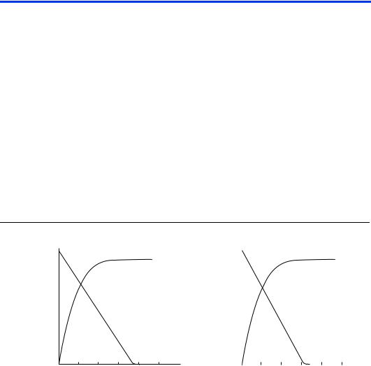
Figure 11. Output Drive Characteristics of 5.0-V MAX 7000 Devices
|
150 |
|
|
|
|
|
IOL |
|
|
|
150 |
|
|
|
IOL |
|
|
|
|
|
|
|
|
|
|
|
|
|
|
|
|
|
|||||||
|
|
|
|
|
|
|
|
|
|
|
|
|
|
|
|
|
|||
Typical I O |
120 |
|
|
|
|
|
|
|
|
Typical I O |
120 |
|
|
|
|
|
|
|
|
|
|
|
|
|
|
|
|
|
|
|
|
|
|
||||||
90 |
|
|
|
|
|
|
|
|
90 |
|
|
|
|
|
|
|
|
||
|
|
|
|
|
|
|
|
|
|
|
|
|
|
||||||
Output |
|
|
|
|
|
|
VCCIO = 5.0 V |
|
Output |
|
|
|
|
VCCIO = 3.3 V |
|
|
|||
Current (mA) |
|
|
|
|
|
|
|
Current (mA) |
|
|
|
|
|
|
|||||
60 |
|
|
|
|
|
Room Temperature |
60 |
|
|
|
Room Temperature |
||||||||
|
|
|
|
|
|
IOH |
|
|
|
|
|
|
IOH |
|
|
|
|||
|
|
|
|
|
|
|
|
|
|
|
|
|
|
|
|
|
|||
|
30 |
|
|
|
|
|
|
|
|
|
30 |
|
|
|
|
|
|
|
|
|
|
|
|
|
|
|
|
|
|
|
|
|
|
|
|
||||
|
|
|
|
|
|
|
|
|
|
|
|
|
|
|
|
|
|
|
|
|
1 |
2 |
3 |
4 |
5 |
|
1 |
2 |
3 |
3.3 |
4 |
5 |
|
||||||
|
|
|
|
|
|
VO Output Voltage (V) |
|
|
|
|
|
VO Output Voltage (V) |
|
|
|||||
|
|
|
|
|
|
|
|
|
|
|
|
|
|
|
|
|
|
|
|
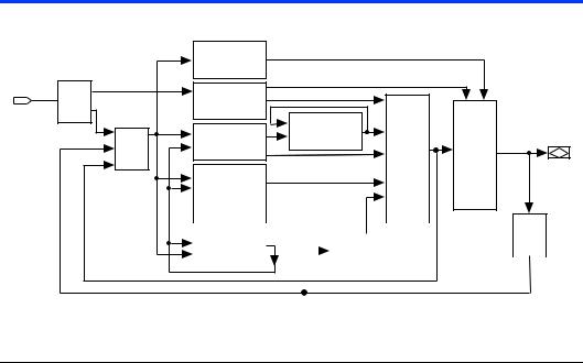
Timing Model |
MAX 7000 device timing can be analyzed with the Altera software, with a |
|
variety of popular industry-standard EDA simulators and timing |
|
analyzers, or with the timing model shown in Figure 12. MAX 7000 |
|
devices have fixed internal delays that enable the designer to determine |
|
the worst-case timing of any design. The Altera software provides timing |
|
simulation, point-to-point delay prediction, and detailed timing analysis |
|
for a device-wide performance evaluation. |
28 |
Altera Corporation |
MAX 7000 Programmable Logic Device Family Data Sheet
Figure 12. MAX 7000 Timing Model
Input
Delay
t I N
|
Internal Output |
|
|
|
|
|
Enable Delay |
|
|
|
|
|
t IOE (1) |
|
|
|
|
|
Global Control |
|
|
|
|
|
Delay |
|
|
Output |
|
|
t GLOB |
Parallel |
Register |
||
|
Logic Array |
Delay |
Delay |
||
PIA |
Expander Delay |
t SU |
t OD1 |
||
Delay |
t PEXP |
||||
Delay |
t H |
t OD2 (2) |
|||
t PIA |
t LAD |
|
t PRE |
t OD3 |
|
|
|
t CLR |
t XZ |
||
|
Register |
|
|||
|
|
t RD |
t Z X1 |
||
|
Control Delay |
|
|||
|
|
t COMB |
t Z X2 (2) |
||
|
t LAC |
|
|||
|
|
t FSU |
t Z X3 (1) |
||
|
t I C |
|
|||
|
|
t FH |
|
||
|
t EN |
|
|
||
|
|
|
|
|
|
|
|
|
|
|
|
|
I/O |
|
|
|
|
|
|
|
|
||
Shared |
|
|
|
|
Fast |
|
|
Delay |
|
Expander Delay |
|
|
|
|
|
|
t I O |
||
|
|
|
|
Input Delay |
|
|
|||
t SEXP |
|
|
|
|
t F I N (1) |
|
|
|
|
|
|
|
|
|
|
|
|
||
|
|
|
|
|
|
|
|
|
|
Notes:
(1)Only available in MAX 7000E and MAX 7000S devices.
(2)Not available in 44-pin devices.
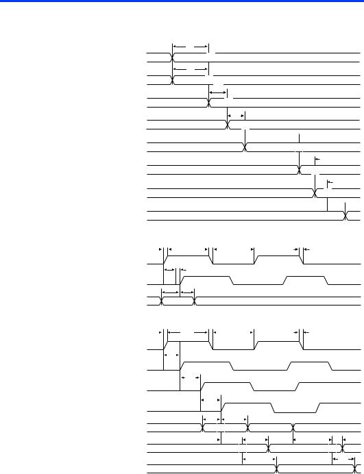
The timing characteristics of any signal path can be derived from the timing model and parameters of a particular device. External timing parameters, which represent pin-to-pin timing delays, can be calculated as the sum of internal parameters. Figure 13 shows the internal timing relationship of internal and external delay parameters.
f For more infomration, see Application Note 94 (Understanding MAX 7000 Timing).
Altera Corporation |
29 |
MAX 7000 Programmable Logic Device Family Data Sheet
Figure 13. Switching Waveforms
tR & tF < 3 ns.
Inputs are driven at 3 V for a logic high and 0 V for a logic low. All timing characteristics are measured at 1.5 V.
Combinatorial Mode
tIN
Input Pin
tIO
I/O Pin
tPIA
PIA Delay
tSEXP
Shared Expander
Delay

 tLAC , tLAD

Logic Array Input
tPEXP 

Parallel Expander Delay
tCOMB 
Logic Array Output

 tOD
tOD 

Output Pin
Global Clock Mode
tR |
|
|
|
tCH |
|
|
|
tCL |
|
tF |
|
|
|
|
|
||||||
Global |
|
|
|
|
|
|
|
|
||
Clock Pin |
|
|
|
|
|
|
|
|
||
tIN
Global Clock tGLOB
at Register
tSU tH
Data or Enable (Logic Array Output)
Array Clock Mode
tR |
|
|
|
tACH |
|
|
|
tACL |
|
|
|
|
|
|
|
|
|
tF |
|
|
|
|
|||||||
|
|
|
|
|
|
|
|
|
|
|
|||||||||||||||||||
Input or I/O Pin |
tIN |
|
|
|
|
|
|
|
|
|
|
|
|
|
|
|
|
|
|
|
|
|
|||||||
|
|
|
|
|
|
|
|
|
|
|
|
|
|
|
|
|
|
|
|
|
|
|
|||||||
|
|
|
tIO |
|
|
|
|
|
|
|
|
|
|
|
|
|
|
|
|
|
|
|
|
||||||
Clock into PIA |
|
|
|
|
|
|
|
|
|
|
|
|
|
|
|
|
|
|
|
|
|
|
|
|
|
|
|
||
Clock into |
|
tPIA |
|
|
|
|
|
|
|
|
|
|
|
|
|
|
|
|
|
|
|
|
|||||||
Logic Array |
|
|
|
|
|
|
|
|
|
|
|
|
|
|
|
|
|
|
|
|
|
|
|
|
|
|
|
||
Clock at |
|
|
|
|
tIC |
|
|
|
|
|
|
|
|
|
|
|
|
|
|
|
|
|
|
|
|
|
|||
|
|
|
|
|
|
|
|
|
|
|
|
|
|
|
|
|
|
|
|
|
|
|
|
|
|||||
Register |
|
|
|
|
|
|
|
|
|
|
|
|
|
|
|
|
|
|
|
|
|
|
|
|
|
|
|
||
|
|
|
|
|
|
|
tSU |
|
|
|
tH |
|
|
|
|
|
|
|
|
||||||||||
Data from |
|
|
|
|
|
|
|
|
|
|
|
|
|
|
|
|
|
|
|
|
|
|
|
|
|
|
|
||
Logic Array |
|
|
|
|
|
|
|
|
|
|
|
|
|
|
|
|
|
|
|
|
|
|
|
|
|
|
|
||
Register to PIA |
|
tRD |
|
|
|
|
|
|
|
|
|
|
tPIA |
|
|
|
|
|
tCLR , tPRE |
|
|
|
tPIA |
||||||
|
|
|
|
|
|
|
|
|
|
|
|
|
|
|
|
|
|
|
|||||||||||
|
|
|
|
|
|
|
|
|
|
|
|
|
|
|
|
|
|
|
|
|
|
|
|
|
|
|
|||
to Logic Array |
|
|
|
|
|
|
|
|
|
|
|
|
|
|
|
|
tOD |
|
|
|
|
|
|
tOD |
|||||
Register Output |
|
|
|
|
|
|
|
|
|
|
|
|
|
|
|
|
|
|
|
|
|
|
|||||||
|
|
|
|
|
|
|
|
|
|
|
|
|
|
|
|
|
|
|
|
|
|
||||||||
to Pin |
|
|
|
|
|
|
|
|
|
|
|
|
|
|
|
|
|
|
|
|
|
|
|
|
|
|
|
||
30 |
Altera Corporation |
MAX 7000 Programmable Logic Device Family Data Sheet
Tables 19 through 26 show the MAX 7000 and MAX 7000E AC operating conditions.
Table 19. MAX 7000 & MAX 7000E External Timing Parameters |
Note (1) |
|
|
|
|||
|
|
|
|
|
|
|
|
Symbol |
Parameter |
Conditions |
-6 Speed Grade |
-7 Speed Grade |
Unit |
||
|
|
|
|
|
|
|
|
|
|
|
Min |
Max |
Min |
Max |
|
|
|
|
|
|
|
|
|
tPD1 |
Input to non-registered output |
C1 = 35 pF |
|
6.0 |
|
7.5 |
ns |
tPD2 |
I/O input to non-registered output |
C1 = 35 pF |
|
6.0 |
|
7.5 |
ns |
tSU |
Global clock setup time |
|
5.0 |
|
6.0 |
|
ns |
tH |
Global clock hold time |
|
0.0 |
|
0.0 |
|
ns |
tFSU |
Global clock setup time of fast input |
(2) |
2.5 |
|
3.0 |
|
ns |
tFH |
Global clock hold time of fast input |
(2) |
0.5 |
|
0.5 |
|
ns |
tCO1 |
Global clock to output delay |
C1 = 35 pF |
|
4.0 |
|
4.5 |
ns |
tCH |
Global clock high time |
|
2.5 |
|
3.0 |
|
ns |
tCL |
Global clock low time |
|
2.5 |
|
3.0 |
|
ns |
tASU |
Array clock setup time |
|
2.5 |
|
3.0 |
|
ns |
tAH |
Array clock hold time |
|
2.0 |
|
2.0 |
|
ns |
tACO1 |
Array clock to output delay |
C1 = 35 pF |
|
6.5 |
|
7.5 |
ns |
tACH |
Array clock high time |
|
3.0 |
|
3.0 |
|
ns |
tACL |
Array clock low time |
|
3.0 |
|
3.0 |
|
ns |
tCPPW |
Minimum pulse width for clear and |
(3) |
3.0 |
|
3.0 |
|
ns |
|
preset |
|
|
|
|
|
|
|
|
|
|
|
|
|
|
tODH |
Output data hold time after clock |
C1 = 35 pF (4) |
1.0 |
|
1.0 |
|
ns |
tCNT |
Minimum global clock period |
|
|
6.6 |
|
8.0 |
ns |
fCNT |
Maximum internal global clock |
(5) |
151.5 |
|
125.0 |
|
MHz |
|
frequency |
|
|
|
|
|
|
|
|
|
|
|
|
|
|
tACNT |
Minimum array clock period |
|
|
6.6 |
|
8.0 |
ns |
fACNT |
Maximum internal array clock |
(5) |
151.5 |
|
125.0 |
|
MHz |
|
frequency |
|
|
|
|
|
|
|
|
|
|
|
|
|
|
fMAX |
Maximum clock frequency |
(6) |
200 |
|
166.7 |
|
MHz |
Altera Corporation |
31 |

MAX 7000 Programmable Logic Device Family Data Sheet
Table 20. MAX 7000 & MAX 7000E Internal Timing Parameters |
Note (1) |
|
|
|
||||
|
|
|
|
|
|
|
|
|
Symbol |
Parameter |
Conditions |
Speed Grade -6 |
Speed Grade -7 |
Unit |
|||
|
|
|
|
|
|
|
|
|
|
|
|
Min |
|
Max |
Min |
Max |
|
|
|
|
|
|
|
|
|
|
tIN |
Input pad and buffer delay |
|
|
|
0.4 |
|
0.5 |
ns |
tIO |
I/O input pad and buffer delay |
|
|
|
0.4 |
|
0.5 |
ns |
tFIN |
Fast input delay |
(2) |
|
|
0.8 |
|
1.0 |
ns |
tSEXP |
Shared expander delay |
|
|
|
3.5 |
|
4.0 |
ns |
tPEXP |
Parallel expander delay |
|
|
|
0.8 |
|
0.8 |
ns |
tLAD |
Logic array delay |
|
|
|
2.0 |
|
3.0 |
ns |
tLAC |
Logic control array delay |
|
|
|
2.0 |
|
3.0 |
ns |
tIOE |
Internal output enable delay |
(2) |
|
|
|
|
2.0 |
ns |
tOD1 |
Output buffer and pad delay |
C1 = 35 pF |
|
|
2.0 |
|
2.0 |
ns |
|
Slow slew rate = off, VCCIO = 5.0 V |
|
|
|
|
|
|
|
tOD2 |
Output buffer and pad delay |
C1 = 35 pF (7) |
|
|
2.5 |
|
2.5 |
ns |
|
Slow slew rate = off, VCCIO = 3.3 V |
|
|
|
|
|
|
|
tOD3 |
Output buffer and pad delay |
C1 = 35 pF (2) |
|
|
7.0 |
|
7.0 |
ns |
|
Slow slew rate = on, |
|
|
|
|
|
|
|
|
VCCIO = 5.0 V or 3.3 V |
|
|
|
|
|
|
|
tZX1 |
Output buffer enable delay |
C1 = 35 pF |
|
|
4.0 |
|
4.0 |
ns |
|
Slow slew rate = off, VCCIO = 5.0 V |
|
|
|
|
|
|
|
tZX2 |
Output buffer enable delay |
C1 = 35 pF (7) |
|
|
4.5 |
|
4.5 |
ns |
|
Slow slew rate = off, VCCIO = 3.3 V |
|
|
|
|
|
|
|
tZX3 |
Output buffer enable delay |
C1 = 35 pF (2) |
|
|
9.0 |
|
9.0 |
ns |
|
Slow slew rate = on |
|
|
|
|
|
|
|
|
VCCIO = 5.0 V or 3.3 V |
|
|
|
|
|
|
|
tXZ |
Output buffer disable delay |
C1 = 5 pF |
|
|
4.0 |
|
4.0 |
ns |
tSU |
Register setup time |
|
3.0 |
|
|
3.0 |
|
ns |
tH |
Register hold time |
|
1.5 |
|
|
2.0 |
|
ns |
tFSU |
Register setup time of fast input |
(2) |
2.5 |
|
|
3.0 |
|
ns |
tFH |
Register hold time of fast input |
(2) |
0.5 |
|
|
0.5 |
|
ns |
tRD |
Register delay |
|
|
|
0.8 |
|
1.0 |
ns |
tCOMB |
Combinatorial delay |
|
|
|
0.8 |
|
1.0 |
ns |
tIC |
Array clock delay |
|
|
|
2.5 |
|
3.0 |
ns |
tEN |
Register enable time |
|
|
|
2.0 |
|
3.0 |
ns |
tGLOB |
Global control delay |
|
|
|
0.8 |
|
1.0 |
ns |
tPRE |
Register preset time |
|
|
|
2.0 |
|
2.0 |
ns |
tCLR |
Register clear time |
|
|
|
2.0 |
|
2.0 |
ns |
tPIA |
PIA delay |
|
|
|
0.8 |
|
1.0 |
ns |
tLPA |
Low-power adder |
(8) |
|
|
10.0 |
|
10.0 |
ns |
32 |
Altera Corporation |

MAX 7000 Programmable Logic Device Family Data Sheet
Table 21. MAX 7000 & MAX 7000E External Timing Parameters |
Note (1) |
|
|
|
|
||||
|
|
|
|
|
|
|
|
|
|
Symbol |
Parameter |
Conditions |
|
|
|
Speed Grade |
|
Unit |
|
|
|
|
|
|
|
|
|
||
|
|
|
|
MAX 7000E (-10P) |
MAX 7000 (-10) |
|
|||
|
|
|
|
|
|
|
MAX 7000E (-10) |
|
|
|
|
|
|
|
|
|
|
|
|
|
|
|
|
Min |
|
Max |
Min |
Max |
|
|
|
|
|
|
|
|
|
|
|
tPD1 |
Input to non-registered output |
C1 = 35 pF |
|
|
|
10.0 |
|
10.0 |
ns |
tPD2 |
I/O input to non-registered output |
C1 = 35 pF |
|
|
|
10.0 |
|
10.0 |
ns |
tSU |
Global clock setup time |
|
|
7.0 |
|
|
8.0 |
|
ns |
tH |
Global clock hold time |
|
|
0.0 |
|
|
0.0 |
|
ns |
tFSU |
Global clock setup time of fast input |
(2) |
|
3.0 |
|
|
3.0 |
|
ns |
tFH |
Global clock hold time of fast input |
(2) |
|
0.5 |
|
|
0.5 |
|
ns |
tCO1 |
Global clock to output delay |
C1 = 35 pF |
|
|
|
5.0 |
|
5 |
ns |
tCH |
Global clock high time |
|
|
4.0 |
|
|
4.0 |
|
ns |
tCL |
Global clock low time |
|
|
4.0 |
|
|
4.0 |
|
ns |
tASU |
Array clock setup time |
|
|
2.0 |
|
|
3.0 |
|
ns |
tAH |
Array clock hold time |
|
|
3.0 |
|
|
3.0 |
|
ns |
tACO1 |
Array clock to output delay |
C1 = 35 pF |
|
|
|
10.0 |
|
10.0 |
ns |
tACH |
Array clock high time |
|
|
4.0 |
|
|
4.0 |
|
ns |
tACL |
Array clock low time |
|
|
4.0 |
|
|
4.0 |
|
ns |
tCPPW |
Minimum pulse width for clear and |
(3) |
|
4.0 |
|
|
4.0 |
|
ns |
|
preset |
|
|
|
|
|
|
|
|
|
|
|
|
|
|
|
|
|
|
tODH |
Output data hold time after clock |
C1 = 35 pF (4) |
|
1.0 |
|
|
1.0 |
|
ns |
tCNT |
Minimum global clock period |
|
|
|
|
10.0 |
|
10.0 |
ns |
fCNT |
Maximum internal global clock |
(5) |
|
100.0 |
|
|
100.0 |
|
MHz |
|
frequency |
|
|
|
|
|
|
|
|
|
|
|
|
|
|
|
|
|
|
tACNT |
Minimum array clock period |
|
|
|
|
10.0 |
|
10.0 |
ns |
fACNT |
Maximum internal array clock |
(5) |
|
100.0 |
|
|
100.0 |
|
MHz |
|
frequency |
|
|
|
|
|
|
|
|
|
|
|
|
|
|
|
|
|
|
fMAX |
Maximum clock frequency |
(6) |
|
125.0 |
|
|
125.0 |
|
MHz |
Altera Corporation |
33 |

MAX 7000 Programmable Logic Device Family Data Sheet
Table 22. MAX 7000 & MAX 7000E Internal Timing Parameters |
Note (1) |
|
|
|
|
||||
|
|
|
|
|
|
|
|
|
|
Symbol |
Parameter |
Conditions |
|
|
|
Speed Grade |
|
Unit |
|
|
|
|
|
|
|
|
|||
|
|
|
MAX 7000E (-10P) |
MAX 7000 (-10) |
|
||||
|
|
|
|
|
|
|
MAX 7000E (-10) |
|
|
|
|
|
|
|
|
|
|
|
|
|
|
|
|
Min |
|
Max |
Min |
Max |
|
|
|
|
|
|
|
|
|
|
|
tIN |
Input pad and buffer delay |
|
|
|
|
0.5 |
|
1.0 |
ns |
tIO |
I/O input pad and buffer delay |
|
|
|
|
0.5 |
|
1.0 |
ns |
tFIN |
Fast input delay |
(2) |
|
|
|
1.0 |
|
1.0 |
ns |
tSEXP |
Shared expander delay |
|
|
|
|
5.0 |
|
5.0 |
ns |
tPEXP |
Parallel expander delay |
|
|
|
|
0.8 |
|
0.8 |
ns |
tLAD |
Logic array delay |
|
|
|
|
5.0 |
|
5.0 |
ns |
tLAC |
Logic control array delay |
|
|
|
|
5.0 |
|
5.0 |
ns |
tIOE |
Internal output enable delay |
(2) |
|
|
|
2.0 |
|
2.0 |
ns |
tOD1 |
Output buffer and pad delay |
C1 = 35 pF |
|
|
|
1.5 |
|
2.0 |
ns |
|
Slow slew rate = off |
|
|
|
|
|
|
|
|
|
VCCIO = 5.0 V |
|
|
|
|
|
|
|
|
tOD2 |
Output buffer and pad delay |
C1 = 35 pF (7) |
|
|
|
2.0 |
|
2.5 |
ns |
|
Slow slew rate = off |
|
|
|
|
|
|
|
|
|
VCCIO = 3.3 V |
|
|
|
|
|
|
|
|
tOD3 |
Output buffer and pad delay |
C1 = 35 pF (2) |
|
|
|
5.5 |
|
6.0 |
ns |
|
Slow slew rate = on |
|
|
|
|
|
|
|
|
|
VCCIO = 5.0 V or 3.3 V |
|
|
|
|
|
|
|
|
tZX1 |
Output buffer enable delay |
C1 = 35 pF |
|
|
|
5.0 |
|
5.0 |
ns |
|
Slow slew rate = off |
|
|
|
|
|
|
|
|
|
VCCIO = 5.0 V |
|
|
|
|
|
|
|
|
tZX2 |
Output buffer enable delay |
C1 = 35 pF (7) |
|
|
|
5.5 |
|
5.5 |
ns |
|
Slow slew rate = off |
|
|
|
|
|
|
|
|
|
VCCIO = 3.3 V |
|
|
|
|
|
|
|
|
tZX3 |
Output buffer enable delay |
C1 = 35 pF (2) |
|
|
|
9.0 |
|
9.0 |
ns |
|
Slow slew rate = on |
|
|
|
|
|
|
|
|
|
VCCIO = 5.0 V or 3.3 V |
|
|
|
|
|
|
|
|
tXZ |
Output buffer disable delay |
C1 = 5 pF |
|
|
|
5.0 |
|
5.0 |
ns |
tSU |
Register setup time |
|
|
2.0 |
|
|
3.0 |
|
ns |
tH |
Register hold time |
|
|
3.0 |
|
|
3.0 |
|
ns |
tFSU |
Register setup time of fast input |
(2) |
|
3.0 |
|
|
3.0 |
|
ns |
tFH |
Register hold time of fast input |
(2) |
|
0.5 |
|
|
0.5 |
|
ns |
tRD |
Register delay |
|
|
|
|
2.0 |
|
1.0 |
ns |
tCOMB |
Combinatorial delay |
|
|
|
|
2.0 |
|
1.0 |
ns |
tIC |
Array clock delay |
|
|
|
|
5.0 |
|
5.0 |
ns |
tEN |
Register enable time |
|
|
|
|
5.0 |
|
5.0 |
ns |
tGLOB |
Global control delay |
|
|
|
|
1.0 |
|
1.0 |
ns |
tPRE |
Register preset time |
|
|
|
|
3.0 |
|
3.0 |
ns |
tCLR |
Register clear time |
|
|
|
|
3.0 |
|
3.0 |
ns |
tPIA |
PIA delay |
|
|
|
|
1.0 |
|
1.0 |
ns |
tLPA |
Low-power adder |
(8) |
|
|
|
11.0 |
|
11.0 |
ns |
34 |
Altera Corporation |

MAX 7000 Programmable Logic Device Family Data Sheet
Table 23. MAX 7000 & MAX 7000E External Timing Parameters |
Note (1) |
|
|
|
||||
|
|
|
|
|
|
|
|
|
Symbol |
Parameter |
Conditions |
|
|
Speed Grade |
|
Unit |
|
|
|
|
|
|
|
|
||
|
|
|
MAX 7000E (-12P) |
MAX 7000 (-12) |
|
|||
|
|
|
|
|
|
MAX 7000E (-12) |
|
|
|
|
|
|
|
|
|
|
|
|
|
|
|
Min |
Max |
Min |
Max |
|
|
|
|
|
|
|
|
|
|
tPD1 |
Input to non-registered output |
C1 = 35 pF |
|
|
12.0 |
|
12.0 |
ns |
tPD2 |
I/O input to non-registered output |
C1 = 35 pF |
|
|
12.0 |
|
12.0 |
ns |
tSU |
Global clock setup time |
|
|
7.0 |
|
10.0 |
|
ns |
tH |
Global clock hold time |
|
|
0.0 |
|
0.0 |
|
ns |
tFSU |
Global clock setup time of fast input |
(2) |
|
3.0 |
|
3.0 |
|
ns |
tFH |
Global clock hold time of fast input |
(2) |
|
0.0 |
|
0.0 |
|
ns |
tCO1 |
Global clock to output delay |
C1 = 35 pF |
|
|
6.0 |
|
6.0 |
ns |
tCH |
Global clock high time |
|
|
4.0 |
|
4.0 |
|
ns |
tCL |
Global clock low time |
|
|
4.0 |
|
4.0 |
|
ns |
tASU |
Array clock setup time |
|
|
3.0 |
|
4.0 |
|
ns |
tAH |
Array clock hold time |
|
|
4.0 |
|
4.0 |
|
ns |
tACO1 |
Array clock to output delay |
C1 = 35 pF |
|
|
12.0 |
|
12.0 |
ns |
tACH |
Array clock high time |
|
|
5.0 |
|
5.0 |
|
ns |
tACL |
Array clock low time |
|
|
5.0 |
|
5.0 |
|
ns |
tCPPW |
Minimum pulse width for clear and |
(3) |
|
5.0 |
|
5.0 |
|
ns |
|
preset |
|
|
|
|
|
|
|
|
|
|
|
|
|
|
|
|
tODH |
Output data hold time after clock |
C1 = 35 pF (4) |
|
1.0 |
|
1.0 |
|
ns |
tCNT |
Minimum global clock period |
|
|
|
11.0 |
|
11.0 |
ns |
fCNT |
Maximum internal global clock |
(5) |
|
90.9 |
|
90.9 |
|
MHz |
|
frequency |
|
|
|
|
|
|
|
|
|
|
|
|
|
|
|
|
tACNT |
Minimum array clock period |
|
|
|
11.0 |
|
11.0 |
ns |
fACNT |
Maximum internal array clock |
(5) |
|
90.9 |
|
90.9 |
|
MHz |
|
frequency |
|
|
|
|
|
|
|
|
|
|
|
|
|
|
|
|
fMAX |
Maximum clock frequency |
(6) |
|
125.0 |
|
125.0 |
|
MHz |
Altera Corporation |
35 |

MAX 7000 Programmable Logic Device Family Data Sheet
Table 24. MAX 7000 & MAX 7000E Internal Timing Parameters |
Note (1) |
|
|
|
|
||||
|
|
|
|
|
|
|
|
|
|
Symbol |
Parameter |
Conditions |
|
|
|
Speed Grade |
|
Unit |
|
|
|
|
|
|
|
|
|||
|
|
|
MAX 7000E (-12P) |
MAX 7000 (-12) |
|
||||
|
|
|
|
|
|
|
MAX 7000E (-12) |
|
|
|
|
|
|
|
|
|
|
|
|
|
|
|
|
Min |
|
Max |
Min |
Max |
|
|
|
|
|
|
|
|
|
|
|
tIN |
Input pad and buffer delay |
|
|
|
|
1.0 |
|
2.0 |
ns |
tIO |
I/O input pad and buffer delay |
|
|
|
|
1.0 |
|
2.0 |
ns |
tFIN |
Fast input delay |
(2) |
|
|
|
1.0 |
|
1.0 |
ns |
tSEXP |
Shared expander delay |
|
|
|
|
7.0 |
|
7.0 |
ns |
tPEXP |
Parallel expander delay |
|
|
|
|
1.0 |
|
1.0 |
ns |
tLAD |
Logic array delay |
|
|
|
|
7.0 |
|
5.0 |
ns |
tLAC |
Logic control array delay |
|
|
|
|
5.0 |
|
5.0 |
ns |
tIOE |
Internal output enable delay |
(2) |
|
|
|
2.0 |
|
2.0 |
ns |
tOD1 |
Output buffer and pad delay |
C1 = 35 pF |
|
|
|
1.0 |
|
3.0 |
ns |
|
Slow slew rate = off |
|
|
|
|
|
|
|
|
|
VCCIO = 5.0 V |
|
|
|
|
|
|
|
|
tOD2 |
Output buffer and pad delay |
C1 = 35 pF (7) |
|
|
|
2.0 |
|
4.0 |
ns |
|
Slow slew rate = off |
|
|
|
|
|
|
|
|
|
VCCIO = 3.3 V |
|
|
|
|
|
|
|
|
tOD3 |
Output buffer and pad delay |
C1 = 35 pF (2) |
|
|
|
5.0 |
|
7.0 |
ns |
|
Slow slew rate = on |
|
|
|
|
|
|
|
|
|
VCCIO = 5.0 V or 3.3 V |
|
|
|
|
|
|
|
|
tZX1 |
Output buffer enable delay |
C1 = 35 pF |
|
|
|
6.0 |
|
6.0 |
ns |
|
Slow slew rate = off |
|
|
|
|
|
|
|
|
|
VCCIO = 5.0 V |
|
|
|
|
|
|
|
|
tZX2 |
Output buffer enable delay |
C1 = 35 pF (7) |
|
|
|
7.0 |
|
7.0 |
ns |
|
Slow slew rate = off |
|
|
|
|
|
|
|
|
|
VCCIO = 3.3 V |
|
|
|
|
|
|
|
|
tZX3 |
Output buffer enable delay |
C1 = 35 pF (2) |
|
|
|
10.0 |
|
10.0 |
ns |
|
Slow slew rate = on |
|
|
|
|
|
|
|
|
|
VCCIO = 5.0 V or 3.3 V |
|
|
|
|
|
|
|
|
tXZ |
Output buffer disable delay |
C1 = 5 pF |
|
|
|
6.0 |
|
6.0 |
ns |
tSU |
Register setup time |
|
|
1.0 |
|
|
4.0 |
|
ns |
tH |
Register hold time |
|
|
6.0 |
|
|
4.0 |
|
ns |
tFSU |
Register setup time of fast input |
(2) |
|
4.0 |
|
|
2.0 |
|
ns |
tFH |
Register hold time of fast input |
(2) |
|
0.0 |
|
|
2.0 |
|
ns |
tRD |
Register delay |
|
|
|
|
2.0 |
|
1.0 |
ns |
tCOMB |
Combinatorial delay |
|
|
|
|
2.0 |
|
1.0 |
ns |
tIC |
Array clock delay |
|
|
|
|
5.0 |
|
5.0 |
ns |
tEN |
Register enable time |
|
|
|
|
7.0 |
|
5.0 |
ns |
tGLOB |
Global control delay |
|
|
|
|
2.0 |
|
0.0 |
ns |
tPRE |
Register preset time |
|
|
|
|
4.0 |
|
3.0 |
ns |
tCLR |
Register clear time |
|
|
|
|
4.0 |
|
3.0 |
ns |
tPIA |
PIA delay |
|
|
|
|
1.0 |
|
1.0 |
ns |
tLPA |
Low-power adder |
(8) |
|
|
|
12.0 |
|
12.0 |
ns |
36 |
Altera Corporation |

MAX 7000 Programmable Logic Device Family Data Sheet
Table 25. MAX 7000 & MAX 7000E External Timing Parameters |
Note (1) |
|
|
|
|
|
||||||
|
|
|
|
|
|
|
|
|
|
|
|
|
Symbol |
Parameter |
Conditions |
|
|
|
|
Speed Grade |
|
|
|
Unit |
|
|
|
|
|
|
|
|
|
|
|
|
|
|
|
|
|
|
-15 |
|
-15T |
|
-20 |
|
|||
|
|
|
|
|
|
|
|
|
|
|
|
|
|
|
|
Min |
|
Max |
|
Min |
Max |
Min |
|
Max |
|
|
|
|
|
|
|
|
|
|
|
|
|
|
tPD1 |
Input to non-registered output |
C1 = 35 pF |
|
|
15.0 |
|
|
15.0 |
|
|
20.0 |
ns |
tPD2 |
I/O input to non-registered |
C1 = 35 pF |
|
|
15.0 |
|
|
15.0 |
|
|
20.0 |
ns |
|
output |
|
|
|
|
|
|
|
|
|
|
|
|
|
|
|
|
|
|
|
|
|
|
|
|
tSU |
Global clock setup time |
|
11.0 |
|
|
|
11.0 |
|
12.0 |
|
|
ns |
tH |
Global clock hold time |
|
0.0 |
|
|
|
0.0 |
|
0.0 |
|
|
ns |
tFSU |
Global clock setup time of fast |
(2) |
3.0 |
|
|
|
– |
|
5.0 |
|
|
ns |
|
input |
|
|
|
|
|
|
|
|
|
|
|
|
|
|
|
|
|
|
|
|
|
|
|
|
tFH |
Global clock hold time of fast |
(2) |
0.0 |
|
|
|
– |
|
0.0 |
|
|
ns |
|
input |
|
|
|
|
|
|
|
|
|
|
|
tCO1 |
Global clock to output delay |
C1 = 35 pF |
|
|
8.0 |
|
|
8.0 |
|
|
12.0 |
ns |
tCH |
Global clock high time |
|
5.0 |
|
|
|
6.0 |
|
6.0 |
|
|
ns |
tCL |
Global clock low time |
|
5.0 |
|
|
|
6.0 |
|
6.0 |
|
|
ns |
tASU |
Array clock setup time |
|
4.0 |
|
|
|
4.0 |
|
5.0 |
|
|
ns |
tAH |
Array clock hold time |
|
4.0 |
|
|
|
4.0 |
|
5.0 |
|
|
ns |
tACO1 |
Array clock to output delay |
C1 = 35 pF |
|
|
15.0 |
|
|
15.0 |
|
|
20.0 |
ns |
tACH |
Array clock high time |
|
6.0 |
|
|
|
6.5 |
|
8.0 |
|
|
ns |
tACL |
Array clock low time |
|
6.0 |
|
|
|
6.5 |
|
8.0 |
|
|
ns |
tCPPW |
Minimum pulse width for clear |
(3) |
6.0 |
|
|
|
6.5 |
|
8.0 |
|
|
ns |
|
and preset |
|
|
|
|
|
|
|
|
|
|
|
|
|
|
|
|
|
|
|
|
|
|
|
|
tODH |
Output data hold time after |
C1 = 35 pF (4) |
1.0 |
|
|
|
1.0 |
|
1.0 |
|
|
ns |
|
clock |
|
|
|
|
|
|
|
|
|
|
|
|
|
|
|
|
|
|
|
|
|
|
|
|
tCNT |
Minimum global clock period |
|
|
|
13.0 |
|
|
13.0 |
|
|
16.0 |
ns |
fCNT |
Maximum internal global clock |
(5) |
76.9 |
|
|
|
76.9 |
|
62.5 |
|
|
MHz |
|
frequency |
|
|
|
|
|
|
|
|
|
|
|
tACNT |
Minimum array clock period |
|
|
|
13.0 |
|
|
13.0 |
|
|
16.0 |
ns |
fACNT |
Maximum internal array clock |
(5) |
76.9 |
|
|
|
76.9 |
|
62.5 |
|
|
MHz |
|
frequency |
|
|
|
|
|
|
|
|
|
|
|
|
|
|
|
|
|
|
|
|
|
|
|
|
fMAX |
Maximum clock frequency |
(6) |
100 |
|
|
|
83.3 |
|
83.3 |
|
|
MHz |
Altera Corporation |
37 |

MAX 7000 Programmable Logic Device Family Data Sheet
Table 26. MAX 7000 & MAX 7000E Internal Timing Parameters |
Note (1) |
|
|
|
|
|
|||||
|
|
|
|
|
|
|
|
|
|
|
|
Symbol |
Parameter |
Conditions |
|
|
|
Speed Grade |
|
|
|
Unit |
|
|
|
|
|
|
|
|
|
|
|
||
|
|
|
-15 |
-15T |
|
-20 |
|
||||
|
|
|
|
|
|
|
|
|
|
|
|
|
|
|
Min |
|
Max |
Min |
Max |
Min |
|
Max |
|
|
|
|
|
|
|
|
|
|
|
|
|
tIN |
Input pad and buffer delay |
|
|
|
2.0 |
|
2.0 |
|
|
3.0 |
ns |
tIO |
I/O input pad and buffer delay |
|
|
|
2.0 |
|
2.0 |
|
|
3.0 |
ns |
tFIN |
Fast input delay |
(2) |
|
|
2.0 |
|
– |
|
|
4.0 |
ns |
tSEXP |
Shared expander delay |
|
|
|
8.0 |
|
10.0 |
|
|
9.0 |
ns |
tPEXP |
Parallel expander delay |
|
|
|
1.0 |
|
1.0 |
|
|
2.0 |
ns |
tLAD |
Logic array delay |
|
|
|
6.0 |
|
6.0 |
|
|
8.0 |
ns |
tLAC |
Logic control array delay |
|
|
|
6.0 |
|
6.0 |
|
|
8.0 |
ns |
tIOE |
Internal output enable delay |
(2) |
|
|
3.0 |
|
– |
|
|
4.0 |
ns |
tOD1 |
Output buffer and pad delay |
C1 = 35 pF |
|
|
4.0 |
|
4.0 |
|
|
5.0 |
ns |
|
Slow slew rate = off |
|
|
|
|
|
|
|
|
|
|
|
VCCIO = 5.0 V |
|
|
|
|
|
|
|
|
|
|
tOD2 |
Output buffer and pad delay |
C1 = 35 pF (7) |
|
|
5.0 |
|
– |
|
|
6.0 |
ns |
|
Slow slew rate = off |
|
|
|
|
|
|
|
|
|
|
|
VCCIO = 3.3 V |
|
|
|
|
|
|
|
|
|
|
tOD3 |
Output buffer and pad delay |
C1 = 35 pF (2) |
|
|
8.0 |
|
– |
|
|
9.0 |
ns |
|
Slow slew rate = on |
|
|
|
|
|
|
|
|
|
|
|
VCCIO = 5.0 V or 3.3 V |
|
|
|
|
|
|
|
|
|
|
tZX1 |
Output buffer enable delay |
C1 = 35 pF |
|
|
6.0 |
|
6.0 |
|
|
10.0 |
ns |
|
Slow slew rate = off |
|
|
|
|
|
|
|
|
|
|
|
VCCIO = 5.0 V |
|
|
|
|
|
|
|
|
|
|
tZX2 |
Output buffer enable delay |
C1 = 35 pF (7) |
|
|
7.0 |
|
– |
|
|
11.0 |
ns |
|
Slow slew rate = off |
|
|
|
|
|
|
|
|
|
|
|
VCCIO = 3.3 V |
|
|
|
|
|
|
|
|
|
|
tZX3 |
Output buffer enable delay |
C1 = 35 pF (2) |
|
|
10.0 |
|
– |
|
|
14.0 |
ns |
|
Slow slew rate = on |
|
|
|
|
|
|
|
|
|
|
|
VCCIO = 5.0 V or 3.3 V |
|
|
|
|
|
|
|
|
|
|
tXZ |
Output buffer disable delay |
C1 = 5 pF |
|
|
6.0 |
|
6.0 |
|
|
10.0 |
ns |
tSU |
Register setup time |
|
4.0 |
|
|
4.0 |
|
4.0 |
|
|
ns |
tH |
Register hold time |
|
4.0 |
|
|
4.0 |
|
5.0 |
|
|
ns |
tFSU |
Register setup time of fast input |
(2) |
2.0 |
|
|
– |
|
4.0 |
|
|
ns |
tFH |
Register hold time of fast input |
(2) |
2.0 |
|
|
– |
|
3.0 |
|
|
ns |
tRD |
Register delay |
|
|
|
1.0 |
|
1.0 |
|
|
1.0 |
ns |
tCOMB |
Combinatorial delay |
|
|
|
1.0 |
|
1.0 |
|
|
1.0 |
ns |
tIC |
Array clock delay |
|
|
|
6.0 |
|
6.0 |
|
|
8.0 |
ns |
tEN |
Register enable time |
|
|
|
6.0 |
|
6.0 |
|
|
8.0 |
ns |
tGLOB |
Global control delay |
|
|
|
1.0 |
|
1.0 |
|
|
3.0 |
ns |
tPRE |
Register preset time |
|
|
|
4.0 |
|
4.0 |
|
|
4.0 |
ns |
tCLR |
Register clear time |
|
|
|
4.0 |
|
4.0 |
|
|
4.0 |
ns |
tPIA |
PIA delay |
|
|
|
2.0 |
|
2.0 |
|
|
3.0 |
ns |
tLPA |
Low-power adder |
(8) |
|
|
13.0 |
|
15.0 |
|
|
15.0 |
ns |
38 |
Altera Corporation |

MAX 7000 Programmable Logic Device Family Data Sheet
Notes to tables:
(1)These values are specified under the recommended operating conditions shown in Table 14. See Figure 13 for more information on switching waveforms.
(2)This parameter applies to MAX 7000E devices only.
(3)This minimum pulse width for preset and clear applies for both global clear and array controls. The tLPA parameter must be added to this minimum width if the clear or reset signal incorporates the tLAD parameter into the signal path.
(4)This parameter is a guideline that is sample-tested only and is based on extensive device characterization. This parameter applies for both global and array clocking.
(5)These parameters are measured with a 16-bit loadable, enabled, up/down counter programmed into each LAB.
(6)The fMAX values represent the highest frequency for pipelined data.
(7)Operating conditions: VCCIO = 3.3 V ± 10% for commercial and industrial use.
(8)The tLPA parameter must be added to the tLAD, tLAC, tIC, tEN, tSEXP, tACL, and tCPPW parameters for macrocells running in the low-power mode.
Tables 27 and 28 show the EPM7032S AC operating conditions.
Table 27. EPM7032S External Timing Parameters (Part 1 of 2) |
Note (1) |
|
|
|
|
|
|
||||||
|
|
|
|
|
|
|
|
|
|
|
|
|
|
Symbol |
Parameter |
Conditions |
|
|
|
|
Speed Grade |
|
|
|
Unit |
||
|
|
|
|
|
|
|
|
|
|
|
|
|
|
|
|
|
-5 |
|
-6 |
-7 |
|
-10 |
|
||||
|
|
|
|
|
|
|
|
|
|
|
|
|
|
|
|
|
Min |
Max |
|
Min |
Max |
Min |
|
Max |
Min |
Max |
|
|
|
|
|
|
|
|
|
|
|
|
|
|
|
tPD1 |
Input to non-registered output |
C1 = 35 pF |
|
5.0 |
|
|
6.0 |
|
|
7.5 |
|
10.0 |
ns |
tPD2 |
I/O input to non-registered |
C1 = 35 pF |
|
5.0 |
|
|
6.0 |
|
|
7.5 |
|
10.0 |
ns |
|
output |
|
|
|
|
|
|
|
|
|
|
|
|
|
|
|
|
|
|
|
|
|
|
|
|
|
|
tSU |
Global clock setup time |
|
2.9 |
|
|
4.0 |
|
5.0 |
|
|
7.0 |
|
ns |
tH |
Global clock hold time |
|
0.0 |
|
|
0.0 |
|
0.0 |
|
|
0.0 |
|
ns |
tFSU |
Global clock setup time of fast |
|
2.5 |
|
|
2.5 |
|
2.5 |
|
|
3.0 |
|
ns |
|
input |
|
|
|
|
|
|
|
|
|
|
|
|
|
|
|
|
|
|
|
|
|
|
|
|
|
|
tFH |
Global clock hold time of fast |
|
0.0 |
|
|
0.0 |
|
0.0 |
|
|
0.5 |
|
ns |
|
input |
|
|
|
|
|
|
|
|
|
|
|
|
|
|
|
|
|
|
|
|
|
|
|
|
|
|
tCO1 |
Global clock to output delay |
C1 = 35 pF |
|
3.2 |
|
|
3.5 |
|
|
4.3 |
|
5.0 |
ns |
tCH |
Global clock high time |
|
2.0 |
|
|
2.5 |
|
3.0 |
|
|
4.0 |
|
ns |
tCL |
Global clock low time |
|
2.0 |
|
|
2.5 |
|
3.0 |
|
|
4.0 |
|
ns |
tASU |
Array clock setup time |
|
0.7 |
|
|
0.9 |
|
1.1 |
|
|
2.0 |
|
ns |
tAH |
Array clock hold time |
|
1.8 |
|
|
2.1 |
|
2.7 |
|
|
3.0 |
|
ns |
tACO1 |
Array clock to output delay |
C1 = 35 pF |
|
5.4 |
|
|
6.6 |
|
|
8.2 |
|
10.0 |
ns |
tACH |
Array clock high time |
|
2.5 |
|
|
2.5 |
|
3.0 |
|
|
4.0 |
|
ns |
tACL |
Array clock low time |
|
2.5 |
|
|
2.5 |
|
3.0 |
|
|
4.0 |
|
ns |
tCPPW |
Minimum pulse width for clear |
(2) |
2.5 |
|
|
2.5 |
|
3.0 |
|
|
4.0 |
|
ns |
|
and preset |
|
|
|
|
|
|
|
|
|
|
|
|
tODH |
Output data hold time after |
C1 = 35 pF (3) |
1.0 |
|
|
1.0 |
|
1.0 |
|
|
1.0 |
|
ns |
|
clock |
|
|
|
|
|
|
|
|
|
|
|
|
|
|
|
|
|
|
|
|
|
|
|
|
|
|
tCNT |
Minimum global clock period |
|
|
5.7 |
|
|
7.0 |
|
|
8.6 |
|
10.0 |
ns |
fCNT |
Maximum internal global clock |
(4) |
175.4 |
|
|
142.9 |
|
116.3 |
|
|
100.0 |
|
MHz |
|
frequency |
|
|
|
|
|
|
|
|
|
|
|
|
tACNT |
Minimum array clock period |
|
|
5.7 |
|
|
7.0 |
|
|
8.6 |
|
10.0 |
ns |
Altera Corporation |
39 |

MAX 7000 Programmable Logic Device Family Data Sheet
Table 27. EPM7032S External Timing Parameters (Part 2 of 2) |
Note (1) |
|
|
|
|
|
|
|
|
|
|||||||||||
|
|
|
|
|
|
|
|
|
|
|
|
|
|
|
|
|
|
|
|
|
|
Symbol |
Parameter |
|
Conditions |
|
|
|
|
|
|
|
Speed Grade |
|
|
|
|
|
|
Unit |
|||
|
|
|
|
|
|
|
|
|
|
|
|
|
|
|
|
|
|
|
|
|
|
|
|
|
|
|
-5 |
|
|
|
-6 |
-7 |
|
-10 |
|
|
|||||||
|
|
|
|
|
|
|
|
|
|
|
|
|
|
|
|
|
|
|
|
|
|
|
|
|
|
|
Min |
Max |
|
Min |
|
Max |
Min |
|
Max |
|
Min |
|
Max |
|
|
||
|
|
|
|
|
|
|
|
|
|
|
|
|
|
|
|
|
|
|
|
|
|
fACNT |
Maximum internal array clock |
|
(4) |
|
175.4 |
|
|
|
|
142.9 |
|
116.3 |
|
|
100.0 |
|
|
|
MHz |
||
|
frequency |
|
|
|
|
|
|
|
|
|
|
|
|
|
|
|
|
|
|
|
|
|
|
|
|
|
|
|
|
|
|
|
|
|
|
|
|
|
|
|
|
|
|
fMAX |
Maximum clock frequency |
|
(5) |
|
250.0 |
|
|
|
|
200.0 |
|
166.7 |
|
|
125.0 |
|
|
|
MHz |
||
|
|
|
|
|
|
|
|
|
|
|
|
|
|
|
|
|
|
|
|||
Table 28. EPM7032S Internal Timing Parameters |
Note (1) |
|
|
|
|
|
|
|
|
|
|
|
|
||||||||
|
|
|
|
|
|
|
|
|
|
|
|
|
|
|
|
|
|
|
|
|
|
Symbol |
Parameter |
|
Conditions |
|
|
|
|
|
|
|
|
Speed Grade |
|
|
|
|
|
|
Unit |
||
|
|
|
|
|
|
|
|
|
|
|
|
|
|
|
|
|
|
|
|||
|
|
|
|
|
-5 |
|
|
|
|
-6 |
-7 |
|
-10 |
|
|
||||||
|
|
|
|
|
|
|
|
|
|
|
|
|
|
|
|
|
|
|
|
||
|
|
|
|
|
Min |
|
Max |
|
|
Min |
|
Max |
Min |
|
Max |
|
Min |
|
Max |
|
|
|
|
|
|
|
|
|
|
|
|
|
|
|
|
|
|
|
|
|
|
|
|
tIN |
Input pad and buffer delay |
|
|
|
|
|
0.2 |
|
|
|
|
0.2 |
|
|
0.3 |
|
|
|
0.5 |
|
ns |
tIO |
I/O input pad and buffer delay |
|
|
|
|
|
0.2 |
|
|
|
|
0.2 |
|
|
0.3 |
|
|
|
0.5 |
|
ns |
tFIN |
Fast input delay |
|
|
|
|
|
2.2 |
|
|
|
|
2.1 |
|
|
2.5 |
|
|
|
1.0 |
|
ns |
tSEXP |
Shared expander delay |
|
|
|
|
|
3.1 |
|
|
|
|
3.8 |
|
|
4.6 |
|
|
|
5.0 |
|
ns |
tPEXP |
Parallel expander delay |
|
|
|
|
|
0.9 |
|
|
|
|
1.1 |
|
|
1.4 |
|
|
|
0.8 |
|
ns |
tLAD |
Logic array delay |
|
|
|
|
|
2.6 |
|
|
|
|
3.3 |
|
|
4.0 |
|
|
|
5.0 |
|
ns |
tLAC |
Logic control array delay |
|
|
|
|
|
2.5 |
|
|
|
|
3.3 |
|
|
4.0 |
|
|
|
5.0 |
|
ns |
tIOE |
Internal output enable delay |
|
|
|
|
|
0.7 |
|
|
|
|
0.8 |
|
|
1.0 |
|
|
|
2.0 |
|
ns |
tOD1 |
Output buffer and pad delay |
C1 = 35 pF |
|
|
|
0.2 |
|
|
|
|
0.3 |
|
|
0.4 |
|
|
|
1.5 |
|
ns |
|
tOD2 |
Output buffer and pad delay |
C1 = 35 pF (6) |
|
|
|
0.7 |
|
|
|
|
0.8 |
|
|
0.9 |
|
|
|
2.0 |
|
ns |
|
tOD3 |
Output buffer and pad delay |
C1 = 35 pF |
|
|
|
5.2 |
|
|
|
|
5.3 |
|
|
5.4 |
|
|
|
5.5 |
|
ns |
|
tZX1 |
Output buffer enable delay |
C1 = 35 pF |
|
|
|
4.0 |
|
|
|
|
4.0 |
|
|
4.0 |
|
|
|
5.0 |
|
ns |
|
tZX2 |
Output buffer enable delay |
C1 = 35 pF (6) |
|
|
|
4.5 |
|
|
|
|
4.5 |
|
|
4.5 |
|
|
|
5.5 |
|
ns |
|
tZX3 |
Output buffer enable delay |
C1 = 35 pF |
|
|
|
9.0 |
|
|
|
|
9.0 |
|
|
9.0 |
|
|
|
9.0 |
|
ns |
|
tXZ |
Output buffer disable delay |
C1 = 5 pF |
|
|
|
4.0 |
|
|
|
|
4.0 |
|
|
4.0 |
|
|
|
5.0 |
|
ns |
|
tSU |
Register setup time |
|
|
|
0.8 |
|
|
|
|
1.0 |
|
|
1.3 |
|
|
|
2.0 |
|
|
|
ns |
tH |
Register hold time |
|
|
|
1.7 |
|
|
|
|
2.0 |
|
|
2.5 |
|
|
|
3.0 |
|
|
|
ns |
tFSU |
Register setup time of fast |
|
|
|
1.9 |
|
|
|
|
1.8 |
|
|
1.7 |
|
|
|
3.0 |
|
|
|
ns |
|
input |
|
|
|
|
|
|
|
|
|
|
|
|
|
|
|
|
|
|
|
|
|
|
|
|
|
|
|
|
|
|
|
|
|
|
|
|
|
|
|
|
|
|
tFH |
Register hold time of fast |
|
|
|
0.6 |
|
|
|
|
0.7 |
|
|
0.8 |
|
|
|
0.5 |
|
|
|
ns |
|
input |
|
|
|
|
|
|
|
|
|
|
|
|
|
|
|
|
|
|
|
|
|
|
|
|
|
|
|
|
|
|
|
|
|
|
|
|
|
|
|
|
|
|
tRD |
Register delay |
|
|
|
|
|
1.2 |
|
|
|
|
1.6 |
|
|
1.9 |
|
|
|
2.0 |
|
ns |
tCOMB |
Combinatorial delay |
|
|
|
|
|
0.9 |
|
|
|
|
1.1 |
|
|
1.4 |
|
|
|
2.0 |
|
ns |
tIC |
Array clock delay |
|
|
|
|
|
2.7 |
|
|
|
|
3.4 |
|
|
4.2 |
|
|
|
5.0 |
|
ns |
tEN |
Register enable time |
|
|
|
|
|
2.6 |
|
|
|
|
3.3 |
|
|
4.0 |
|
|
|
5.0 |
|
ns |
tGLOB |
Global control delay |
|
|
|
|
|
1.6 |
|
|
|
|
1.4 |
|
|
1.7 |
|
|
|
1.0 |
|
ns |
tPRE |
Register preset time |
|
|
|
|
|
2.0 |
|
|
|
|
2.4 |
|
|
3.0 |
|
|
|
3.0 |
|
ns |
tCLR |
Register clear time |
|
|
|
|
|
2.0 |
|
|
|
|
2.4 |
|
|
3.0 |
|
|
|
3.0 |
|
ns |
40 |
Altera Corporation |
MAX 7000 Programmable Logic Device Family Data Sheet
Table 28. EPM7032S Internal Timing Parameters |
Note (1) |
|
|
|
|
|
|
|
|
||||
|
|
|
|
|
|
|
|
|
|
|
|
|
|
Symbol |
Parameter |
Conditions |
|
|
|
|
Speed Grade |
|
|
Unit |
|||
|
|
|
|
|
|
|
|
|
|
|
|
|
|
|
|
|
|
-5 |
-6 |
|
-7 |
-10 |
|
||||
|
|
|
|
|
|
|
|
|
|
|
|
|
|
|
|
|
Min |
|
Max |
Min |
Max |
Min |
|
Max |
Min |
Max |
|
|
|
|
|
|
|
|
|
|
|
|
|
|
|
tPIA |
PIA delay |
(7) |
|
|
1.1 |
|
1.1 |
|
|
1.4 |
|
1.0 |
ns |
tLPA |
Low-power adder |
(8) |
|
|
12.0 |
|
10.0 |
|
|
10.0 |
|
11.0 |
ns |
Notes to tables:
(1)These values are specified under the recommended operating conditions shown in Table 14. See Figure 13 for more information on switching waveforms.
(2)This minimum pulse width for preset and clear applies for both global clear and array controls. The tLPA parameter must be added to this minimum width if the clear or reset signal incorporates the tLAD parameter into the signal path.
(3)This parameter is a guideline that is sample-tested only and is based on extensive device characterization. This parameter applies for both global and array clocking.
(4)These parameters are measured with a 16-bit loadable, enabled, up/down counter programmed into each LAB.
(5)The fMAX values represent the highest frequency for pipelined data.
(6)Operating conditions: VCCIO = 3.3 V ± 10% for commercial and industrial use.
(7)For EPM7064S-5, EPM7064S-6, EPM7128S-6, EPM7160S-6, EPM7160S-7, EPM7192S-7, and EPM7256S-7 devices, these values are specified for a PIA fan-out of one LAB (16 macrocells). For each additional LAB fan-out in these devices, add an additional 0.1 ns to the PIA timing value.
(8)The tLPA parameter must be added to the tLAD, tLAC, tIC, tEN, tSEXP, tACL, and tCPPW parameters for macrocells running in the low-power mode.
Tables 29 and 30 show the EPM7064S AC operating conditions.
Table 29. EPM7064S External Timing Parameters (Part 1 of 2) |
Note (1) |
|
|
|
|
|
||||||
|
|
|
|
|
|
|
|
|
|
|
|
|
Symbol |
Parameter |
Conditions |
|
|
|
Speed Grade |
|
|
Unit |
|||
|
|
|
|
|
|
|
|
|
|
|
|
|
|
|
|
|
-5 |
-6 |
-7 |
-10 |
|
||||
|
|
|
|
|
|
|
|
|
|
|
|
|
|
|
|
Min |
|
Max |
Min |
Max |
Min |
Max |
Min |
Max |
|
|
|
|
|
|
|
|
|
|
|
|
|
|
tPD1 |
Input to non-registered output |
C1 = 35 pF |
|
|
5.0 |
|
6.0 |
|
7.5 |
|
10.0 |
ns |
tPD2 |
I/O input to non-registered |
C1 = 35 pF |
|
|
5.0 |
|
6.0 |
|
7.5 |
|
10.0 |
ns |
|
output |
|
|
|
|
|
|
|
|
|
|
|
tSU |
Global clock setup time |
|
2.9 |
|
|
3.6 |
|
6.0 |
|
7.0 |
|
ns |
tH |
Global clock hold time |
|
0.0 |
|
|
0.0 |
|
0.0 |
|
0.0 |
|
ns |
tFSU |
Global clock setup time of fast |
|
2.5 |
|
|
2.5 |
|
3.0 |
|
3.0 |
|
ns |
|
input |
|
|
|
|
|
|
|
|
|
|
|
|
|
|
|
|
|
|
|
|
|
|
|
|
tFH |
Global clock hold time of fast |
|
0.0 |
|
|
0.0 |
|
0.5 |
|
0.5 |
|
ns |
|
input |
|
|
|
|
|
|
|
|
|
|
|
|
|
|
|
|
|
|
|
|
|
|
|
|
tCO1 |
Global clock to output delay |
C1 = 35 pF |
|
|
3.2 |
|
4.0 |
|
4.5 |
|
5.0 |
ns |
tCH |
Global clock high time |
|
2.0 |
|
|
2.5 |
|
3.0 |
|
4.0 |
|
ns |
tCL |
Global clock low time |
|
2.0 |
|
|
2.5 |
|
3.0 |
|
4.0 |
|
ns |
tASU |
Array clock setup time |
|
0.7 |
|
|
0.9 |
|
3.0 |
|
2.0 |
|
ns |
tAH |
Array clock hold time |
|
1.8 |
|
|
2.1 |
|
2.0 |
|
3.0 |
|
ns |
Altera Corporation |
41 |

MAX 7000 Programmable Logic Device Family Data Sheet
Table 29. EPM7064S External Timing Parameters (Part 2 of 2) |
Note (1) |
|
|
|
|
|
|
|
|
||||||||
|
|
|
|
|
|
|
|
|
|
|
|
|
|
|
|
|
|
Symbol |
Parameter |
|
Conditions |
|
|
|
|
Speed Grade |
|
|
|
|
|
Unit |
|||
|
|
|
|
|
|
|
|
|
|
|
|
|
|
|
|
|
|
|
|
|
|
|
-5 |
-6 |
-7 |
|
-10 |
|
|
||||||
|
|
|
|
|
|
|
|
|
|
|
|
|
|
|
|
|
|
|
|
|
|
|
Min |
|
Max |
Min |
Max |
Min |
|
Max |
Min |
|
Max |
|
|
|
|
|
|
|
|
|
|
|
|
|
|
|
|
|
|
|
|
tACO1 |
Array clock to output delay |
|
C1 = 35 pF |
|
|
5.4 |
|
6.7 |
|
|
7.5 |
|
10.0 |
|
ns |
||
tACH |
Array clock high time |
|
|
|
2.5 |
|
|
2.5 |
|
3.0 |
|
|
4.0 |
|
|
|
ns |
tACL |
Array clock low time |
|
|
|
2.5 |
|
|
2.5 |
|
3.0 |
|
|
4.0 |
|
|
|
ns |
tCPPW |
Minimum pulse width for clear |
|
(2) |
|
2.5 |
|
|
2.5 |
|
3.0 |
|
|
4.0 |
|
|
|
ns |
|
and preset |
|
|
|
|
|
|
|
|
|
|
|
|
|
|
|
|
tODH |
Output data hold time after |
|
C1 = 35 pF (3) |
1.0 |
|
|
1.0 |
|
1.0 |
|
|
1.0 |
|
|
|
ns |
|
|
clock |
|
|
|
|
|
|
|
|
|
|
|
|
|
|
|
|
|
|
|
|
|
|
|
|
|
|
|
|
|
|
|
|
|
|
tCNT |
Minimum global clock period |
|
|
|
|
|
5.7 |
|
7.1 |
|
|
8.0 |
|
10.0 |
|
ns |
|
fCNT |
Maximum internal global clock |
|
(4) |
|
175.4 |
|
|
140.8 |
|
125.0 |
|
|
100.0 |
|
|
|
MHz |
|
frequency |
|
|
|
|
|
|
|
|
|
|
|
|
|
|
|
|
|
|
|
|
|
|
|
|
|
|
|
|
|
|
|
|
|
|
tACNT |
Minimum array clock period |
|
|
|
|
|
5.7 |
|
7.1 |
|
|
8.0 |
|
10.0 |
|
ns |
|
fACNT |
Maximum internal array clock |
|
(4) |
|
175.4 |
|
|
140.8 |
|
125.0 |
|
|
100.0 |
|
|
|
MHz |
|
frequency |
|
|
|
|
|
|
|
|
|
|
|
|
|
|
|
|
|
|
|
|
|
|
|
|
|
|
|
|
|
|
|
|
|
|
fMAX |
Maximum clock frequency |
|
(5) |
|
250.0 |
|
|
200.0 |
|
166.7 |
|
|
125.0 |
|
|
|
MHz |
|
|
|
|
|
|
|
|
|
|
|
|
|
|
|
|||
Table 30. EPM7064S Internal Timing Parameters (Part 1 of 2) |
Note (1) |
|
|
|
|
|
|
|
|
||||||||
|
|
|
|
|
|
|
|
|
|
|
|
|
|
|
|
|
|
Symbol |
Parameter |
|
Conditions |
|
|
|
|
|
Speed Grade |
|
|
|
|
|
Unit |
||
|
|
|
|
|
|
|
|
|
|
|
|
|
|
|
|||
|
|
|
|
|
-5 |
|
-6 |
-7 |
-10 |
|
|
||||||
|
|
|
|
|
|
|
|
|
|
|
|
|
|
|
|
|
|
|
|
|
|
|
Min |
|
Max |
Min |
Max |
Min |
|
Max |
Min |
|
Max |
|
|
|
|
|
|
|
|
|
|
|
|
|
|
|
|
|
|
|
|
tIN |
Input pad and buffer delay |
|
|
|
|
|
0.2 |
|
0.2 |
|
|
0.5 |
|
|
0.5 |
|
ns |
tIO |
I/O input pad and buffer delay |
|
|
|
|
|
0.2 |
|
0.2 |
|
|
0.5 |
|
|
0.5 |
|
ns |
tFIN |
Fast input delay |
|
|
|
|
|
2.2 |
|
2.6 |
|
|
1.0 |
|
|
1.0 |
|
ns |
tSEXP |
Shared expander delay |
|
|
|
|
|
3.1 |
|
3.8 |
|
|
4.0 |
|
|
5.0 |
|
ns |
tPEXP |
Parallel expander delay |
|
|
|
|
|
0.9 |
|
1.1 |
|
|
0.8 |
|
|
0.8 |
|
ns |
tLAD |
Logic array delay |
|
|
|
|
|
2.6 |
|
3.2 |
|
|
3.0 |
|
|
5.0 |
|
ns |
tLAC |
Logic control array delay |
|
|
|
|
|
2.5 |
|
3.2 |
|
|
3.0 |
|
|
5.0 |
|
ns |
tIOE |
Internal output enable delay |
|
|
|
|
|
0.7 |
|
0.8 |
|
|
2.0 |
|
|
2.0 |
|
ns |
tOD1 |
Output buffer and pad delay |
C1 = 35 pF |
|
|
|
0.2 |
|
0.3 |
|
|
2.0 |
|
|
1.5 |
|
ns |
|
tOD2 |
Output buffer and pad delay |
C1 = 35 pF (6) |
|
|
|
0.7 |
|
0.8 |
|
|
2.5 |
|
|
2.0 |
|
ns |
|
tOD3 |
Output buffer and pad delay |
C1 = 35 pF |
|
|
|
5.2 |
|
5.3 |
|
|
7.0 |
|
|
5.5 |
|
ns |
|
tZX1 |
Output buffer enable delay |
C1 = 35 pF |
|
|
|
4.0 |
|
4.0 |
|
|
4.0 |
|
|
5.0 |
|
ns |
|
tZX2 |
Output buffer enable delay |
C1 = 35 pF (6) |
|
|
|
4.5 |
|
4.5 |
|
|
4.5 |
|
|
5.5 |
|
ns |
|
tZX3 |
Output buffer enable delay |
C1 = 35 pF |
|
|
|
9.0 |
|
9.0 |
|
|
9.0 |
|
|
9.0 |
|
ns |
|
tXZ |
Output buffer disable delay |
C1 = 5 pF |
|
|
|
4.0 |
|
4.0 |
|
|
4.0 |
|
|
5.0 |
|
ns |
|
tSU |
Register setup time |
|
|
|
0.8 |
|
|
1.0 |
|
3.0 |
|
|
2.0 |
|
|
|
ns |
tH |
Register hold time |
|
|
|
1.7 |
|
|
2.0 |
|
2.0 |
|
|
3.0 |
|
|
|
ns |
42 |
Altera Corporation |

MAX 7000 Programmable Logic Device Family Data Sheet
Table 30. EPM7064S Internal Timing Parameters (Part 2 of 2) |
Note (1) |
|
|
|
|
|
||||||
|
|
|
|
|
|
|
|
|
|
|
|
|
Symbol |
Parameter |
Conditions |
|
|
|
|
Speed Grade |
|
|
Unit |
||
|
|
|
|
|
|
|
|
|
|
|
|
|
|
|
|
|
-5 |
-6 |
-7 |
-10 |
|
||||
|
|
|
|
|
|
|
|
|
|
|
|
|
|
|
|
Min |
|
Max |
Min |
Max |
Min |
Max |
Min |
Max |
|
|
|
|
|
|
|
|
|
|
|
|
|
|
tFSU |
Register setup time of fast |
|
1.9 |
|
|
1.8 |
|
3.0 |
|
3.0 |
|
ns |
|
input |
|
|
|
|
|
|
|
|
|
|
|
|
|
|
|
|
|
|
|
|
|
|
|
|
tFH |
Register hold time of fast |
|
0.6 |
|
|
0.7 |
|
0.5 |
|
0.5 |
|
ns |
|
input |
|
|
|
|
|
|
|
|
|
|
|
|
|
|
|
|
|
|
|
|
|
|
|
|
tRD |
Register delay |
|
|
|
1.2 |
|
1.6 |
|
1.0 |
|
2.0 |
ns |
tCOMB |
Combinatorial delay |
|
|
|
0.9 |
|
1.0 |
|
1.0 |
|
2.0 |
ns |
tIC |
Array clock delay |
|
|
|
2.7 |
|
3.3 |
|
3.0 |
|
5.0 |
ns |
tEN |
Register enable time |
|
|
|
2.6 |
|
3.2 |
|
3.0 |
|
5.0 |
ns |
tGLOB |
Global control delay |
|
|
|
1.6 |
|
1.9 |
|
1.0 |
|
1.0 |
ns |
tPRE |
Register preset time |
|
|
|
2.0 |
|
2.4 |
|
2.0 |
|
3.0 |
ns |
tCLR |
Register clear time |
|
|
|
2.0 |
|
2.4 |
|
2.0 |
|
3.0 |
ns |
tPIA |
PIA delay |
(7) |
|
|
1.1 |
|
1.3 |
|
1.0 |
|
1.0 |
ns |
tLPA |
Low-power adder |
(8) |
|
|
12.0 |
|
11.0 |
|
10.0 |
|
11.0 |
ns |
Notes to tables:
(1)These values are specified under the recommended operating conditions shown in Table 14. See Figure 13 for more information on switching waveforms.
(2)This minimum pulse width for preset and clear applies for both global clear and array controls. The tLPA parameter must be added to this minimum width if the clear or reset signal incorporates the tLAD parameter into the signal path.
(3)This parameter is a guideline that is sample-tested only and is based on extensive device characterization. This parameter applies for both global and array clocking.
(4)These parameters are measured with a 16-bit loadable, enabled, up/down counter programmed into each LAB.
(5)The fMAX values represent the highest frequency for pipelined data.
(6)Operating conditions: VCCIO = 3.3 V ± 10% for commercial and industrial use.
(7)For EPM7064S-5, EPM7064S-6, EPM7128S-6, EPM7160S-6, EPM7160S-7, EPM7192S-7, and EPM7256S-7 devices, these values are specified for a PIA fan-out of one LAB (16 macrocells). For each additional LAB fan-out in these devices, add an additional 0.1 ns to the PIA timing value.
(8)The tLPA parameter must be added to the tLAD, tLAC, tIC, tEN, tSEXP, tACL, and tCPPW parameters for macrocells running in the low-power mode.
Altera Corporation |
43 |

MAX 7000 Programmable Logic Device Family Data Sheet
Tables 31 and 32 show the EPM7128S AC operating conditions.
Table 31. EPM7128S External Timing Parameters |
Note (1) |
|
|
|
|
|
|
|
|||
|
|
|
|
|
|
|
|
|
|
|
|
Symbol |
Parameter |
Conditions |
|
|
Speed Grade |
|
|
Unit |
|||
|
|
|
|
|
|
|
|
|
|
|
|
|
|
|
-6 |
-7 |
-10 |
-15 |
|
||||
|
|
|
|
|
|
|
|
|
|
|
|
|
|
|
Min |
Max |
Min |
Max |
Min |
Max |
Min |
Max |
|
|
|
|
|
|
|
|
|
|
|
|
|
tPD1 |
Input to non-registered output |
C1 = 35 pF |
|
6.0 |
|
7.5 |
|
10.0 |
|
15.0 |
ns |
tPD2 |
I/O input to non-registered |
C1 = 35 pF |
|
6.0 |
|
7.5 |
|
10.0 |
|
15.0 |
ns |
|
output |
|
|
|
|
|
|
|
|
|
|
|
|
|
|
|
|
|
|
|
|
|
|
tSU |
Global clock setup time |
|
3.4 |
|
6.0 |
|
7.0 |
|
11.0 |
|
ns |
tH |
Global clock hold time |
|
0.0 |
|
0.0 |
|
0.0 |
|
0.0 |
|
ns |
tFSU |
Global clock setup time of fast |
|
2.5 |
|
3.0 |
|
3.0 |
|
3.0 |
|
ns |
|
input |
|
|
|
|
|
|
|
|
|
|
|
|
|
|
|
|
|
|
|
|
|
|
tFH |
Global clock hold time of fast |
|
0.0 |
|
0.5 |
|
0.5 |
|
0.0 |
|
ns |
|
input |
|
|
|
|
|
|
|
|
|
|
|
|
|
|
|
|
|
|
|
|
|
|
tCO1 |
Global clock to output delay |
C1 = 35 pF |
|
4.0 |
|
4.5 |
|
5.0 |
|
8.0 |
ns |
tCH |
Global clock high time |
|
3.0 |
|
3.0 |
|
4.0 |
|
5.0 |
|
ns |
tCL |
Global clock low time |
|
3.0 |
|
3.0 |
|
4.0 |
|
5.0 |
|
ns |
tASU |
Array clock setup time |
|
0.9 |
|
3.0 |
|
2.0 |
|
4.0 |
|
ns |
tAH |
Array clock hold time |
|
1.8 |
|
2.0 |
|
5.0 |
|
4.0 |
|
ns |
tACO1 |
Array clock to output delay |
C1 = 35 pF |
|
6.5 |
|
7.5 |
|
10.0 |
|
15.0 |
ns |
tACH |
Array clock high time |
|
3.0 |
|
3.0 |
|
4.0 |
|
6.0 |
|
ns |
tACL |
Array clock low time |
|
3.0 |
|
3.0 |
|
4.0 |
|
6.0 |
|
ns |
tCPPW |
Minimum pulse width for clear |
(2) |
3.0 |
|
3.0 |
|
4.0 |
|
6.0 |
|
ns |
|
and preset |
|
|
|
|
|
|
|
|
|
|
|
|
|
|
|
|
|
|
|
|
|
|
tODH |
Output data hold time after |
C1 = 35 pF (3) |
1.0 |
|
1.0 |
|
1.0 |
|
1.0 |
|
ns |
|
clock |
|
|
|
|
|
|
|
|
|
|
|
|
|
|
|
|
|
|
|
|
|
|
tCNT |
Minimum global clock period |
|
|
6.8 |
|
8.0 |
|
10.0 |
|
13.0 |
ns |
fCNT |
Maximum internal global clock |
(4) |
147.1 |
|
125.0 |
|
100.0 |
|
76.9 |
|
MHz |
|
frequency |
|
|
|
|
|
|
|
|
|
|
|
|
|
|
|
|
|
|
|
|
|
|
tACNT |
Minimum array clock period |
|
|
6.8 |
|
8.0 |
|
10.0 |
|
13.0 |
ns |
fACNT |
Maximum internal array clock |
(4) |
147.1 |
|
125.0 |
|
100.0 |
|
76.9 |
|
MHz |
|
frequency |
|
|
|
|
|
|
|
|
|
|
|
|
|
|
|
|
|
|
|
|
|
|
fMAX |
Maximum clock frequency |
(5) |
166.7 |
|
166.7 |
|
125.0 |
|
100.0 |
|
MHz |
44 |
Altera Corporation |

MAX 7000 Programmable Logic Device Family Data Sheet
Table 32. EPM7128S Internal Timing Parameters |
Note (1) |
|
|
|
|
|
|
|
||||
|
|
|
|
|
|
|
|
|
|
|
|
|
Symbol |
Parameter |
Conditions |
|
|
|
Speed Grade |
|
|
Unit |
|||
|
|
|
|
|
|
|
|
|
|
|
|
|
|
|
|
|
-6 |
-7 |
-10 |
-15 |
|
||||
|
|
|
|
|
|
|
|
|
|
|
|
|
|
|
|
|
Min |
Max |
Min |
Max |
Min |
Max |
Min |
Max |
|
|
|
|
|
|
|
|
|
|
|
|
|
|
tIN |
Input pad and buffer delay |
|
|
|
0.2 |
|
0.5 |
|
0.5 |
|
2.0 |
ns |
tIO |
I/O input pad and buffer delay |
|
|
|
0.2 |
|
0.5 |
|
0.5 |
|
2.0 |
ns |
tFIN |
Fast input delay |
|
|
|
2.6 |
|
1.0 |
|
1.0 |
|
2.0 |
ns |
tSEXP |
Shared expander delay |
|
|
|
3.7 |
|
4.0 |
|
5.0 |
|
8.0 |
ns |
tPEXP |
Parallel expander delay |
|
|
|
1.1 |
|
0.8 |
|
0.8 |
|
1.0 |
ns |
tLAD |
Logic array delay |
|
|
|
3.0 |
|
3.0 |
|
5.0 |
|
6.0 |
ns |
tLAC |
Logic control array delay |
|
|
|
3.0 |
|
3.0 |
|
5.0 |
|
6.0 |
ns |
tIOE |
Internal output enable delay |
|
|
|
0.7 |
|
2.0 |
|
2.0 |
|
3.0 |
ns |
tOD1 |
Output buffer and pad delay |
C1 |
= 35 pF |
|
0.4 |
|
2.0 |
|
1.5 |
|
4.0 |
ns |
tOD2 |
Output buffer and pad delay |
C1 |
= 35 pF (6) |
|
0.9 |
|
2.5 |
|
2.0 |
|
5.0 |
ns |
tOD3 |
Output buffer and pad delay |
C1 |
= 35 pF |
|
5.4 |
|
7.0 |
|
5.5 |
|
8.0 |
ns |
tZX1 |
Output buffer enable delay |
C1 |
= 35 pF |
|
4.0 |
|
4.0 |
|
5.0 |
|
6.0 |
ns |
tZX2 |
Output buffer enable delay |
C1 |
= 35 pF (6) |
|
4.5 |
|
4.5 |
|
5.5 |
|
7.0 |
ns |
tZX3 |
Output buffer enable delay |
C1 |
= 35 pF |
|
9.0 |
|
9.0 |
|
9.0 |
|
10.0 |
ns |
tXZ |
Output buffer disable delay |
C1 |
= 5 pF |
|
4.0 |
|
4.0 |
|
5.0 |
|
6.0 |
ns |
tSU |
Register setup time |
|
|
1.0 |
|
3.0 |
|
2.0 |
|
4.0 |
|
ns |
tH |
Register hold time |
|
|
1.7 |
|
2.0 |
|
5.0 |
|
4.0 |
|
ns |
tFSU |
Register setup time of fast |
|
|
1.9 |
|
3.0 |
|
3.0 |
|
2.0 |
|
ns |
|
input |
|
|
|
|
|
|
|
|
|
|
|
|
|
|
|
|
|
|
|
|
|
|
|
|
tFH |
Register hold time of fast |
|
|
0.6 |
|
0.5 |
|
0.5 |
|
1.0 |
|
ns |
|
input |
|
|
|
|
|
|
|
|
|
|
|
|
|
|
|
|
|
|
|
|
|
|
|
|
tRD |
Register delay |
|
|
|
1.4 |
|
1.0 |
|
2.0 |
|
1.0 |
ns |
tCOMB |
Combinatorial delay |
|
|
|
1.0 |
|
1.0 |
|
2.0 |
|
1.0 |
ns |
tIC |
Array clock delay |
|
|
|
3.1 |
|
3.0 |
|
5.0 |
|
6.0 |
ns |
tEN |
Register enable time |
|
|
|
3.0 |
|
3.0 |
|
5.0 |
|
6.0 |
ns |
tGLOB |
Global control delay |
|
|
|
2.0 |
|
1.0 |
|
1.0 |
|
1.0 |
ns |
tPRE |
Register preset time |
|
|
|
2.4 |
|
2.0 |
|
3.0 |
|
4.0 |
ns |
tCLR |
Register clear time |
|
|
|
2.4 |
|
2.0 |
|
3.0 |
|
4.0 |
ns |
tPIA |
PIA delay |
(7) |
|
|
1.4 |
|
1.0 |
|
1.0 |
|
2.0 |
ns |
tLPA |
Low-power adder |
(8) |
|
|
11.0 |
|
10.0 |
|
11.0 |
|
13.0 |
ns |
Altera Corporation |
45 |

MAX 7000 Programmable Logic Device Family Data Sheet
Notes to tables:
(1)These values are specified under the recommended operating conditions shown in Table 14. See Figure 13 for more information on switching waveforms.
(2)This minimum pulse width for preset and clear applies for both global clear and array controls. The tLPA parameter must be added to this minimum width if the clear or reset signal incorporates the tLAD parameter into the signal path.
(3)This parameter is a guideline that is sample-tested only and is based on extensive device characterization. This parameter applies for both global and array clocking.
(4)These parameters are measured with a 16-bit loadable, enabled, up/down counter programmed into each LAB.
(5)The fMAX values represent the highest frequency for pipelined data.
(6)Operating conditions: VCCIO = 3.3 V ± 10% for commercial and industrial use.
(7)For EPM7064S-5, EPM7064S-6, EPM7128S-6, EPM7160S-6, EPM7160S-7, EPM7192S-7, and EPM7256S-7 devices, these values are specified for a PIA fan-out of one LAB (16 macrocells). For each additional LAB fan-out in these devices, add an additional 0.1 ns to the PIA timing value.
(8)The tLPA parameter must be added to the tLAD, tLAC, tIC, tEN, tSEXP, tACL, and tCPPW parameters for macrocells running in the low-power mode.
Tables 33 and 34 show the EPM7160S AC operating conditions.
Table 33. EPM7160S External Timing Parameters (Part 1 of 2) |
Note (1) |
|
|
|
|
|
|||||
|
|
|
|
|
|
|
|
|
|
|
|
Symbol |
Parameter |
Conditions |
|
|
Speed Grade |
|
|
Unit |
|||
|
|
|
|
|
|
|
|
|
|
|
|
|
|
|
-6 |
-7 |
-10 |
-15 |
|
||||
|
|
|
|
|
|
|
|
|
|
|
|
|
|
|
Min |
Max |
Min |
Max |
Min |
Max |
Min |
Max |
|
|
|
|
|
|
|
|
|
|
|
|
|
tPD1 |
Input to non-registered output |
C1 = 35 pF |
|
6.0 |
|
7.5 |
|
10.0 |
|
15.0 |
ns |
tPD2 |
I/O input to non-registered |
C1 = 35 pF |
|
6.0 |
|
7.5 |
|
10.0 |
|
15.0 |
ns |
|
output |
|
|
|
|
|
|
|
|
|
|
|
|
|
|
|
|
|
|
|
|
|
|
tSU |
Global clock setup time |
|
3.4 |
|
4.2 |
|
7.0 |
|
11.0 |
|
ns |
tH |
Global clock hold time |
|
0.0 |
|
0.0 |
|
0.0 |
|
0.0 |
|
ns |
tFSU |
Global clock setup time of fast |
|
2.5 |
|
3.0 |
|
3.0 |
|
3.0 |
|
ns |
|
input |
|
|
|
|
|
|
|
|
|
|
|
|
|
|
|
|
|
|
|
|
|
|
tFH |
Global clock hold time of fast |
|
0.0 |
|
0.0 |
|
0.5 |
|
0.0 |
|
ns |
|
input |
|
|
|
|
|
|
|
|
|
|
|
|
|
|
|
|
|
|
|
|
|
|
tCO1 |
Global clock to output delay |
C1 = 35 pF |
|
3.9 |
|
4.8 |
|
5 |
|
8 |
ns |
tCH |
Global clock high time |
|
3.0 |
|
3.0 |
|
4.0 |
|
5.0 |
|
ns |
tCL |
Global clock low time |
|
3.0 |
|
3.0 |
|
4.0 |
|
5.0 |
|
ns |
tASU |
Array clock setup time |
|
0.9 |
|
1.1 |
|
2.0 |
|
4.0 |
|
ns |
tAH |
Array clock hold time |
|
1.7 |
|
2.1 |
|
3.0 |
|
4.0 |
|
ns |
tACO1 |
Array clock to output delay |
C1 = 35 pF |
|
6.4 |
|
7.9 |
|
10.0 |
|
15.0 |
ns |
tACH |
Array clock high time |
|
3.0 |
|
3.0 |
|
4.0 |
|
6.0 |
|
ns |
tACL |
Array clock low time |
|
3.0 |
|
3.0 |
|
4.0 |
|
6.0 |
|
ns |
tCPPW |
Minimum pulse width for clear |
(2) |
2.5 |
|
3.0 |
|
4.0 |
|
6.0 |
|
ns |
|
and preset |
|
|
|
|
|
|
|
|
|
|
tODH |
Output data hold time after |
C1 = 35 pF (3) |
1.0 |
|
1.0 |
|
1.0 |
|
1.0 |
|
ns |
|
clock |
|
|
|
|
|
|
|
|
|
|
|
|
|
|
|
|
|
|
|
|
|
|
tCNT |
Minimum global clock period |
|
|
6.7 |
|
8.2 |
|
10.0 |
|
13.0 |
ns |
fCNT |
Maximum internal global clock |
(4) |
149.3 |
|
122.0 |
|
100.0 |
|
76.9 |
|
MHz |
|
frequency |
|
|
|
|
|
|
|
|
|
|
46 |
Altera Corporation |

MAX 7000 Programmable Logic Device Family Data Sheet
Table 33. EPM7160S External Timing Parameters (Part 2 of 2) |
Note (1) |
|
|
|
|
|
|
|
|
|||||||||
|
|
|
|
|
|
|
|
|
|
|
|
|
|
|
|
|
|
|
Symbol |
Parameter |
|
Conditions |
|
|
|
|
|
Speed Grade |
|
|
|
|
|
|
Unit |
||
|
|
|
|
|
|
|
|
|
|
|
|
|
|
|
|
|
|
|
|
|
|
|
|
-6 |
|
-7 |
-10 |
-15 |
|
|
|||||||
|
|
|
|
|
|
|
|
|
|
|
|
|
|
|
|
|
|
|
|
|
|
|
|
Min |
|
Max |
Min |
|
Max |
Min |
Max |
|
Min |
|
Max |
|
|
|
|
|
|
|
|
|
|
|
|
|
|
|
|
|
|
|
|
|
tACNT |
Minimum array clock period |
|
|
|
|
|
6.7 |
|
|
8.2 |
|
10.0 |
|
|
13.0 |
|
ns |
|
fACNT |
Maximum internal array clock |
|
(4) |
|
149.3 |
|
|
122.0 |
|
100.0 |
|
76.9 |
|
|
|
MHz |
||
|
frequency |
|
|
|
|
|
|
|
|
|
|
|
|
|
|
|
|
|
|
|
|
|
|
|
|
|
|
|
|
|
|
|
|
|
|
|
|
fMAX |
Maximum clock frequency |
|
(5) |
|
166.7 |
|
|
166.7 |
|
125.0 |
|
100.0 |
|
|
|
MHz |
||
|
|
|
|
|
|
|
|
|
|
|
|
|
|
|
||||
Table 34. EPM7160S Internal Timing Parameters (Part 1 of 2) |
Note (1) |
|
|
|
|
|
|
|
|
|||||||||
|
|
|
|
|
|
|
|
|
|
|
|
|
|
|
|
|
|
|
Symbol |
Parameter |
|
Conditions |
|
|
|
|
|
|
Speed Grade |
|
|
|
|
|
|
Unit |
|
|
|
|
|
|
|
|
|
|
|
|
|
|
|
|
|
|
||
|
|
|
|
|
-6 |
|
|
-7 |
-10 |
|
-15 |
|
|
|||||
|
|
|
|
|
|
|
|
|
|
|
|
|
|
|
|
|
|
|
|
|
|
|
|
Min |
|
Max |
Min |
|
Max |
Min |
Max |
|
Min |
|
Max |
|
|
|
|
|
|
|
|
|
|
|
|
|
|
|
|
|
|
|
|
|
tIN |
Input pad and buffer delay |
|
|
|
|
|
0.2 |
|
|
0.3 |
|
0.5 |
|
|
|
2.0 |
|
ns |
tIO |
I/O input pad and buffer delay |
|
|
|
|
|
0.2 |
|
|
0.3 |
|
0.5 |
|
|
|
2.0 |
|
ns |
tFIN |
Fast input delay |
|
|
|
|
|
2.6 |
|
|
3.2 |
|
1.0 |
|
|
|
2.0 |
|
ns |
tSEXP |
Shared expander delay |
|
|
|
|
|
3.6 |
|
|
4.3 |
|
5.0 |
|
|
|
8.0 |
|
ns |
tPEXP |
Parallel expander delay |
|
|
|
|
|
1.0 |
|
|
1.3 |
|
0.8 |
|
|
|
1.0 |
|
ns |
tLAD |
Logic array delay |
|
|
|
|
|
2.8 |
|
|
3.4 |
|
5.0 |
|
|
|
6.0 |
|
ns |
tLAC |
Logic control array delay |
|
|
|
|
|
2.8 |
|
|
3.4 |
|
5.0 |
|
|
|
6.0 |
|
ns |
tIOE |
Internal output enable delay |
|
|
|
|
|
0.7 |
|
|
0.9 |
|
2.0 |
|
|
|
3.0 |
|
ns |
tOD1 |
Output buffer and pad delay |
C1 = 35 pF |
|
|
|
0.4 |
|
|
0.5 |
|
1.5 |
|
|
|
4.0 |
|
ns |
|
tOD2 |
Output buffer and pad delay |
C1 = 35 pF (6) |
|
|
|
0.9 |
|
|
1.0 |
|
2.0 |
|
|
|
5.0 |
|
ns |
|
tOD3 |
Output buffer and pad delay |
C1 = 35 pF |
|
|
|
5.4 |
|
|
5.5 |
|
5.5 |
|
|
|
8.0 |
|
ns |
|
tZX1 |
Output buffer enable delay |
C1 = 35 pF |
|
|
|
4.0 |
|
|
4.0 |
|
5.0 |
|
|
|
6.0 |
|
ns |
|
tZX2 |
Output buffer enable delay |
C1 = 35 pF (6) |
|
|
|
4.5 |
|
|
4.5 |
|
5.5 |
|
|
|
7.0 |
|
ns |
|
tZX3 |
Output buffer enable delay |
C1 = 35 pF |
|
|
|
9.0 |
|
|
9.0 |
|
9.0 |
|
|
|
10.0 |
|
ns |
|
tXZ |
Output buffer disable delay |
C1 = 5 pF |
|
|
|
4.0 |
|
|
4.0 |
|
5.0 |
|
|
|
6.0 |
|
ns |
|
tSU |
Register setup time |
|
|
|
1.0 |
|
|
1.2 |
|
|
2.0 |
|
|
4.0 |
|
|
|
ns |
tH |
Register hold time |
|
|
|
1.6 |
|
|
2.0 |
|
|
3.0 |
|
|
4.0 |
|
|
|
ns |
tFSU |
Register setup time of fast |
|
|
|
1.9 |
|
|
2.2 |
|
|
3.0 |
|
|
2.0 |
|
|
|
ns |
|
input |
|
|
|
|
|
|
|
|
|
|
|
|
|
|
|
|
|
|
|
|
|
|
|
|
|
|
|
|
|
|
|
|
|
|
|
|
tFH |
Register hold time of fast |
|
|
|
0.6 |
|
|
0.8 |
|
|
0.5 |
|
|
1.0 |
|
|
|
ns |
|
input |
|
|
|
|
|
|
|
|
|
|
|
|
|
|
|
|
|
|
|
|
|
|
|
|
|
|
|
|
|
|
|
|
|
|
|
|
tRD |
Register delay |
|
|
|
|
|
1.3 |
|
|
1.6 |
|
2.0 |
|
|
|
1.0 |
|
ns |
tCOMB |
Combinatorial delay |
|
|
|
|
|
1.0 |
|
|
1.3 |
|
2.0 |
|
|
|
1.0 |
|
ns |
tIC |
Array clock delay |
|
|
|
|
|
2.9 |
|
|
3.5 |
|
5.0 |
|
|
|
6.0 |
|
ns |
tEN |
Register enable time |
|
|
|
|
|
2.8 |
|
|
3.4 |
|
5.0 |
|
|
|
6.0 |
|
ns |
tGLOB |
Global control delay |
|
|
|
|
|
2.0 |
|
|
2.4 |
|
1.0 |
|
|
|
1.0 |
|
ns |
tPRE |
Register preset time |
|
|
|
|
|
2.4 |
|
|
3.0 |
|
3.0 |
|
|
|
4.0 |
|
ns |
Altera Corporation |
47 |

MAX 7000 Programmable Logic Device Family Data Sheet
Table 34. EPM7160S Internal Timing Parameters (Part 2 of 2) |
Note (1) |
|
|
|
|
|
||||||
|
|
|
|
|
|
|
|
|
|
|
|
|
Symbol |
Parameter |
Conditions |
|
|
|
|
Speed Grade |
|
|
Unit |
||
|
|
|
|
|
|
|
|
|
|
|
|
|
|
|
|
|
-6 |
-7 |
-10 |
-15 |
|
||||
|
|
|
|
|
|
|
|
|
|
|
|
|
|
|
|
Min |
|
Max |
Min |
Max |
Min |
Max |
Min |
Max |
|
|
|
|
|
|
|
|
|
|
|
|
|
|
tCLR |
Register clear time |
|
|
|
2.4 |
|
3.0 |
|
3.0 |
|
4.0 |
ns |
tPIA |
PIA delay |
(7) |
|
|
1.6 |
|
2.0 |
|
1.0 |
|
2.0 |
ns |
tLPA |
Low-power adder |
(8) |
|
|
11.0 |
|
10.0 |
|
11.0 |
|
13.0 |
ns |
Notes to tables:
(1)These values are specified under the recommended operating conditions shown in Table 14. See Figure 13 for more information on switching waveforms.
(2)This minimum pulse width for preset and clear applies for both global clear and array controls. The tLPA parameter must be added to this minimum width if the clear or reset signal incorporates the tLAD parameter into the signal path.
(3)This parameter is a guideline that is sample-tested only and is based on extensive device characterization. This parameter applies for both global and array clocking.
(4)These parameters are measured with a 16-bit loadable, enabled, up/down counter programmed into each LAB.
(5)The fMAX values represent the highest frequency for pipelined data.
(6)Operating conditions: VCCIO = 3.3 V ± 10% for commercial and industrial use.
(7)For EPM7064S-5, EPM7064S-6, EPM7128S-6, EPM7160S-6, EPM7160S-7, EPM7192S-7, and EPM7256S-7 devices, these values are specified for a PIA fan-out of one LAB (16 macrocells). For each additional LAB fan-out in these devices, add an additional 0.1 ns to the PIA timing value.
(8)The tLPA parameter must be added to the tLAD, tLAC, tIC, tEN, tSEXP, tACL, and tCPPW parameters for macrocells running in the low-power mode.
Tables 35 and 36 show the EPM7192S AC operating conditions.
Table 35. EPM7192S External Timing Parameters (Part 1 of 2) |
Note (1) |
|
|
|
|
|
|
|||||
|
|
|
|
|
|
|
|
|
|
|
|
|
Symbol |
Parameter |
Conditions |
|
|
|
Speed Grade |
|
|
Unit |
|||
|
|
|
|
|
|
|
|
|
|
|
|
|
|
|
|
-7 |
|
|
-10 |
|
-15 |
|
|||
|
|
|
|
|
|
|
|
|
|
|
|
|
|
|
|
Min |
|
Max |
Min |
|
Max |
Min |
|
Max |
|
|
|
|
|
|
|
|
|
|
|
|
|
|
tPD1 |
Input to non-registered output |
C1 = 35 pF |
|
|
7.5 |
|
|
10.0 |
|
|
15.0 |
ns |
tPD2 |
I/O input to non-registered |
C1 = 35 pF |
|
|
7.5 |
|
|
10.0 |
|
|
15.0 |
ns |
|
output |
|
|
|
|
|
|
|
|
|
|
|
|
|
|
|
|
|
|
|
|
|
|
|
|
tSU |
Global clock setup time |
|
4.1 |
|
|
7.0 |
|
|
11.0 |
|
|
ns |
tH |
Global clock hold time |
|
0.0 |
|
|
0.0 |
|
|
0.0 |
|
|
ns |
tFSU |
Global clock setup time of fast |
|
3.0 |
|
|
3.0 |
|
|
3.0 |
|
|
ns |
|
input |
|
|
|
|
|
|
|
|
|
|
|
|
|
|
|
|
|
|
|
|
|
|
|
|
tFH |
Global clock hold time of fast |
|
0.0 |
|
|
0.5 |
|
|
0.0 |
|
|
ns |
|
input |
|
|
|
|
|
|
|
|
|
|
|
|
|
|
|
|
|
|
|
|
|
|
|
|
tCO1 |
Global clock to output delay |
C1 = 35 pF |
|
|
4.7 |
|
|
5.0 |
|
|
8.0 |
ns |
tCH |
Global clock high time |
|
3.0 |
|
|
4.0 |
|
|
5.0 |
|
|
ns |
tCL |
Global clock low time |
|
3.0 |
|
|
4.0 |
|
|
5.0 |
|
|
ns |
tASU |
Array clock setup time |
|
1.0 |
|
|
2.0 |
|
|
4.0 |
|
|
ns |
48 |
Altera Corporation |

MAX 7000 Programmable Logic Device Family Data Sheet
Table 35. EPM7192S External Timing Parameters (Part 2 of 2) |
|
Note (1) |
|
|
|
|
|
|
|
|
|
|||||||||
|
|
|
|
|
|
|
|
|
|
|
|
|
|
|
|
|
|
|
|
|
Symbol |
Parameter |
|
Conditions |
|
|
|
|
|
|
Speed Grade |
|
|
|
|
|
Unit |
||||
|
|
|
|
|
|
|
|
|
|
|
|
|
|
|
|
|
|
|
|
|
|
|
|
|
-7 |
|
|
|
-10 |
|
|
-15 |
|
|
|||||||
|
|
|
|
|
|
|
|
|
|
|
|
|
|
|
|
|
|
|
|
|
|
|
|
|
Min |
|
Max |
|
|
Min |
|
Max |
|
|
Min |
|
Max |
|
|
||
|
|
|
|
|
|
|
|
|
|
|
|
|
|
|
|
|
|
|
|
|
tAH |
Array clock hold time |
|
|
1.8 |
|
|
|
|
3.0 |
|
|
|
4.0 |
|
|
|
ns |
|||
tACO1 |
Array clock to output delay |
|
C1 = 35 pF |
|
|
|
7.8 |
|
|
|
10.0 |
|
|
|
15.0 |
|
ns |
|||
tACH |
Array clock high time |
|
|
3.0 |
|
|
|
|
4.0 |
|
|
|
6.0 |
|
|
|
ns |
|||
tACL |
Array clock low time |
|
|
3.0 |
|
|
|
|
4.0 |
|
|
|
6.0 |
|
|
|
ns |
|||
tCPPW |
Minimum pulse width for clear |
|
(2) |
3.0 |
|
|
|
|
4.0 |
|
|
|
6.0 |
|
|
|
ns |
|||
|
and preset |
|
|
|
|
|
|
|
|
|
|
|
|
|
|
|
|
|
|
|
|
|
|
|
|
|
|
|
|
|
|
|
|
|
|
|
|
|
|
|
|
tODH |
Output data hold time after |
|
C1 = 35 pF (3) |
1.0 |
|
|
|
|
1.0 |
|
|
|
1.0 |
|
|
|
ns |
|||
|
clock |
|
|
|
|
|
|
|
|
|
|
|
|
|
|
|
|
|
|
|
|
|
|
|
|
|
|
|
|
|
|
|
|
|
|
|
|
|
|
|
|
tCNT |
Minimum global clock period |
|
|
|
|
|
8.0 |
|
|
|
10.0 |
|
|
|
13.0 |
|
ns |
|||
fCNT |
Maximum internal global clock |
|
(4) |
125.0 |
|
|
|
|
100.0 |
|
|
|
76.9 |
|
|
|
MHz |
|||
|
frequency |
|
|
|
|
|
|
|
|
|
|
|
|
|
|
|
|
|
|
|
|
|
|
|
|
|
|
|
|
|
|
|
|
|
|
|
|
|
|
|
|
tACNT |
Minimum array clock period |
|
|
|
|
|
8.0 |
|
|
|
10.0 |
|
|
|
13.0 |
|
ns |
|||
fACNT |
Maximum internal array clock |
|
(4) |
125.0 |
|
|
|
|
100.0 |
|
|
|
76.9 |
|
|
|
MHz |
|||
|
frequency |
|
|
|
|
|
|
|
|
|
|
|
|
|
|
|
|
|
|
|
|
|
|
|
|
|
|
|
|
|
|
|
|
|
|
|
|
|
|
|
|
fMAX |
Maximum clock frequency |
|
(5) |
166.7 |
|
|
|
|
125.0 |
|
|
|
100.0 |
|
|
|
MHz |
|||
|
|
|
|
|
|
|
|
|
|
|
|
|
|
|
|
|||||
Table 36. EPM7192S Internal Timing Parameters (Part 1 of 2) |
|
Note (1) |
|
|
|
|
|
|
|
|
|
|||||||||
|
|
|
|
|
|
|
|
|
|
|
|
|
|
|
|
|
|
|
||
Symbol |
Parameter |
|
Conditions |
|
|
|
|
|
|
|
Speed Grade |
|
|
|
|
|
Unit |
|||
|
|
|
|
|
|
|
|
|
|
|
|
|
|
|
|
|
|
|||
|
|
|
|
|
-7 |
|
|
|
-10 |
|
|
|
-15 |
|
|
|||||
|
|
|
|
|
|
|
|
|
|
|
|
|
|
|
|
|
|
|||
|
|
|
|
|
Min |
|
Max |
|
Min |
|
Max |
|
Min |
|
Max |
|
|
|||
|
|
|
|
|
|
|
|
|
|
|
|
|
|
|
|
|
|
|
|
|
tIN |
Input pad and buffer delay |
|
|
|
|
|
|
0.3 |
|
|
|
0.5 |
|
|
|
|
2.0 |
|
ns |
|
tIO |
I/O input pad and buffer delay |
|
|
|
|
|
|
0.3 |
|
|
|
0.5 |
|
|
|
|
2.0 |
|
ns |
|
tFIN |
Fast input delay |
|
|
|
|
|
|
3.2 |
|
|
|
1.0 |
|
|
|
|
2.0 |
|
ns |
|
tSEXP |
Shared expander delay |
|
|
|
|
|
|
4.2 |
|
|
|
5.0 |
|
|
|
|
8.0 |
|
ns |
|
tPEXP |
Parallel expander delay |
|
|
|
|
|
|
1.2 |
|
|
|
0.8 |
|
|
|
|
1.0 |
|
ns |
|
tLAD |
Logic array delay |
|
|
|
|
|
|
3.1 |
|
|
|
5.0 |
|
|
|
|
6.0 |
|
ns |
|
tLAC |
Logic control array delay |
|
|
|
|
|
|
3.1 |
|
|
|
5.0 |
|
|
|
|
6.0 |
|
ns |
|
tIOE |
Internal output enable delay |
|
|
|
|
|
|
0.9 |
|
|
|
2.0 |
|
|
|
|
3.0 |
|
ns |
|
tOD1 |
Output buffer and pad delay |
C1 = 35 pF |
|
|
|
|
0.5 |
|
|
|
1.5 |
|
|
|
|
4.0 |
|
ns |
||
tOD2 |
Output buffer and pad delay |
C1 = 35 pF (6) |
|
|
|
|
1.0 |
|
|
|
2.0 |
|
|
|
|
5.0 |
|
ns |
||
tOD3 |
Output buffer and pad delay |
C1 = 35 pF |
|
|
|
|
5.5 |
|
|
|
5.5 |
|
|
|
|
7.0 |
|
ns |
||
tZX1 |
Output buffer enable delay |
C1 = 35 pF |
|
|
|
|
4.0 |
|
|
|
5.0 |
|
|
|
|
6.0 |
|
ns |
||
tZX2 |
Output buffer enable delay |
C1 = 35 pF (6) |
|
|
|
|
4.5 |
|
|
|
5.5 |
|
|
|
|
7.0 |
|
ns |
||
tZX3 |
Output buffer enable delay |
C1 = 35 pF |
|
|
|
|
9.0 |
|
|
|
9.0 |
|
|
|
|
10.0 |
|
ns |
||
tXZ |
Output buffer disable delay |
C1 = 5 pF |
|
|
|
|
4.0 |
|
|
|
5.0 |
|
|
|
|
6.0 |
|
ns |
||
tSU |
Register setup time |
|
|
|
1.1 |
|
|
|
|
|
2.0 |
|
|
|
|
4.0 |
|
|
|
ns |
Altera Corporation |
49 |

MAX 7000 Programmable Logic Device Family Data Sheet
Table 36. EPM7192S Internal Timing Parameters (Part 2 of 2) |
Note (1) |
|
|
|
||||||
|
|
|
|
|
|
|
|
|
|
|
Symbol |
Parameter |
Conditions |
|
|
|
Speed Grade |
|
|
Unit |
|
|
|
|
|
|
|
|
|
|
|
|
|
|
|
-7 |
|
-10 |
-15 |
|
|||
|
|
|
|
|
|
|
|
|
|
|
|
|
|
Min |
|
Max |
Min |
Max |
Min |
Max |
|
|
|
|
|
|
|
|
|
|
|
|
tH |
Register hold time |
|
1.7 |
|
|
3.0 |
|
4.0 |
|
ns |
tFSU |
Register setup time of fast |
|
2.3 |
|
|
3.0 |
|
2.0 |
|
ns |
|
input |
|
|
|
|
|
|
|
|
|
|
|
|
|
|
|
|
|
|
|
|
tFH |
Register hold time of fast |
|
0.7 |
|
|
0.5 |
|
1.0 |
|
ns |
|
input |
|
|
|
|
|
|
|
|
|
|
|
|
|
|
|
|
|
|
|
|
tRD |
Register delay |
|
|
|
1.4 |
|
2.0 |
|
1.0 |
ns |
tCOMB |
Combinatorial delay |
|
|
|
1.2 |
|
2.0 |
|
1.0 |
ns |
tIC |
Array clock delay |
|
|
|
3.2 |
|
5.0 |
|
6.0 |
ns |
tEN |
Register enable time |
|
|
|
3.1 |
|
5.0 |
|
6.0 |
ns |
tGLOB |
Global control delay |
|
|
|
2.5 |
|
1.0 |
|
1.0 |
ns |
tPRE |
Register preset time |
|
|
|
2.7 |
|
3.0 |
|
4.0 |
ns |
tCLR |
Register clear time |
|
|
|
2.7 |
|
3.0 |
|
4.0 |
ns |
tPIA |
PIA delay |
(7) |
|
|
2.4 |
|
1.0 |
|
2.0 |
ns |
tLPA |
Low-power adder |
(8) |
|
|
10.0 |
|
11.0 |
|
13.0 |
ns |
Notes to tables:
(1)These values are specified under the recommended operating conditions shown in Table 14. See Figure 13 for more information on switching waveforms.
(2)This minimum pulse width for preset and clear applies for both global clear and array controls. The tLPA parameter must be added to this minimum width if the clear or reset signal incorporates the tLAD parameter into the signal path.
(3)This parameter is a guideline that is sample-tested only and is based on extensive device characterization. This parameter applies for both global and array clocking.
(4)These parameters are measured with a 16-bit loadable, enabled, up/down counter programmed into each LAB.
(5)The fMAX values represent the highest frequency for pipelined data.
(6)Operating conditions: VCCIO = 3.3 V ± 10% for commercial and industrial use.
(7)For EPM7064S-5, EPM7064S-6, EPM7128S-6, EPM7160S-6, EPM7160S-7, EPM7192S-7, and EPM7256S-7 devices, these values are specified for a PIA fan-out of one LAB (16 macrocells). For each additional LAB fan-out in these devices, add an additional 0.1 ns to the PIA timing value.
(8)The tLPA parameter must be added to the tLAD, tLAC, tIC, tEN, tSEXP, tACL, and tCPPW parameters for macrocells running in the low-power mode.
50 |
Altera Corporation |
MAX 7000 Programmable Logic Device Family Data Sheet
Tables 37 and 38 show the EPM7256S AC operating conditions.
Table 37. EPM7256S External Timing Parameters |
Note (1) |
|
|
|
|
|
|
|
|
|||
|
|
|
|
|
|
|
|
|
|
|
|
|
Symbol |
Parameter |
Conditions |
|
|
|
Speed Grade |
|
|
|
Unit |
||
|
|
|
|
|
|
|
|
|
|
|
|
|
|
|
|
-7 |
|
-10 |
|
-15 |
|
|
|||
|
|
|
|
|
|
|
|
|
|
|
|
|
|
|
|
Min |
|
Max |
Min |
|
Max |
Min |
|
Max |
|
|
|
|
|
|
|
|
|
|
|
|
|
|
tPD1 |
Input to non-registered output |
C1 = 35 pF |
|
|
7.5 |
|
|
10.0 |
|
|
15.0 |
ns |
tPD2 |
I/O input to non-registered |
C1 = 35 pF |
|
|
7.5 |
|
|
10.0 |
|
|
15.0 |
ns |
|
output |
|
|
|
|
|
|
|
|
|
|
|
|
|
|
|
|
|
|
|
|
|
|
|
|
tSU |
Global clock setup time |
|
3.9 |
|
|
7.0 |
|
|
11.0 |
|
|
ns |
tH |
Global clock hold time |
|
0.0 |
|
|
0.0 |
|
|
0.0 |
|
|
ns |
tFSU |
Global clock setup time of fast |
|
3.0 |
|
|
3.0 |
|
|
3.0 |
|
|
ns |
|
input |
|
|
|
|
|
|
|
|
|
|
|
|
|
|
|
|
|
|
|
|
|
|
|
|
tFH |
Global clock hold time of fast |
|
0.0 |
|
|
0.5 |
|
|
0.0 |
|
|
ns |
|
input |
|
|
|
|
|
|
|
|
|
|
|
|
|
|
|
|
|
|
|
|
|
|
|
|
tCO1 |
Global clock to output delay |
C1 = 35 pF |
|
|
4.7 |
|
|
5.0 |
|
|
8.0 |
ns |
tCH |
Global clock high time |
|
3.0 |
|
|
4.0 |
|
|
5.0 |
|
|
ns |
tCL |
Global clock low time |
|
3.0 |
|
|
4.0 |
|
|
5.0 |
|
|
ns |
tASU |
Array clock setup time |
|
0.8 |
|
|
2.0 |
|
|
4.0 |
|
|
ns |
tAH |
Array clock hold time |
|
1.9 |
|
|
3.0 |
|
|
4.0 |
|
|
ns |
tACO1 |
Array clock to output delay |
C1 = 35 pF |
|
|
7.8 |
|
|
10.0 |
|
|
15.0 |
ns |
tACH |
Array clock high time |
|
3.0 |
|
|
4.0 |
|
|
6.0 |
|
|
ns |
tACL |
Array clock low time |
|
3.0 |
|
|
4.0 |
|
|
6.0 |
|
|
ns |
tCPPW |
Minimum pulse width for clear |
(2) |
3.0 |
|
|
4.0 |
|
|
6.0 |
|
|
ns |
|
and preset |
|
|
|
|
|
|
|
|
|
|
|
|
|
|
|
|
|
|
|
|
|
|
|
|
tODH |
Output data hold time after |
C1 = 35 pF (3) |
1.0 |
|
|
1.0 |
|
|
1.0 |
|
|
ns |
|
clock |
|
|
|
|
|
|
|
|
|
|
|
tCNT |
Minimum global clock period |
|
|
|
7.8 |
|
|
10.0 |
|
|
13.0 |
ns |
fCNT |
Maximum internal global clock |
(4) |
128.2 |
|
|
100.0 |
|
|
76.9 |
|
|
MHz |
|
frequency |
|
|
|
|
|
|
|
|
|
|
|
|
|
|
|
|
|
|
|
|
|
|
|
|
tACNT |
Minimum array clock period |
|
|
|
7.8 |
|
|
10.0 |
|
|
13.0 |
ns |
fACNT |
Maximum internal array clock |
(4) |
128.2 |
|
|
100.0 |
|
|
76.9 |
|
|
MHz |
|
frequency |
|
|
|
|
|
|
|
|
|
|
|
|
|
|
|
|
|
|
|
|
|
|
|
|
fMAX |
Maximum clock frequency |
(5) |
166.7 |
|
|
125.0 |
|
|
100.0 |
|
|
MHz |
Altera Corporation |
51 |

MAX 7000 Programmable Logic Device Family Data Sheet
Table 38. EPM7256S Internal Timing Parameters |
Note (1) |
|
|
|
|
|
|
|
|
|||||
|
|
|
|
|
|
|
|
|
|
|
|
|
|
|
Symbol |
Parameter |
|
Conditions |
|
|
|
|
Speed Grade |
|
|
|
Unit |
||
|
|
|
|
|
|
|
|
|
|
|
|
|
|
|
|
|
|
|
|
-7 |
|
|
-10 |
|
-15 |
|
|||
|
|
|
|
|
|
|
|
|
|
|
|
|
|
|
|
|
|
|
|
Min |
|
Max |
Min |
|
Max |
Min |
|
Max |
|
|
|
|
|
|
|
|
|
|
|
|
|
|
|
|
tIN |
Input pad and buffer delay |
|
|
|
|
|
0.3 |
|
|
0.5 |
|
|
2.0 |
ns |
tIO |
I/O input pad and buffer delay |
|
|
|
|
|
0.3 |
|
|
0.5 |
|
|
2.0 |
ns |
tFIN |
Fast input delay |
|
|
|
|
|
3.4 |
|
|
1.0 |
|
|
2.0 |
ns |
tSEXP |
Shared expander delay |
|
|
|
|
|
3.9 |
|
|
5.0 |
|
|
8.0 |
ns |
tPEXP |
Parallel expander delay |
|
|
|
|
|
1.1 |
|
|
0.8 |
|
|
1.0 |
ns |
tLAD |
Logic array delay |
|
|
|
|
|
2.6 |
|
|
5.0 |
|
|
6.0 |
ns |
tLAC |
Logic control array delay |
|
|
|
|
|
2.6 |
|
|
5.0 |
|
|
6.0 |
ns |
tIOE |
Internal output enable delay |
|
|
|
|
|
0.8 |
|
|
2.0 |
|
|
3.0 |
ns |
tOD1 |
Output buffer and pad delay |
C1 |
= 35 pF |
|
|
|
0.5 |
|
|
1.5 |
|
|
4.0 |
ns |
tOD2 |
Output buffer and pad delay |
C1 |
= 35 pF (6) |
|
|
|
1.0 |
|
|
2.0 |
|
|
5.0 |
ns |
tOD3 |
Output buffer and pad delay |
C1 |
= 35 pF |
|
|
|
5.5 |
|
|
5.5 |
|
|
8.0 |
ns |
tZX1 |
Output buffer enable delay |
C1 |
= 35 pF |
|
|
|
4.0 |
|
|
5.0 |
|
|
6.0 |
ns |
tZX2 |
Output buffer enable delay |
C1 |
= 35 pF (6) |
|
|
|
4.5 |
|
|
5.5 |
|
|
7.0 |
ns |
tZX3 |
Output buffer enable delay |
C1 |
= 35 pF |
|
|
|
9.0 |
|
|
9.0 |
|
|
10.0 |
ns |
tXZ |
Output buffer disable delay |
C1 |
= 5 pF |
|
|
|
4.0 |
|
|
5.0 |
|
|
6.0 |
ns |
tSU |
Register setup time |
|
|
|
1.1 |
|
|
2.0 |
|
|
4.0 |
|
|
ns |
tH |
Register hold time |
|
|
|
1.6 |
|
|
3.0 |
|
|
4.0 |
|
|
ns |
tFSU |
Register setup time of fast |
|
|
|
2.4 |
|
|
3.0 |
|
|
2.0 |
|
|
ns |
|
input |
|
|
|
|
|
|
|
|
|
|
|
|
|
|
|
|
|
|
|
|
|
|
|
|
|
|
|
|
tFH |
Register hold time of fast |
|
|
|
0.6 |
|
|
0.5 |
|
|
1.0 |
|
|
ns |
|
input |
|
|
|
|
|
|
|
|
|
|
|
|
|
|
|
|
|
|
|
|
|
|
|
|
|
|
|
|
tRD |
Register delay |
|
|
|
|
|
1.1 |
|
|
2.0 |
|
|
1.0 |
ns |
tCOMB |
Combinatorial delay |
|
|
|
|
|
1.1 |
|
|
2.0 |
|
|
1.0 |
ns |
tIC |
Array clock delay |
|
|
|
|
|
2.9 |
|
|
5.0 |
|
|
6.0 |
ns |
tEN |
Register enable time |
|
|
|
|
|
2.6 |
|
|
5.0 |
|
|
6.0 |
ns |
tGLOB |
Global control delay |
|
|
|
|
|
2.8 |
|
|
1.0 |
|
|
1.0 |
ns |
tPRE |
Register preset time |
|
|
|
|
|
2.7 |
|
|
3.0 |
|
|
4.0 |
ns |
tCLR |
Register clear time |
|
|
|
|
|
2.7 |
|
|
3.0 |
|
|
4.0 |
ns |
tPIA |
PIA delay |
(7) |
|
|
|
|
3.0 |
|
|
1.0 |
|
|
2.0 |
ns |
tLPA |
Low-power adder |
(8) |
|
|
|
|
10.0 |
|
|
11.0 |
|
|
13.0 |
ns |
52 |
Altera Corporation |

MAX 7000 Programmable Logic Device Family Data Sheet
Notes to tables:
(1)These values are specified under the recommended operating conditions shown in Table 14. See Figure 13 for more information on switching waveforms.
(2)This minimum pulse width for preset and clear applies for both global clear and array controls. The tLPA parameter must be added to this minimum width if the clear or reset signal incorporates the tLAD parameter into the signal path.
(3)This parameter is a guideline that is sample-tested only and is based on extensive device characterization. This parameter applies for both global and array clocking.
(4)These parameters are measured with a 16-bit loadable, enabled, up/down counter programmed into each LAB.
(5)The fMAX values represent the highest frequency for pipelined data.
(6)Operating conditions: VCCIO = 3.3 V ± 10% for commercial and industrial use.
(7)For EPM7064S-5, EPM7064S-6, EPM7128S-6, EPM7160S-6, EPM7160S-7, EPM7192S-7, and EPM7256S-7 devices, these values are specified for a PIA fan-out of one LAB (16 macrocells). For each additional LAB fan-out in these devices, add an additional 0.1 ns to the PIA timing value.
(8)The tLPA parameter must be added to the tLAD, tLAC, tIC, tEN, tSEXP, tACL, and tCPPW parameters for macrocells running in the low-power mode.
Power
Consumption
Supply power (P) versus frequency (fMAX in MHz) for MAX 7000 devices is calculated with the following equation:
P = PINT + PIO = ICCINT × VCC + PIO
The PIO value, which depends on the device output load characteristics and switching frequency, can be calculated using the guidelines given in
Application Note 74 (Evaluating Power for Altera Devices).
The ICCINT value, which depends on the switching frequency and the application logic, is calculated with the following equation:
ICCINT =
A × MCTON + B × (MCDEV – MCTON) + C × MCUSED × fMAX × togLC
The parameters in this equation are shown below:
MCTON |
= Number of macrocells with the Turbo Bit option turned on, |
|
as reported in the MAX+PLUS II Report File (.rpt) |
MCDEV |
= Number of macrocells in the device |
MCUSED |
= Total number of macrocells in the design, as reported |
|
in the MAX+PLUS II Report File (.rpt) |
fMAX |
= Highest clock frequency to the device |
togLC |
= Average ratio of logic cells toggling at each clock |
|
(typically 0.125) |
A, B, C |
= Constants, shown in Table 39 |
Altera Corporation |
53 |

MAX 7000 Programmable Logic Device Family Data Sheet
Table 39. MAX 7000 ICC Equation Constants
Device |
A |
B |
C |
|
|
|
|
EPM7032 |
1.87 |
0.52 |
0.144 |
|
|
|
|
EPM7064 |
1.63 |
0.74 |
0.144 |
|
|
|
|
EPM7096 |
1.63 |
0.74 |
0.144 |
|
|
|
|
EPM7128E |
1.17 |
0.54 |
0.096 |
|
|
|
|
EPM7160E |
1.17 |
0.54 |
0.096 |
|
|
|
|
EPM7192E |
1.17 |
0.54 |
0.096 |
|
|
|
|
EPM7256E |
1.17 |
0.54 |
0.096 |
|
|
|
|
EPM7032S |
0.93 |
0.40 |
0.040 |
|
|
|
|
EPM7064S |
0.93 |
0.40 |
0.040 |
|
|
|
|
EPM7128S |
0.93 |
0.40 |
0.040 |
|
|
|
|
EPM7160S |
0.93 |
0.40 |
0.040 |
|
|
|
|
EPM7192S |
0.93 |
0.40 |
0.040 |
|
|
|
|
EPM7256S |
0.93 |
0.40 |
0.040 |
|
|
|
|
This calculation provides an ICC estimate based on typical conditions using a pattern of a 16-bit, loadable, enabled, up/down counter in each LAB with no output load. Actual ICC values should be verified during operation because this measurement is sensitive to the actual pattern in the device and the environmental operating conditions.
54 |
Altera Corporation |
MAX 7000 Programmable Logic Device Family Data Sheet
Figure 14 shows typical supply current versus frequency for MAX 7000 devices.
Figure 14. ICC vs. Frequency for MAX 7000 Devices (Part 1 of 2)
EPM7032 |
|
|
|
|
|
|
|
EPM7064 |
|
180 |
|
VCC = 5.0 V |
|
|
|
300 |
|
|
|
|
|
|
||||
|
|
|
Room Temperature |
|
|
|
|
|
|
140 |
|
|
|
|
|
151.5 MHz |
200 |
|
|
|
|
|
|
|||
|
|
|
|
High Speed |
||||
|
|
|
|
|
||||
Typical ICC |
100 |
|
|
|
Typical ICC |
|||
|
|
|
|
|
|
|||
Active (mA) |
|
|
|
|
|
|
Active (mA) |
|
|
60 |
|
|
60.2 MHz |
|
|
|
100 |
|
|
|
|
|
|
|
|
|
|
20 |
|
|
Low Power |
|
|
|
|
|
|
|
|
|
|
|
|
|
|
|
|
|
|
|
|
|
0 |
|
0 |
50 |
100 |
150 |
200 |
|||
|
|
|
|
Frequency (MHz) |
|
|||
EPM7096 |
|
|
|
|
|
|
|
|
450 |
VCC = 5.0 V |
||
Room Temperature |
|||
|
|||
350 |
|
125 MHz |
|
|
|||
|
|
||
|
High Speed |
||
Typical ICC 250
Active (mA)
55.5 MHz
150
Low Power
50
0 |
50 |
100 |
150 |
Frequency (MHz)
VCC = 5.0 V |
|
151.5 MHz |
|
Room Temperature |
|
||
High Speed |
|||
|
|||
60.2 MHz |
|
|
|
Low Power |
|
|
|
50 |
100 |
150 |
200 |
Frequency (MHz)
Altera Corporation |
55 |
MAX 7000 Programmable Logic Device Family Data Sheet
Figure 14. ICC vs. Frequency for MAX 7000 Devices (Part 2 of 2)
EPM7128E
500
400
Typical ICC 300
Active (mA)
200
100
0
EPM7192E
500
400
300
Typical ICC
Active (mA)
200
100
0
VCC = 5.0 V
Room Temperature
125 MHz
High Speed
55.5 MHz
 Low Power
50 |
100 |
150 |
|
|
200 |
||
|
|
Frequency (MHz) |
|
||||
|
VCC = 5.0 V |
|
|
90.9 MHz |
|||
|
|
|
|||||
|
|
|
|||||
|
Room Temperature |
High Speed |
|
||||
|
|
|
|
|
|||
|
|
|
43.5 MHz |
|
|
|
|
|
|
|
|
|
|
|
|
|
|
Low Power |
|
|
|
||
|
|
|
|
|
|
|
|
25 |
50 |
75 |
100 |
125 |
|||
Frequency (MHz)
EPM7160E
500
400
Typical ICC 300
Active (mA)
200
100
0
EPM7256E
750
600
450
Typical ICC
Active (mA)
300
150
0
VCC = 5.0 V
Room Temperature
100 MHz
High Speed
47.6 MHz
Low Power
50 |
100 |
150 |
200 |
Frequency (MHz)
VCC = 5.0 V
Room Temperature
90.9 MHz
High Speed
43.4 MHz
Low Power
25 |
50 |
75 |
100 |
125 |
Frequency (MHz)
56 |
Altera Corporation |
MAX 7000 Programmable Logic Device Family Data Sheet
Figure 15 shows typical supply current versus frequency for MAX 7000S devices.
Figure 15. ICC vs. Frequency for MAX 7000S Devices (Part 1 of 2)
EPM7032S |
EPM7064S |
60
50
Typical ICC 40
Active (mA)
30
20
10
0
EPM7128S
280
240
200
Typical ICC 160
Active (mA)
120
80
40
0
VCC = 5.0 V
Room Temperature
142.9 MHz
High Speed
58.8 MHz
Low Power
50 |
100 |
150 |
200 |
Frequency (MHz)
VCC = 5.0 V
Room Temperature
147.1 MHz
High Speed
56.2 MHz
Low Power
50 |
100 |
150 |
200 |
Frequency (MHz)
120
100
Typical ICC 80
Active (mA)
60
40
20
0
EPM7160S
300
240
Typical ICC 180
Active (mA)
120
60
0
VCC = 5.0 V
Room Temperature
175.4 MHz
High Speed
56.5 MHz
Low Power
50 |
100 |
150 |
200 |
Frequency (MHz)
VCC = 5.0 V
Room Temperature
149.3 MHz
High Speed
56.5 MHz
Low Power
50 |
100 |
150 |
200 |
Frequency (MHz)
Altera Corporation |
57 |
MAX 7000 Programmable Logic Device Family Data Sheet
Figure 15. ICC vs. Frequency for MAX 7000S Devices (Part 2 of 2)
EPM7192S |
EPM7256S |
|
|
VCC = 5.0 V |
|
|
|
|
VCC = 5.0 V |
|
|
|||
|
300 |
Room Temperature |
|
|
400 |
Room Temperature |
|
|
||||
|
|
|
|
|
|
|
|
|
|
|
128.2 MHz |
|
|
|
|
|
|
|
125.0 MHz |
|
|
|
|
|
|
|
240 |
|
|
|
|
|
300 |
|
|
|
|
High Speed |
|
|
|
|
|
High Speed |
|
|
|
|
|||
Typical ICC |
|
|
|
|
Typical ICC |
|
|
|
|
|
||
|
|
|
|
|
|
|
|
|
|
|
||
Active (mA) |
180 |
|
|
|
|
|
Active (mA) |
|
|
|
|
|
|
|
|
|
|
|
|
200 |
|
|
|
|
|
|
120 |
|
|
55.6 MHz |
|
|
|
|
|
56.2 MHz |
|
|
|
|
|
|
|
|
|
|
|
|
|
||
|
|
|
|
|
|
|
|
|
|
|
|
|
|
|
|
Low Power |
|
|
100 |
|
|
Low Power |
|
|
|
|
|
|
|
|
|
|
|
|
|
|||
|
60 |
|
|
|
|
|
|
|
|
|
|
|
|
0 |
25 |
50 |
75 |
100 |
125 |
0 |
25 |
50 |
75 |
100 |
125 |
|
|
|
Frequency (MHz) |
|
|
|
Frequency (MHz) |
|
||||
Device
Pin-Outs
See the Altera web site (http://www.altera.com) or the Altera Digital Library for pin-out information.
58 |
Altera Corporation |
MAX 7000 Programmable Logic Device Family Data Sheet
Figures 16 through 22 show the package pin-out diagrams for MAX 7000 devices.
Figure 16. 44-Pin Package Pin-Out Diagram
Package outlines not drawn to scale.
Pin 1 |
I/O |
I/O |
I/O |
VCC |
INPUT/OE2/(GCLK2) (1) |
INPUT/GCLRn |
INPUT/OE1 |
INPUT//GCLK1 |
GND |
I/O I/O |
|
Pin 34 |
|
|
|
|
|
|
I/O |
I/O |
I/O |
VCC |
INPUT/OE2/(GCLK2) (1) |
INPUT/GCLRn |
INPUT/OE1 INPUT/GCLK1 GND |
I/O |
I/O |
|
|||
|
|
|
|
|
|
|
|
|
|
|
|
|
|
|
|
|
|
|
|
|
|
|
|
|
|
|
|
||||
|
|
|
|
|
|
|
|
|
|
|
|
|
|
|
|
|
|
|
|
|
|
6 |
5 |
4 |
3 |
2 |
1 |
44 43 42 41 40 |
|
||
(2) I/O/(TDI) |
|
|
|
|
|
|
|
|
|
|
|
|
|
I/O |
|
|
|
(2) I/O/(TDI) |
7 |
|
|
|
|
|
|
|
39 |
I/O |
|||
I/O |
|
|
|
|
|
|
|
|
|
|
|
|
|
I/O/(TDO) (2) |
|
|
I/O |
8 |
|
|
|
|
|
|
|
38 |
I/O/(TDO) (2) |
||||
I/O |
|
|
|
|
|
|
|
|
|
|
|
|
|
I/O |
|
|
|
|
|
I/O |
9 |
|
|
|
|
|
|
|
37 |
I/O |
|
GND |
|
|
|
|
|
|
|
|
|
|
|
|
|
I/O |
|
|
|
|
|
GND |
10 |
|
|
|
|
|
|
|
36 |
I/O |
|
|
|
|
|
|
|
|
|
|
|
|
|
|
|
|
|
|
|
|
|
11 |
|
|
|
|
|
|
|
35 |
VCC |
||
I/O |
|
|
|
|
|
|
|
|
|
|
|
|
|
VCC |
|
|
|
|
I/O |
|
|
EPM7032 |
|
||||||||
|
|
|
|
|
|
|
|
|
|
|
|
|
|
|
|
|
I/O |
12 |
|
|
|
34 |
I/O |
||||||||
I/O |
|
|
|
|
|
|
|
|
|
|
|
|
|
I/O |
|
|
|
|
|
|
|
EPM7032S |
|
||||||||
|
|
|
|
|
|
|
|
|
|
|
|
|
|
|
(2) I/O/(TMS) |
13 |
|
|
|
33 |
I/O |
||||||||||
(2) I/O/(TMS) |
|
|
|
EPM7032 |
|
|
|
|
|
I/O |
|
|
|
|
EPM7064 |
|
|||||||||||||||
|
|
|
|
|
|
|
|
|
|
|
|
|
I/O |
14 |
|
|
|
32 |
I/O/(TCK) (2) |
||||||||||||
I/O |
|
|
|
|
|
|
|
|
|
|
|
|
|
I/O/(TCK) (2) |
|
|
|
|
EPM7064S |
|
|||||||||||
|
|
|
|
|
|
|
|
|
|
|
|
|
|
|
VCC |
15 |
|
|
|
31 |
I/O |
||||||||||
VCC |
|
|
|
|
|
|
|
|
|
|
|
|
|
I/O |
|
|
|
|
|
I/O |
16 |
|
|
|
|
|
|
|
30 |
GND |
|
I/O |
|
|
|
|
|
|
|
|
|
|
|
|
|
GND |
|
|
|
|
I/O |
17 |
|
|
|
|
|
|
|
29 |
I/O |
||
I/O |
|
|
|
|
|
|
|
|
|
|
|
|
|
I/O |
|
|
|
|
|
|
|
|
|
|
|
|
|
|
|
|
|
|
|
|
|
|
|
|
|
|
|
|
|
|
|
|
|
|
|
|
|
|
|
18 19 20 |
21 22 23 |
24 25 26 27 28 |
|
||||||
Pin 12 |
I/O |
I/O |
I/O |
I/O |
GND |
VCC |
I/O |
I/O |
I/O |
I/O |
I/O |
Pin 23 |
|
|
|
|
|
|
|
I/O |
I/O |
I/O |
I/O |
GND |
VCC |
I/O I/O I/O |
I/O |
I/O |
|
||
|
|
|
|
|
|
|
|
|
|
|
|
||||||||||||||||||||
|
|
|
|
44-Pin PQFP |
|
|
|
|
|
|
|
|
|
|
|
|
|
44-Pin PLCC |
|
|
|
||||||||||
|
|
|
|
|
|
|
|
|
|
Pin 1 |
I/O |
I/O |
I/O |
VCC INPUT/OE2/(GCLK2) (1) INPUT/GCLRn INPUT/OE1 |
INPUT/GCLK1 |
GND |
I/O |
I/O |
Pin 34 |
|
|
|
|
|
|
|
|
||||
|
|
|
|
|
|
|
|
|
|
|
|
|
|
|
|
|
|
|
|
|
|
|
|
|
|
||||||
|
|
|
|
|
|
|
|
(2) I/O/(TDI) |
|
|
|
|
|
|
|
|
|
|
|
I/O |
|
|
|
|
|
|
|
|
|
||
|
|
|
|
|
|
|
|
|
|
I/O |
|
|
|
|
|
|
|
|
|
|
|
I/O/(TDO) (2) |
|
|
|
|
|
|
|||
|
|
|
|
|
|
|
|
|
|
I/O |
|
|
|
|
|
|
|
|
|
|
|
I/O |
|
|
|
|
|
|
|
|
|
|
|
|
|
|
|
|
|
|
|
GND |
|
|
|
|
|
|
EPM7032 |
|
|
|
|
I/O |
|
|
|
|
|
|
|
|
|
|
|
|
|
|
|
|
|
|
|
I/O |
|
|
|
|
|
|
|
|
|
|
VCC |
|
|
|
|
|
|
|
|
||
|
|
|
|
|
|
|
|
|
|
I/O |
|
|
|
|
|
|
EPM7032S |
|
|
|
I/O |
|
|
|
|
|
|
|
|
|
|
|
|
|
|
|
|
|
|
(2) I/O/(TMS) |
|
|
|
|
|
|
EPM7064 |
|
|
|
|
I/O |
|
|
|
|
|
|
|
|
|
||
|
|
|
|
|
|
|
|
|
|
I/O |
|
|
|
|
|
|
EPM7064S |
|
|
|
I/O/(TCK) (2) |
|
|
|
|
|
|
||||
|
|
|
|
|
|
|
|
|
|
VCC |
|
|
|
|
|
|
|
|
|
|
|
I/O |
|
|
|
|
|
|
|
|
|
|
|
|
|
|
|
|
|
|
|
I/O |
|
|
|
|
|
|
|
|
|
|
|
GND |
|
|
|
|
|
|
|
|
|
|
|
|
|
|
|
|
|
|
|
I/O |
|
|
|
|
|
|
|
|
|
|
|
I/O |
|
|
|
|
|
|
|
|
|
|
|
|
|
|
|
|
|
|
|
Pin 12 |
|
I/O |
I/O |
I/O |
I/O GND VCC I/O |
I/O |
I/O |
I/O |
I/O |
Pin 23 |
|
|
|
|
|
|
|
|
|
||
|
|
|
|
|
|
|
|
|
|
|
|
|
|
|
|
|
|
|
|
|
|
|
|
||||||||
|
|
|
|
|
|
|
|
|
|
|
|
|
|
|
|
|
44-Pin TQFP |
|
|
|
|
|
|
|
|
|
|
|
|
||
Notes: |
|
|
|
|
|
|
|
|
|
|
|
|
|
|
|
|
|
|
|
|
|
|
|
|
|
|
|
|
|
|
|
(1)The pin functions shown in parenthesis are only available in MAX 7000E and MAX 7000S devices.
(2)JTAG ports are available in MAX 7000S devices only.
Altera Corporation |
59 |

MAX 7000 Programmable Logic Device Family Data Sheet
Figure 17. 68-Pin Package Pin-Out Diagram
Package outlines not drawn to scale.
|
|
|
I/O |
|
I/O |
|
I/O |
|
GND |
|
I/O |
|
I/O |
|
VCCINT |
INPUT/OE2/(GCLK2) (1) |
|
INPUT/GCLRn |
|
INPUT/OE1 |
|
INPUT/GCLK1 |
|
GND |
|
I/O |
|
I/O |
|
VCCIO |
|
I/O |
|
I/O |
|
|
||||||||||||||||||||||||||||||||||||
|
|
|
|
|
|
|
|
|
|
|
|
|
|
|
|
|
|
|
|
|
|
|
|
|
|
|
|
|
|
|
|
|
|
|
|
|
|
|
|
|
|
|
|
|
|
|
|
|
|
|
|
|
|
|
|
|
|
|
|
|
|
|
|
|
|
|
|
|
|
|
|
|
|
|
9 |
8 |
7 |
6 |
5 |
4 |
3 |
2 |
1 |
68 |
67 |
66 |
65 |
64 |
63 |
62 |
61 |
|
|
|
|||||||||||||||||||||||||||||||||||||||||||||||||||
I/O |
|
10 |
|
|
|
|
|
|
|
|
|
|
|
|
|
|
|
|
|
|
|
|
|
|
|
|
|
|
|
|
|
|
|
|
|
|
|
|
|
|
|
|
|
|
|
|
|
|
|
|
|
|
|
|
|
|
|
|
|
|
|
|
|
|
|
60 |
|
I/O |
||||
VCCIO |
|
11 |
|
|
|
|
|
|
|
|
|
|
|
|
|
|
|
|
|
|
|
|
|
|
|
|
|
|
|
|
|
|
|
|
|
|
|
|
|
|
|
|
|
|
|
|
|
|
|
|
|
|
|
|
|
|
|
|
|
|
|
|
|
|
|
59 |
|
I/O |
||||
(2) I/O/(TDI) |
|
12 |
|
|
|
|
|
|
|
|
|
|
|
|
|
|
|
|
|
|
|
|
|
|
|
|
|
|
|
|
|
|
|
|
|
|
|
|
|
|
|
|
|
|
|
|
|
|
|
|
|
|
|
|
|
|
|
|
|
|
|
|
|
|
|
58 |
|
GND |
||||
I/O |
|
13 |
|
|
|
|
|
|
|
|
|
|
|
|
|
|
|
|
|
|
|
|
|
|
|
|
|
|
|
|
|
|
|
|
|
|
|
|
|
|
|
|
|
|
|
|
|
|
|
|
|
|
|
|
|
|
|
|
|
|
|
|
|
|
|
57 |
|
I/O/(TDO) (2) |
||||
I/O |
|
14 |
|
|
|
|
|
|
|
|
|
|
|
|
|
|
|
|
|
|
|
|
|
|
|
|
|
|
|
|
|
|
|
|
|
|
|
|
|
|
|
|
|
|
|
|
|
|
|
|
|
|
|
|
|
|
|
|
|
|
|
|
|
|
|
56 |
|
I/O |
||||
I/O |
|
15 |
|
|
|
|
|
|
|
|
|
|
|
|
|
|
|
|
|
|
|
|
|
|
|
|
|
|
|
|
|
|
|
|
|
|
|
|
|
|
|
|
|
|
|
|
|
|
|
|
|
|
|
|
|
|
|
|
|
|
|
|
|
|
|
55 |
|
I/O |
||||
GND |
|
16 |
|
|
|
|
|
|
|
|
|
|
|
|
|
|
|
|
|
|
|
|
|
|
|
|
|
|
|
|
|
|
|
|
|
|
|
|
|
|
|
|
|
|
|
|
|
|
|
|
|
|
|
|
|
|
|
|
|
|
|
|
|
|
|
54 |
|
I/O |
||||
I/O |
|
17 |
|
|
|
|
|
|
|
|
|
|
|
|
|
|
|
|
|
|
|
|
|
|
|
|
|
|
|
|
|
|
|
|
|
|
|
|
|
|
|
|
|
|
|
|
|
|
|
|
|
|
|
|
|
|
|
|
|
|
|
|
|
|
|
53 |
|
VCCIO |
||||
I/O |
|
18 |
|
|
|
|
|
|
|
|
|
|
|
|
|
|
|
|
|
|
|
|
|
|
|
|
|
|
|
|
|
|
|
|
|
|
|
|
|
|
|
|
|
|
|
|
|
|
|
|
|
|
|
|
|
|
|
|
|
|
|
|
|
|
|
52 |
|
I/O |
||||
(2) I/O/(TMS) |
|
19 |
|
|
|
|
|
|
|
|
|
|
|
|
|
|
|
|
|
|
|
|
|
EPM7064 |
|
|
|
|
|
|
|
|
|
|
|
|
|
|
|
|
51 |
|
I/O |
|||||||||||||||||||||||||||||
I/O |
|
20 |
|
|
|
|
|
|
|
|
|
|
|
|
|
|
|
|
|
|
|
|
|
|
|
|
|
|
|
|
|
|
|
|
|
|
|
|
|
50 |
|
I/O/(TCK) (2) |
||||||||||||||||||||||||||||||
|
|
|
|
|
|
|
|
|
|
|
|
|
|
|
|
|
|
|
|
|
|
|
|
|
|
|
|
|
|
|
|
|
|
|||||||||||||||||||||||||||||||||||||||
VCCIO |
|
21 |
|
|
|
|
|
|
|
|
|
|
|
|
|
|
|
|
|
|
|
|
|
EPM7096 |
|
|
|
|
|
|
|
|
|
|
|
|
|
|
|
|
49 |
|
I/O |
|||||||||||||||||||||||||||||
I/O |
|
22 |
|
|
|
|
|
|
|
|
|
|
|
|
|
|
|
|
|
|
|
|
|
|
|
|
|
|
|
|
|
|
|
|
|
|
|
|
|
48 |
|
GND |
||||||||||||||||||||||||||||||
I/O |
|
23 |
|
|
|
|
|
|
|
|
|
|
|
|
|
|
|
|
|
|
|
|
|
|
|
|
|
|
|
|
|
|
|
|
|
|
|
|
|
|
|
|
|
|
|
|
|
|
|
|
|
|
|
|
|
|
|
|
|
|
|
|
|
|
|
47 |
|
I/O |
||||
I/O |
|
24 |
|
|
|
|
|
|
|
|
|
|
|
|
|
|
|
|
|
|
|
|
|
|
|
|
|
|
|
|
|
|
|
|
|
|
|
|
|
|
|
|
|
|
|
|
|
|
|
|
|
|
|
|
|
|
|
|
|
|
|
|
|
|
|
46 |
|
I/O |
||||
I/O |
|
25 |
|
|
|
|
|
|
|
|
|
|
|
|
|
|
|
|
|
|
|
|
|
|
|
|
|
|
|
|
|
|
|
|
|
|
|
|
|
|
|
|
|
|
|
|
|
|
|
|
|
|
|
|
|
|
|
|
|
|
|
|
|
|
|
45 |
|
I/O |
||||
GND |
|
26 |
|
|
|
|
|
|
|
|
|
|
|
|
|
|
|
|
|
|
|
|
|
|
|
|
|
|
|
|
|
|
|
|
|
|
|
|
|
|
|
|
|
|
|
|
|
|
|
|
|
|
|
|
|
|
|
|
|
|
|
|
|
|
|
44 |
|
I/O |
||||
|
|
27 |
|
28 |
|
29 |
|
30 |
|
31 |
|
32 |
|
33 |
|
34 |
|
35 |
|
36 |
|
37 |
|
38 |
|
39 |
|
40 |
|
41 |
|
42 |
|
43 |
|
|
|
|
||||||||||||||||||||||||||||||||||
|
|
|
|
|
|
|
|
|
|
|
|
|
|
|
|
|
|
|
|
|
|
|
|
|
|
|
|
|
|
|
|
|
|
|
|
|
|
|
|
|
|
|
|
|
|
|
|
|
|
|
|
|
|
|
|
|
|
|
|
|
|
|
|
|
|
|
|
|
|
|
|
|
|
|
I/O |
I/O |
I/O |
I/O |
|
VCCIO |
I/O |
I/O |
GND |
VCCINT |
I/O |
|
I/O |
|
GND |
|
I/O |
|
I/O |
|
I/O |
|
I/O |
|
VCCIO |
|
|
||||||||||||||||||||||||||||||||||||||||||||
68-Pin PLCC
Notes:
(1)The pin functions shown in parenthesis are only available in MAX 7000E and MAX 7000S devices.
(2)JTAG ports are available in MAX 7000S devices only.
60 |
Altera Corporation |
MAX 7000 Programmable Logic Device Family Data Sheet
Figure 18. 84-Pin Package Pin-Out Diagram
Package outline not drawn to scale.
|
I/O |
I/O |
I/O |
I/O |
GND |
I/O (1) |
I/O |
I/O |
VCCINT |
INPUT/OE2/(GCLK2) (2) |
INPUT/GLCRn |
INPUT/OE1 |
INPUT/GCLK1 |
GND |
I/O |
I/O |
I/O (1) |
VCCIO |
I/O |
I/O |
I/O |
|
|
11 |
10 |
9 |
8 |
7 |
6 |
5 |
4 |
3 |
2 |
1 |
84 |
83 |
82 |
81 |
80 |
79 |
78 |
77 |
76 |
75 |
|
I/O |
12 |
|
|
|
|
|
|
|
|
|
|
|
|
|
|
|
|
|
|
|
74 |
I/O |
VCCIO |
13 |
|
|
|
|
|
|
|
|
|
|
|
|
|
|
|
|
|
|
|
73 |
I/O |
(3) I/O/(TDI) |
14 |
|
|
|
|
|
|
|
|
|
|
|
|
|
|
|
|
|
|
|
72 |
GND |
I/O |
15 |
|
|
|
|
|
|
|
|
|
|
|
|
|
|
|
|
|
|
|
71 |
I/O/(TDO) (3) |
I/O |
16 |
|
|
|
|
|
|
|
|
|
|
|
|
|
|
|
|
|
|
|
70 |
I/O |
I/O |
17 |
|
|
|
|
|
|
|
|
|
|
|
|
|
|
|
|
|
|
|
69 |
I/O |
I/O |
18 |
|
|
|
|
|
|
|
EPM7064 |
|
|
|
|
|
|
68 |
I/O |
|||||
GND |
19 |
|
|
|
|
|
|
|
|
|
|
|
|
|
67 |
I/O |
||||||
I/O |
20 |
|
|
|
|
|
|
|
EPM7064S |
|
|
|
|
|
66 |
VCCIO |
||||||
I/O |
21 |
|
|
|
|
|
|
|
|
|
|
|
|
65 |
I/O |
|||||||
I/O |
22 |
|
|
|
|
|
|
|
EPM7096 |
|
|
|
|
|
|
64 |
I/O |
|||||
(3) I/O/(TMS) |
23 |
|
|
|
|
|
|
|
|
|
|
|
|
|
63 |
I/O |
||||||
|
|
|
|
|
|
|
|
|
|
|
|
|
|
|
|
|
|
|
||||
I/O |
24 |
|
|
|
|
|
|
|
EPM7128E |
|
|
|
|
|
62 |
I/O/(TCK) (3) |
||||||
I/O |
25 |
|
|
|
|
|
|
|
|
|
|
|
|
61 |
I/O |
|||||||
|
|
|
|
|
|
|
EPM7128S |
|
|
|
|
|
||||||||||
VCCIO |
26 |
|
|
|
|
|
|
|
|
|
|
|
|
60 |
I/O |
|||||||
I/O |
27 |
|
|
|
|
|
|
|
EPM7160E |
|
|
|
|
|
59 |
GND |
||||||
I/O |
28 |
|
|
|
|
|
|
|
|
|
|
|
|
58 |
I/O |
|||||||
I/O |
29 |
|
|
|
|
|
|
|
EPM7160S |
|
|
|
|
|
57 |
I/O |
||||||
I/O |
30 |
|
|
|
|
|
|
|
|
|
|
|
|
56 |
I/O |
|||||||
I/O |
31 |
|
|
|
|
|
|
|
|
|
|
|
|
|
|
|
|
|
|
|
55 |
I/O |
GND |
32 |
|
|
|
|
|
|
|
|
|
|
|
|
|
|
|
|
|
|
|
54 |
I/O |
|
33 |
34 |
35 |
36 |
37 |
38 |
39 |
40 |
41 |
42 |
43 |
44 |
45 |
46 |
47 |
48 |
49 |
50 |
51 |
52 |
53 |
|
|
I/O |
I/O |
I/O |
I/O |
I/O |
VCCIO |
I/O (1) |
I/O |
I/O |
GND |
VCCINT |
I/O |
I/O |
I/O (1) |
GND |
I/O |
I/O |
I/O |
I/O |
I/O |
VCCIO |
|
84-Pin PLCC
Notes:
(1)Pins 6, 39, 46, and 79 are no-connect (N.C.) pins on EPM7096, EPM7160E, and EPM7160S devices.
(2)The pin functions shown in parenthesis are only available in MAX 7000E and MAX 7000S devices.
(3)JTAG ports are available in MAX 7000S devices only.
Altera Corporation |
61 |
MAX 7000 Programmable Logic Device Family Data Sheet
Figure 19. 100-Pin Package Pin-Out Diagram
Package outline not drawn to scale.
Pin 1 |
|
|
|
|
|
|
|
|
|
|
|
|
|
|
|
|
|
|
|
|
|
|
|
|
|
|
Pin 81 |
Pin 1 |
|
|
|
|
|
|
|
|
|
|
|
|
|
|
|
|
|
|
|
|
|
|
|
|
|
|
|
|
|
|
|
Pin 76 |
|||||
|
|
|
|
|
|
|
|
|
|
|
|
|
|
|
|
|
|
|
|
|
|
|
|
|
|
|
|
|
|
|
|
|
|
|
|
|
|
|
|
|
|
|
|
|
|
|
|
|
|
|
|
|
|
|
|
|
|
|
|
|
|
|
|
|
|
|
|
|
|
|
|
|
|
|
|
|
|
|
|
|
|
|
|
|
|
|
|
|
|
|
|
|
|
|
|
|
|
|
|
|
|
|
|
|
|
|
|
|
|
|
|
|
|
|
|
|
|
|
|
|
|
|
|
|
|
|
|
|
|
|
|
|
|
|
|
|
|
|
|
|
|
|
|
|
|
|
|
|
|
|
|
|
|
|
|
|
|
|
|
|
|
|
|
|
|
|
|
|
|
|
|
|
|
|
|
|
|
|
|
|
|
|
|
|
|
|
|
|
|
|
|
|
|
|
|
|
|
|
|
|
|
|
|
|
|
|
|
|
|
|
|
|
|
|
|
|
|
|
|
|
|
|
|
|
|
|
|
|
|
|
|
|
|
|
|
|
|
|
|
|
|
|
|
|
|
|
|
|
|
|
|
|
|
|
|
|
|
|
|
|
|
|
|
|
|
|
|
|
|
|
|
|
|
|
|
|
|
|
|
|
|
|
|
|
|
|
|
|
|
|
|
|
|
|
|
|
|
|
|
|
|
|
|
|
|
|
|
|
|
|
|
|
|
|
|
|
|
|
|
|
|
|
|
|
|
|
|
|
|
|
|
|
|
|
|
|
|
|
|
|
|
|
|
|
|
|
|
|
|
|
|
|
|
|
|
|
|
|
|
|
|
|
|
|
|
|
|
|
|
|
|
|
|
|
|
|
|
|
|
|
|
|
|
|
|
|
|
|
|
|
|
|
|
|
|
|
|
|
|
|
|
|
|
|
|
|
|
|
|
|
|
|
|
|
|
|
|
|
|
|
|
|
|
|
|
|
|
|
|
|
|
|
|
|
|
|
|
|
|
|
|
|
|
|
|
|
|
|
|
|
|
|
|
|
|
|
|
|
|
|
|
|
|
|
|
|
|
|
|
|
|
|
|
|
|
|
|
|
|
|
|
|
|
|
|
|
|
|
|
|
|
|
|
|
|
|
|
|
|
|
|
|
|
|
|
|
|
|
|
|
|
|
|
|
|
|
|
|
|
|
|
|
|
|
|
|
|
|
|
|
|
|
|
|
|
|
|
|
|
|
|
|
|
|
|
|
|
|
|
|
|
|
|
|
|
|
|
|
|
|
|
|
|
|
|
|
|
|
|
|
|
|
|
|
|
|
|
|
|
|
|
|
|
|
|
|
|
|
|
|
|
|
|
|
|
|
|
|
|
|
|
|
|
|
|
|
|
|
|
|
|
|
|
|
|
|
|
|
|
|
|
|
|
|
|
|
|
|
|
|
|
|
|
|
|
|
|
|
|
|
|
|
|
|
|
|
|
|
|
|
|
|
|
|
|
|
|
|
|
|
|
|
|
|
|
|
|
|
|
|
|
|
|
|
|
|
|
|
|
|
|
|
|
|
|
|
|
|
|
|
|
|
|
|
|
|
|
|
|
|
|
|
|
|
|
|
|
|
|
|
|
|
|
|
|
|
|
|
|
|
|
|
|
|
|
|
|
|
|
|
|
|
|
|
|
|
|
|
|
|
|
|
|
|
|
|
|
|
|
|
|
|
|
|
|
|
|
|
|
|
|
|
|
|
|
|
|
|
|
|
|
|
|
|
|
|
|
|
|
|
|
|
|
|
|
|
|
|
|
|
|
|
|
|
|
|
|
|
|
|
|
|
|
|
|
|
|
|
|
|
|
|
|
|
|
|
|
|
|
|
|
|
|
|
|
|
|
|
|
|
|
|
|
|
|
|
|
|
|
|
|
|
|
|
|
|
|
|
|
|
|
|
|
|
|
|
|
|
|
|
|
|
|
|
|
|
|
|
|
|
|
|
|
|
|
|
|
|
|
|
|
|
|
|
|
|
|
|
|
|
|
|
|
|
|
|
|
|
|
|
|
|
|
|
|
|
|
|
|
|
|
|
|
|
|
|
|
|
|
|
|
|
|
|
|
|
|
|
|
|
|
|
|
|
|
|
|
|
|
|
|
|
|
|
|
|
|
|
|
|
|
|
|
|
|
|
|
|
|
|
|
|
|
|
|
|
|
|
|
|
|
|
|
|
|
|
|
|
|
|
|
|
|
|
|
|
|
|
|
|
|
|
|
|
|
|
|
|
|
|
|
|
|
|
|
|
|
|
|
|
|
|
|
|
|
|
|
|
|
|
|
|
|
|
|
|
|
|
|
|
|
|
|
|
|
|
|
|
|
|
|
|
|
|
|
|
|
|
|
|
|
|
|
|
|
|
|
|
|
|
|
|
|
|
|
|
|
|
|
|
|
|
|
|
|
|
|
|
|
|
|
|
|
|
|
|
|
|
|
|
|
|
|
|
|
|
|
|
|
|
|
|
|
|
|
|
|
|
|
|
|
|
|
|
|
|
|
|
|
|
|
|
|
|
|
|
|
|
|
|
|
|
|
|
|
|
|
|
|
|
|
|
|
|
|
|
|
|
|
|
|
|
|
|
|
|
|
|
|
|
|
|
|
|
|
|
|
|
|
|
|
|
|
|
|
|
|
|
|
|
|
|
|
|
|
|
|
|
|
|
|
|
|
|
|
|
|
|
|
|
|
|
|
|
|
|
|
|
|
|
|
|
|
|
|
|
|
|
|
|
|
|
|
|
|
|
|
|
|
|
|
|
|
|
|
|
|
|
|
|
|
|
|
|
|
|
|
|
|
|
|
|
|
|
|
|
|
|
|
|
|
|
|
|
|
|
|
|
EPM7064 |
|
|
|
|
|
|
|
|
|
|
|
|
|
|
|
|
|
|
|
|
|
|
|
|
|
|
|
EPM7064S |
|
|
|
||||||||||||||||||||||||||||||||||||||||||||||||||||||||||||
|
|
|
|
|
|
|
|
|
|
|
|
|
|
|
|
|||||||||||||||||||||||||||||||||||||||||||||||||||||||||||||||||||||||||||||||||||||||||||
|
|
|
|
|
|
|
|
|
|
|
|
|
|
|
|
|
|
|
|
|
|
|
|
|
|
|
|
|
|
|
|
|
|
|
|
|
|
|
|
|
|
|
|
|
||||||||||||||||||||||||||||||||||||||||||||||||||||||||||||||
|
|
|
|
|
|
|
|
|
|
|
|
|
|
|
EPM7096 |
|
|
|
|
|
|
|
|
|
|
|
|
|
|
|
|
|
|
|
|
|
|
|
|
|
|
|
EPM7128S |
|
|
|
||||||||||||||||||||||||||||||||||||||||||||||||||||||||||||
|
|
|
|
|
|
|
|
|
|
|
|
|
|
|
|
|
|
|
|
|
|
|
|
|
|
|
|
|
|
|
|
|
|
|
|
|
|
|
|
|
|
|
|
|
||||||||||||||||||||||||||||||||||||||||||||||||||||||||||||||
|
|
|
|
|
|
|
|
|
|
|
|
|
|
|
|
|
|
|
|
|
|
|
|
|
|
|
|
|
|
|
|
|
|
|
|
|
|
|
|
|
|
|
|
|
||||||||||||||||||||||||||||||||||||||||||||||||||||||||||||||
|
|
|
|
|
|
|
|
|
|
|
|
|
|
|
|
|||||||||||||||||||||||||||||||||||||||||||||||||||||||||||||||||||||||||||||||||||||||||||
|
|
|
|
|
|
|
|
|
|
|
|
|
|
|
|
|
|
|
|
|
|
|
|
|
|
|
|
|
|
|
|
|
|
|
|
|
|
|
|
|
|
|
|
|
||||||||||||||||||||||||||||||||||||||||||||||||||||||||||||||
|
|
|
|
|
|
|
|
|
|
|
|
|
|
|
EPM7128E |
|
|
|
|
|
|
|
|
|
|
|
|
|
|
|
|
|
|
|
|
|
|
|
|
|
|
|
EPM7160S |
|
|
|
||||||||||||||||||||||||||||||||||||||||||||||||||||||||||||
|
|
|
|
|
|
|
|
|
|
|
|
|
|
|
|
|
|
|
|
|
|
|
|
|
|
|
|
|
|
|
|
|
|
|
|
|
|
|
|
|
|
|
|
|
||||||||||||||||||||||||||||||||||||||||||||||||||||||||||||||
|
|
|
|
|
|
|
|
|
|
|
|
|
|
|
|
|
|
|
|
|
|
|
|
|
|
|
||||||||||||||||||||||||||||||||||||||||||||||||||||||||||||||||||||||||||||||||
|
|
|
|
|
|
|
|
|
|
|
|
|
|
|
|
|
|
|
|
|
|
|
|
|
|
|
|
|
|
|
|
|
|
|
|
|
|
|
|
|
|
|
|
|
||||||||||||||||||||||||||||||||||||||||||||||||||||||||||||||
|
|
|
|
|
|
|
|
|
|
|
|
|
|
|
|
|
|
|
|
|
|
|
|
|
|
|
|
|
|
|
|
|
|
|
|
|
|
|
|
|
|
|
|
|
||||||||||||||||||||||||||||||||||||||||||||||||||||||||||||||
|
|
|
|
|
|
|
|
|
|
|
|
|
|
|
EPM7128S |
|
|
|
|
|
|
|
|
|
|
|
|
|
|
|
|
|
|
|
|
|
|
|
|
|
|
|
|
|
|
|
|
|
|
|
|
|
|
|
|
|
|
|
|
|
|
|
|
|
|
|
|
|
|
|
|
|
|
|
|
|
|
|
|
|
||||||||||||||||||||||||||
|
|
|
|
|
|
|
|
|
|
|
|
|
|
|
|
|
|
|
|
|
|
|
|
|
|
|
|
|
|
|
|
|
|
|
|
|
|
|
|
|
|
|
|
|
|
|
|
|
|
|
|
|
|
|
|
|
|
|
|
|
|
|
|
|
|
|
|
|
|
|
|
|
|
|
|
|
|
|
|
|||||||||||||||||||||||||||
|
|
|
|
|
|
|
|
|
|
|
|
|
|
|
|
|
|
|
|
|
|
|
|
|
|
|
|
|
|
|
|
|
|
|
|
|
|
|
|
|
|
|
|
|
|
|
|
|
|
|
|
|
|
|
|
|
|
|
|
|
|
|
|
|
|
|
|
|
|
|
|
|
|
|
|
|
|
|
|
|||||||||||||||||||||||||||
|
|
|
|
|
|
|
|
|
|
|
|
|
|
|
|
|
|
|
|
|
|
|
|
|
|
|
|
|
|
|
|
|
|
|
|
|
|
|
|
|
|
|
|
|
|
|
|
|
|
|
|
|
|
|
|
|
|
|
|
|
|
|
|
|
|
|
|
|
|
|
|
|
|
|
|
|
|
|
|
|||||||||||||||||||||||||||
|
|
|
|
|
|
|
|
|
|
|
|
|
|
|
|
|
|
|
|
|
|
|
|
|
|
|
|
|
|
|
|
|
|
|
|
|
|
|
|
|
|
|
|
|
|
|
|
|
|
|
|
|
|
|
|
|
|
|
|
|
|
|
|
|
|
|
|
|
|
|
|
|
|
|
|
|
|
|
|
|||||||||||||||||||||||||||
|
|
|
|
|
|
|
|
|
|
|
|
|
|
|
EPM7160E |
|
|
|
|
|
|
|
|
|
|
|
|
|
|
|
|
|
|
|
|
|
|
|
|
|
|
|
|
|
|
|
|
|
|
|
|
|
|
|
|
|
|
|
|
|
|
|
|
|
|
|
|
|
|
|
|
|
|
|
|
|
|
|
|
|
||||||||||||||||||||||||||
|
|
|
|
|
|
|
|
|
|
|
|
|
|
|
|
|
|
|
|
|
|
|
|
|
|
|
|
|
|
|
|
|
|
|
|
|
|
|
|
|
|
|
|
|
|
|
|
|
|
|
|
|
|
|
|
|
|
|
|
|
|
|
|
|
|
|
|
|
|
|
|
|
|
|
|
|
|
|
|
|||||||||||||||||||||||||||
|
|
|
|
|
|
|
|
|
|
|
|
|
|
|
|
|
|
|
|
|
|
|
|
|
|
|
|
|
|
|
|
|
|
|
|
|
|
|
|
|
|
|
|
|
|
|
|
|
|
|
|
|
|
|
|
|
|
|
|
|
|
|
|
|
|
|
|
|
|
|
|
|
|
|
|
|
|
|
|
|||||||||||||||||||||||||||
|
|
|
|
|
|
|
|
|
|
|
|
|
|
|
|
|
|
|
|
|
|
|
|
|
|
|
|
|
|
|
|
|
|
|
|
|
|
|
|
|
|
|
|
|
|
|
|
|
|
|
|
|
|
|
|
|
|
|
|
|
|
|
|
|
|
|
|
|
|
|
|
|
|
|
|
|
|
|
|
|||||||||||||||||||||||||||
|
|
|
|
|
|
|
|
|
|
|
|
|
|
|
|
|
|
|
|
|
|
|
|
|
|
|
|
|
|
|
|
|
|
|
|
|
|
|
|
|
|
|
|
|
|
|
|
|
|
|
|
|
|
|
|
|
|
|
|
|
|
|
|
|
|
|
|
|
|
|
|
|
|
|
|
|
|
|
|
|
|
|
|
|
|
|
|
|
|
|
|
|
|
|
|
|
|
|
|
|
|
|
|
|
|
|
|
|
|
|
|
|
|
|
|
|
|
|
|
|
|
|
|
|
|
|
|
|
|
|
|
|
|
|
|
|
|
|
|
|
|
|
|
|
|
|
|
|
|
|
|
|
|
|
|
|
|
|
|
|
|
|
|
|
|
|
|
|
|
|
|
|
|
|
|
|
|
|
|
|
|
|
|
|
|
|
|
|
|
|
|
|
|
|
|
|
|
|
|
|
|
|
|
|
|
|
|
|
|
|
|
|
|
|
|
|
|
|
|
|
|
|
|
|
|
|
|
|
|
|
|
|
|
|
|
|
|
|
|
|
|
|
|
|
|
|
|
|
|
|
|
|
|
|
|
|
|
|
|
|
|
|
|
|
|
|
|
|
|
|
|
|
|
|
|
|
|
|
|
|
|
|
|
|
|
|
|
|
|
|
|
|
|
|
|
|
|
|
|
|
|
|
|
|
|
|
|
|
|
|
|
|
|
|
|
|
|
|
|
|
|
|
|
|
|
|
|
|
|
|
|
|
|
|
|
|
|
|
|
|
|
|
|
|
|
|
|
|
|
|
|
|
|
|
|
|
|
|
|
|
|
|
|
|
|
|
|
|
|
|
|
|
|
|
|
|
|
|
|
|
|
|
|
|
|
|
|
|
|
|
|
|
|
|
|
|
|
|
|
|
|
|
|
|
|
|
|
|
|
|
|
|
|
|
|
|
|
|
|
|
|
|
|
|
|
||
|
|
|
|
|
|
|
|
|
|
|
|
|
|
|
|
|
|
|
|
|
|
|
|
|
|
|
|
|
|
|
|
|
|
|
|
|
|
|
|
|
|
|
|
|
|
|
|
|
|
|
|
|
|
|
|
|
|
|
|
|
|
|
|
|
|
|
|
|
|
|
|
|
|
|
|
|
|
|
|
|
|
|
|
|
|
|
|
|
|
|
|
|
|
|
|
|
|
|
|
|
|
|
|
|
|
|
|
|
|
|
|
|
|
|
|
|
|
|
|
|
|
|
|
|
|
|
|
|
|
|
|
|
|
|
|
|
|
|
|
|
|
|
|
|
|
|
|
|
|
|
|
|
|
|
|
|
|
|
|
|
|
|
|
|
|
|
|
|
|
|
|
|
|
|
|
|
|
|
|
|
|
|
|
|
|
|
|
|
|
|
|
|
|
|
|
|
|
|
|
|
|
|
|
|
|
|
|
|
|
|
|
|
|
Pin 31 |
|
|
Pin 51 |
|
|
|
|
|
|
|
|
|
|
|
|
|
|
|
|
|
|
|
|
|
|
|
|
|
|
|
|
|
|
|
|
|
|
|
|
|
|
|
|
|
|
|
|
|
|
|
|
|
|
|
|
|
|
|
|
|||||||||||||||||||||||||||||||||||||||||||||||
|
|
|
|
|
|
|
|
|
100-Pin PQFP |
|
|
|
|
|
|
|
|
Pin 26 |
|
|
|
|
|
|
|
|
|
|
|
|
|
|
|
|
|
|
|
|
|
|
|
|
|
|
|
|
|
|
|
|
|
|
|
|
|
|
|
|
|
|
|
|
|
|
|
|
|
Pin 51 |
||||||||||||||||||||||||||||||||||||||
|
|
|
|
|
|
|
|
|
|
|
|
|
|
|
|
|
|
|
|
|
|
|
|
|
|
|
|
|
|
|
|
100-Pin TQFP |
||||||||||||||||||||||||||||||||||||||||||||||||||||||||||||||||||||||||||
Figure 20. 160-Pin Package Pin-Out Diagram
Package outline not drawn to scale.
R |
|
|
|
|
|
|
|
|
|
|
|
|
|
|
P |
|
|
|
|
|
|
|
|
|
|
|
|
|
|
N |
|
|
|
|
|
|
|
|
|
|
|
|
|
|
M |
|
|
|
|
|
|
|
|
|
|
|
|
|
|
L |
|
|
|
|
|
|
|
|
|
|
|
|
|
|
K |
|
|
|
|
|
|
|
|
|
|
|
|
|
|
J |
|
|
|
|
EPM7192E |
|
|
|
|
|
||||
H |
|
|
|
|
|
Bottom |
|
|
|
|
|
|
||
G |
|
|
|
|
|
|
View |
|
|
|
|
|
|
|
F |
|
|
|
|
|
|
|
|
|
|
|
|
|
|
E |
|
|
|
|
|
|
|
|
|
|
|
|
|
|
D |
|
|
|
|
|
|
|
|
|
|
|
|
|
|
C |
|
|
|
|
|
|
|
|
|
|
|
|
|
|
B |
|
|
|
|
|
|
|
|
|
|
|
|
|
|
A |
|
|
|
|
|
|
|
|
|
|
|
|
|
|
1 |
2 |
3 |
4 |
5 |
6 |
7 |
8 |
9 |
10 |
11 |
12 |
13 |
14 |
15 |
Pin 1 |
|
|
|
|
|
|
|
|
|
|
|
|
|
|
|
|
|
|
|
|
|
|
|
|
|
|
|
|
|
|
|
|
|
|
|
|
|
|
|
|
|
|
Pin 121 |
|
|
|
|
|
|
|
|
|
|
|
|
|
|
|
|
|
|
|
|
|
|
|
|
|
|
|
|
|
|
|
|
|
|
|
|
|
|
|
|
|
|
||||
|
|
|
|
|
|
|
|
|
|
|
|
|
|
|
|
|
|
|
|
|
|
|
|
|
|
|
|
|
|
|
|
|
|
|
|
|
|
|
|
|
|
|
|
|
EPM7128E
EPM7128S
EPM7160E
EPM7160S
EPM7192E
EPM7192S
EPM7256E
Pin 41 |
|
|
|
|
|
|
|
|
|
|
|
|
|
|
|
|
|
|
|
|
|
|
|
|
|
|
|
|
|
|
|
|
|
|
|
|
|
|
|
|
|
|
|
|
|
Pin 81 |
|
|
|
|
|
|
|
|
|
|
|
|
|
|
|
|
|
|
|
|
|
|
|
|
|
|
|
|
|
|
|
|
|
|
|
|
|
|
|
|
|
|
|
160-Pin PGA |
160-Pin PQFP |
62 |
Altera Corporation |
MAX 7000 Programmable Logic Device Family Data Sheet
Figure 21. 192-Pin Package Pin-Out Diagram
Package outline not drawn to scale.
U |
|
T |
|
R |
|
P |
|
N |
|
M |
|
L |
|
K |
EPM7256E |
J |
Bottom |
H |
View |
|
|
G |
|
F |
|
E |
|
D |
|
C |
|
B |
|
A


1 2 3 4 5 6 7 8 9 10 11 12 13 14 15 16 17
192-Pin PGA
Figure 22. 208-Pin Package Pin-Out Diagram
Package outline not drawn to scale.
Pin 1 |
|
|
|
|
|
|
|
|
|
|
|
|
|
|
|
|
|
|
|
|
|
|
|
|
|
|
|
|
|
|
|
|
|
|
|
|
|
|
|
|
|
|
|
|
|
|
|
|
|
|
Pin 157 |
|||||
|
|
|
|
|
|
|
|
|
|
|
|
|
|
|
|
|
|
|
|
|
|
|
|
|
|
|
|
|
|
|
|
|
|
|
|
|
|
|
|
|
|
|
|
|
|
|
|
|
|
|
|
|
|
|
|
|
|
|
|
|
|
|
|
|
|
|
|
|
|
|
|
|
|
|
|
|
|
|
|
|
|
|
|
|
|
|
|
|
|
|
|
|
|
|
|
|
|
|
|
|
|
|
|
|
|
|
|
|
|
|
|
|
|
|
|
|
|
|
|
|
|
|
|
|
|
|
|
|
|
|
|
|
|
|
|
|
|
|
|
|
|
|
|
|
|
|
|
|
|
|
|
|
|
|
|
|
|
|
|
|
|
|
|
|
|
|
|
|
|
|
|
|
|
|
|
|
|
|
|
|
|
|
|
|
|
|
|
|
|
|
|
|
|
|
|
|
|
|
|
|
|
|
|
|
|
|
|
|
|
|
|
|
|
|
|
|
|
|
|
|
|
|
|
|
|
|
|
|
|
|
|
|
|
|
|
|
|
|
|
|
|
|
|
|
|
|
|
|
|
|
|
|
|
|
|
|
|
|
|
|
|
|
|
|
|
|
|
|
|
|
|
|
|
|
|
|
|
|
|
|
|
|
|
|
|
|
|
|
|
|
|
|
|
|
|
|
|
|
|
|
|
|
|
|
|
|
|
|
|
|
|
|
|
|
|
|
|
|
|
|
|
|
|
|
|
|
|
|
|
|
|
|
|
|
|
|
|
|
|
|
|
|
|
|
|
|
|
|
|
|
|
|
|
|
|
|
|
|
|
|
|
|
|
|
|
|
|
|
|
|
|
|
|
|
|
|
|
|
|
|
|
|
|
|
|
|
|
|
|
|
|
|
|
|
|
|
|
|
|
|
|
|
|
|
|
|
|
|
|
|
|
|
|
|
|
|
|
|
|
|
|
|
|
|
|
|
|
|
|
|
|
|
|
|
|
|
|
|
|
|
|
|
|
|
|
|
|
|
|
|
|
|
|
|
|
|
|
|
|
|
|
|
|
|
|
|
|
|
|
|
|
|
|
|
|
|
|
|
|
|
|
|
|
|
|
|
|
|
|
|
|
|
|
|
|
|
|
|
|
|
|
|
|
|
|
|
|
|
|
|
|
|
|
|
|
|
|
|
|
|
|
|
|
|
|
|
|
|
|
|
|
|
|
|
|
|
|
|
|
|
|
|
|
|
|
|
|
|
|
|
|
|
|
|
|
|
|
|
|
|
|
|
|
|
|
|
|
|
|
|
|
|
|
|
|
|
|
|
|
|
|
|
|
|
|
|
|
|
|
|
|
|
|
|
|
|
|
|
|
|
|
|
|
|
|
|
|
|
|
|
|
|
|
|
|
|
|
|
|
|
|
|
|
|
|
|
|
|
|
|
|
|
|
|
|
|
|
|
|
|
|
|
|
|
|
|
|
|
|
|
|
|
|
|
|
|
|
|
|
|
|
|
|
|
|
|
|
|
|
|
|
|
|
|
|
|
|
|
|
|
|
|
|
|
|
|
|
|
|
|
|
|
|
|
|
|
|
|
|
|
|
|
|
|
|
|
|
|
|
|
|
|
|
|
|
|
|
|
|
|
|
|
|
|
|
|
|
|
|
|
|
|
|
|
|
|
|
|
|
|
|
|
|
|
|
|
|
|
|
|
|
|
|
|
|
|
|
|
|
|
|
|
|
|
|
|
|
|
|
|
|
|
|
|
|
|
|
|
|
|
|
|
|
|
|
|
|
|
|
|
|
|
|
|
|
|
|
|
|
|
|
|
|
|
|
|
|
|
|
|
|
|
|
|
|
|
|
|
|
|
|
|
|
|
|
|
|
|
|
|
|
|
|
|
|
|
|
|
|
|
|
|
|
|
|
|
|
|
|
|
|
|
|
|
|
|
|
|
|
|
|
|
|
|
|
|
|
|
|
|
|
|
|
|
|
|
|
|
|
|
|
|
|
|
|
|
|
|
|
|
|
|
|
|
|
|
|
|
|
|
|
|
|
|
|
|
|
|
|
|
|
|
|
|
|
|
|
|
|
|
|
|
|
|
|
|
|
|
|
|
|
|
|
|
|
|
|
|
|
|
|
|
|
|
|
|
|
|
|
|
|
|
|
|
|
|
|
|
|
|
|
|
|
|
|
|
|
|
|
|
|
|
|
|
|
|
|
|
|
|
|
|
|
|
|
|
|
|
|
|
|
|
|
|
|
|
|
|
|
|
|
|
|
|
|
|
|
|
|
|
|
|
|
|
|
|
|
|
|
|
|
|
|
|
|
|
|
|
|
|
|
|
|
|
|
|
|
|
|
|
|
|
|
|
|
|
|
|
|
|
|
|
|
|
|
|
|
|
|
|
|
|
|
|
|
|
|
|
|
|
|
|
|
|
|
|
|
|
|
|
|
|
|
|
|
|
|
|
|
|
|
|
|
|
|
|
|
|
|
|
|
|
|
|
|
|
|
|
|
|
|
|
|
|
|
|
|
|
|
|
|
|
|
|
|
|
|
|
|
|
|
|
|
|
|
|
|
|
|
EPM7256E
EPM7256S
Pin 53 |
Pin 105 |
208-Pin PQFP/RQFP
Altera Corporation |
63 |